
Abstract
Atomic layer deposition (ALD) is an increasingly popular thin film deposition technique which offers unique large area capability combined with excellent conformality, thus ALD will likely be important in the development of next generation optoelectronic devices. Such device platforms include solar cells, thin film transistors and light emitting diodes, and in all of these technologies one material is frequently used – zinc oxide (ZnO) – owing to its excellent electrical and optical properties combined with earth abundance. The approaches and achievements in tailoring the properties of ALD ZnO are discussed. Key process variables include deposition temperature and purge times as well dopant incorporation, with particular attention paid to tuning band alignment and carrier concentrations (focusing on lower carrier concentration applications).
Keywords
Introduction
Atomic layer deposition (ALD) is a vapour phase, chemical deposition technique which produces extremely uniform, conformal coatings with sub-nanometre layer thickness control over the entire surface, applicable from planar surfaces to high aspect ratio, 3D geometries. These exceptional properties, which cannot be achieved by any other deposition technique, 1 arise from the procedure of repeating separated, self-saturating reactions of gaseous precursors with a substrate surface to build up a material, layer by layer. Development of ALD commenced in the 1970s2,3 and it has since become a valuable technique in both research and industry. ALD has become an important step in silicon chip manufacture among other applications, 4 and interest in ALD for flexible devices and energy applications is continuing to rise.5–8
Many materials can be deposited via ALD; common examples include oxides, nitrides, sulphides and metals. 9 The development of new materials and precursors is a popular area of ALD research,10–12 but for a while ZnO has been one of the most frequently investigated materials. ALD ZnO is very versatile. It can be adapted, for example, for transparent electrode applications which require high carrier concentration and conductivity; 13 for interlayer and active layer applications in optoelectronic devices, generally requiring a lower carrier concentration with a favourable band alignment; for p-type layers with some success;14,15 and for nanostructure fabrication. 16 The specific focus of this review is on generally low carrier concentration, n-type semiconducting ZnO and its employment for interlayer and active layer type purposes in optoelectronic devices.
One of the aims of this review is to provide an overview of ALD ZnO from the perspective of experimental parameters. Owing to the interest in ALD ZnO there are some excellent reviews providing overviews9,17 but here the effects of each deposition variable are analysed in turn, allowing a more in depth exploration, with respect to devices, of these important and sometimes overlooked parameters. While individual aspects of ALD ZnO have been incorporated in reviews discussing specific reactors6,7 and device applications such as solar cells,18–22 light emitting diodes (LEDs), 23 thin film transistors (TFTs) 24 and organic electronics, 25 in this review many optoelectronic device applications and reactors are considered together. Historically, progress in tailoring ALD ZnO for one device application (e.g. TFT)26,27 has then proved valuable in different applications (e.g. solar cell)28,29 so it is the author's hope that, by highlighting the connections between a wide range of optoelectronic devices, progress in research will be aided.
The first section gives an overview of ALD, ZnO and examples of devices relevant to the discussion. Next, methods of tuning the properties of ZnO using deposition variables such as temperature, purge time and thickness are revealed and comparisons are made between the different device types. The following section consists of examples of alternative ZnO precursors and doping of ZnO with tin, magnesium, sulphur and nitrogen, and then a section on multilayers. Finally, a conclusion of the findings is made.
ALD process and device overview
Growth mechanism of ALD
Given the number of detailed reports on the subject,1,9,30 only the basic principles of ALD are given in this review. As stated in the introduction, ALD proceeds through separated reactions on the surface of a substrate. Growth occurs by exposing a substrate to a precursor vapour which reacts with surface chemical groups until a single layer of precursor is chemisorbed. At this point the reaction self-saturates because there are no longer any surface groups with which a precursor reaction is favourable. This is followed by purging with an inert gas to remove reaction products and unreacted precursor, then a different precursor is released which reacts with the new surface chemical groups until self-saturation. Figure 1 shows this process for ZnO using the most popular diethyl zinc (DEZ) and H2O precursor combination. Repetition of the cycle produces growth of the material.
A schematic of an ALD cycle proceeding by exposure to DEZ – purge – exposure to H2O – purge. Reproduced with permission from Ref.
31
Copyright 2014 Elsevier.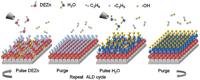
When doping ZnO, a popular and easy to implement method is to add an additional cycle with the dopant precursor after a set number of ZnO cycles. This is called delta doping and the dopant concentration can be varied by changing the ratio of ZnO cycles to dopant cycles. Sometimes this can result in suboptimal film properties due to uneven dopant distribution. Studies have combatted this by increasing dopant dispersion through the use of precursors with increased steric hinderanc, 32 the release of a chemical before or after the dopant precursor,33,34 and adjustment of process timings.35,36 An alternative method of doping is co-doping, where the substrate is exposed to a mixture of the dopant precursor with the relevant ZnO precursor (either the Zn or O source).6,37,38 Note that the ratio of dopant to Zn or O precursor used in depositions does not necessarily lead to films of that composition due to differences in reactivities, 37 exchange reactions 39 etc.
ALD deposition variables
A number of deposition variables in ALD need to be optimised and controlled in order to ensure true, self-saturating ALD occurs and to influence the deposited material's properties.
ALD processes tend to have a temperature range in which the growth per cycle (GPC) is fairly constant; this is known as the ‘ALD window’ and it differs with precursor selection. 1 The ALD window for the DEZ/H2O process is generally reported as being between around 110 and 170°C, 17 with a GPC of around 0.2 nm/cycle within this range, and decreasing GPC with increasing departure from the ALD temperature window. Nevertheless, ZnO is frequently grown outside the ALD window temperature range, with extremes from room temperature40,41 to 400°C, 42 as self-saturating ALD growth still occurs and the different properties in these ranges can be desirable, as described later. This wide and low deposition temperature range is one of the advantages of the DEZ/H2O combination of precursors.
Precursor exposure time and the purge time between releases need to be controlled. Methods will depend on the ALD equipment used. There are several different types of ALD reactor; 5 one type is the conventional ALD reactor where substrates sit on a stage in a vacuum chamber and precursors are released into the chamber sequentially, with a purge time between each precursor exposure. There is flexibility to independently adjust exposure and purge times with this arrangement.
A different type of reactor is the Spatial ALD (SALD) reactor, where precursor exposure is separated in space rather than time.
7
Many SALD reactors do not require a vacuum chamber; they are often used in open atmosphere and then are generally known as atmospheric pressure SALD (AP-SALD) reactors.
6
A common form of AP-SALD involves a coating head containing a series of channels, each constantly releasing and removing precursor or inert gas, passing over the substrate surface. The exposure and purge times are therefore defined by the speed with which the substrate surface passes under the deposition head which means limited flexibility on individual control but allows growth rates of nanometres per second.29,43 Figure 2 shows a schematic example of both of these reactors and the timings of the precursor exposure and purging of the substrate.
a The conventional ALD and spatial ALD reactors and b the exposure of the substrate to precursors (I) and (II), and inert gas. The spatial ALD exposure is considered at point Q on the substrate. Reproduced with permission from Ref.
44
Copyright 2009 IEEE.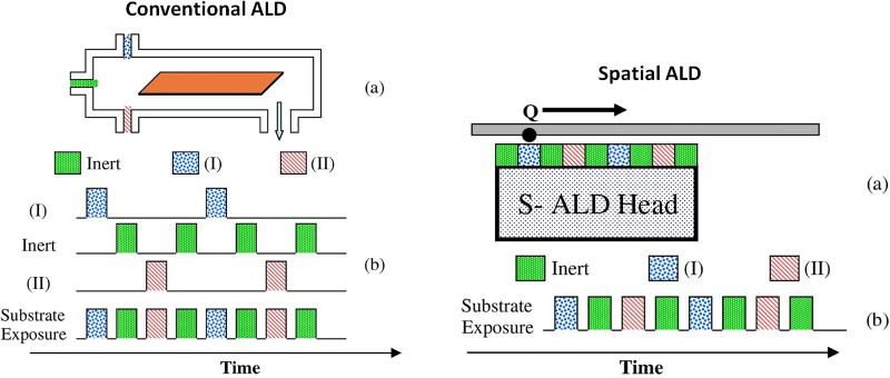
Comparison with other techniques
The uniformity and conformality of ALD coatings was mentioned previously, arising from the self-saturating surface reactions. Common alternative thin film deposition methods include physical vapour deposition processes such as molecular beam epitaxy, pulsed laser deposition, and sputter deposition, and chemical routes, for example spray pyrolysis, sol-gel and chemical vapour deposition (CVD). In comparison, ALD is much more uniform and can be used for very complex, high aspect ratio surfaces, not just for line-of-sight deposition as with the physical deposition methods, and produces very repeatable films. 45 The main drawbacks are relatively slow deposition speed and the cost of equipment.
The ALD process is comparable to CVD. With CVD higher temperatures are used, and the gaseous precursors are released simultaneously over the substrate, leading to much higher deposition rates but reduced conformality. CVD can be carried out with precursors used in ALD; indeed, if purging is not sufficient between ALD precursor exposures then there can be a CVD contribution to the growth. 1 AP-SALD reactors can sometimes be operated in a CVD mode, resulting in higher deposition rates but reduced uniformity. 6
ZnO in devices
ZnO is a widely used material in devices for many reasons, including its element abundancy, wide bandgap and high transparency to visible light. 46 Its non-toxicity and higher transparency are advantageous compared to commonly used CdS for Cu(InGa)Se2 (CIGS)-based solar cells. 47 Various other metal oxides alternatives exist to ZnO in devices; TiO2 has a similar band structure and can also be grown easily by ALD, so is often used for the same applications. 22 The high mobility of ZnO is one of its advantages compared to TiO2, but sometimes TiO2 has better charge transfer characteristics. 48 The surface of ZnO is particularly complicated, partially due to polarity from its wurtzite crystal structure, and the properties of ZnO are highly dependent on deposition technique. 49
ZnO produced by ALD tends to be crystalline even at very low temperatures. ALD ZnO is generally n-type with a relatively high carrier concentration on the order of 1018–1019 cm−3 unless deposition adjustments are made to reduce the electron concentration. The high electron concentration is linked to oxygen deficiency in the films,50,51 but the specific origin is unclear. 46 The reduction of electron carrier concentration to improve device performance is one of the key points of discussion in this review.
Different devices will be considered in this review, examples are shown in Fig. 3. Note that in some cases a conductive ZnO layer e.g. B-doped ZnO, Al-doped ZnO, is employed in combination with the discussed ZnO, but as stated earlier, this application is outside the scope of this review.
Examples of device types discussed in this review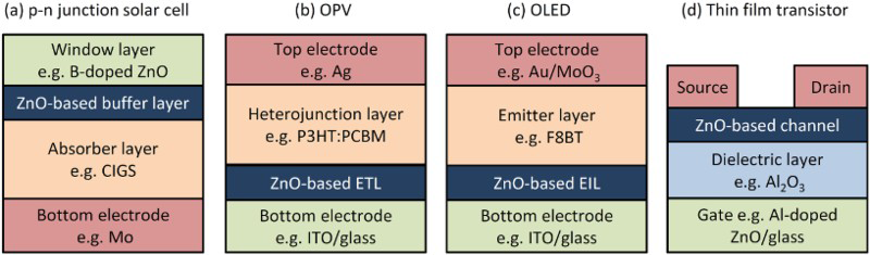
One of the first applications of ALD ZnO was as an n-type layer for inorganic solar cell heterojunctions, namely in CIGS-based solar cells.52–60 CIGS is the p-type light absorbing layer in these solar cells, and forms a p-n heterojunction with the buffer layer material, which separates the free carriers created on light absorption. 61 ALD ZnO has been employed as the n-type buffer layer in these cells (Fig. 3a) and in analogous situations, such as in combination with Cu2O28,62,63 and in Pb-based quantum dots cells.64–67
Organic photovoltaics (OPVs) have potential as inexpensive, printable, flexible devices, although challenges still exist with obtaining and maintaining stability and efficiency. OPVs function by having a heterojunction of an absorbing organic material, which acts as a donor (e.g. poly(3-hexylthiophene-2,5-diyl) (P3HT)), in contact with an organic electron acceptor (e.g. phenyl-C61-butyric acid methyl ester (PCBM)). The excited state that forms on light absorption (exciton) dissociates at the donor–acceptor interface and the free charge carriers are transported through the organic network to the electrodes. 68 For these cells it can be necessary to insert an electron transport layer (ETL) (otherwise known as a hole blocking layer) to ensure selectivity i.e. reduce carrier recombination at the cathode. ZnO is frequently employed for this purpose, including ZnO deposited by ALD (Fig. 3b).69–77 Similarly, ALD ZnO can also be incorporated in hybrid solar cells, where the exciton dissociates at an organic/inorganic interface such as P3HT/ZnO.78–80
Another developing optoelectronic device that relies on semiconducting organic materials is the Hybrid Light Emitting Diode (HyLED). 81 Typically HyLEDs consist of an organic emitter layer sandwiched between two electrodes, and light is released on electron–hole recombination within the emitter e.g. poly[(9,9-dioctylfluorenyl-2,7-diyl)-co-(1,4-benzo-{2,10,3}-thiadiazole)] (F8BT). ALD ZnO has been used as an electron injection layer (EIL) (also sometimes hole blocking layer) in this type of device on the cathode side (Fig. 3c). 82 More recently the emerging perovskite based materials have also been investigated as emitters for LEDs 83 and absorbers for PVs84,85 with ALD ZnO being incorporated into such devices for similar purposes.
TFTs with ALD ZnO channel layers have also been fabricated (Fig. 3d).27,86–103 Key operating parameters, including turn-on voltage, carrier mobility, on/off current ratio and stability are important for optimisation, 104 and transparency can be necessary for lighting applications which has led to transparent TFTs being produced entirely by ALD and print patterning. 105 These and other devices, such as diodes,106,107 photoelectrodes108–110 and inorganic LEDs,23,111 will be included in the discussion.
ZnO deposition variables
The properties of ALD ZnO can be tuned during deposition or modified post-deposition, for example by plasma treatment112,113 or annealing under a specific atmosphere.114–118 The focus here is on tuning through ALD deposition variables as this is an effective method with much scope 119 and avoids an additional fabrication step which may also be incompatible with the device design e.g. for flexible substrates. The important results for each variable are presented individually, but note that a change in one parameter may mean an adjustment is needed in another, for example longer purging times are necessary at low temperatures. If not otherwise specified, the layer involved is intrinsic ZnO deposited using DEZ/H2O.
Deposition temperature
ALD ZnO has a huge variation in properties with deposition temperature, explored in detailed investigations on solo ZnO layers.41,51,120,121 Both the carrier concentration and mobility of ZnO decrease at low temperatures (Fig. 4). Change crystallinity is likely partially responsible for this behaviour, and the carrier concentration is greatly affected by the ZnO becoming increasingly less oxygen deficient.50,51
The deposition temperature dependence of the carrier concentration, mobility and resistivity of intrinsic ZnO films. Reproduced with permission from Ref.
25
Copyright 2012 IOP Publishing.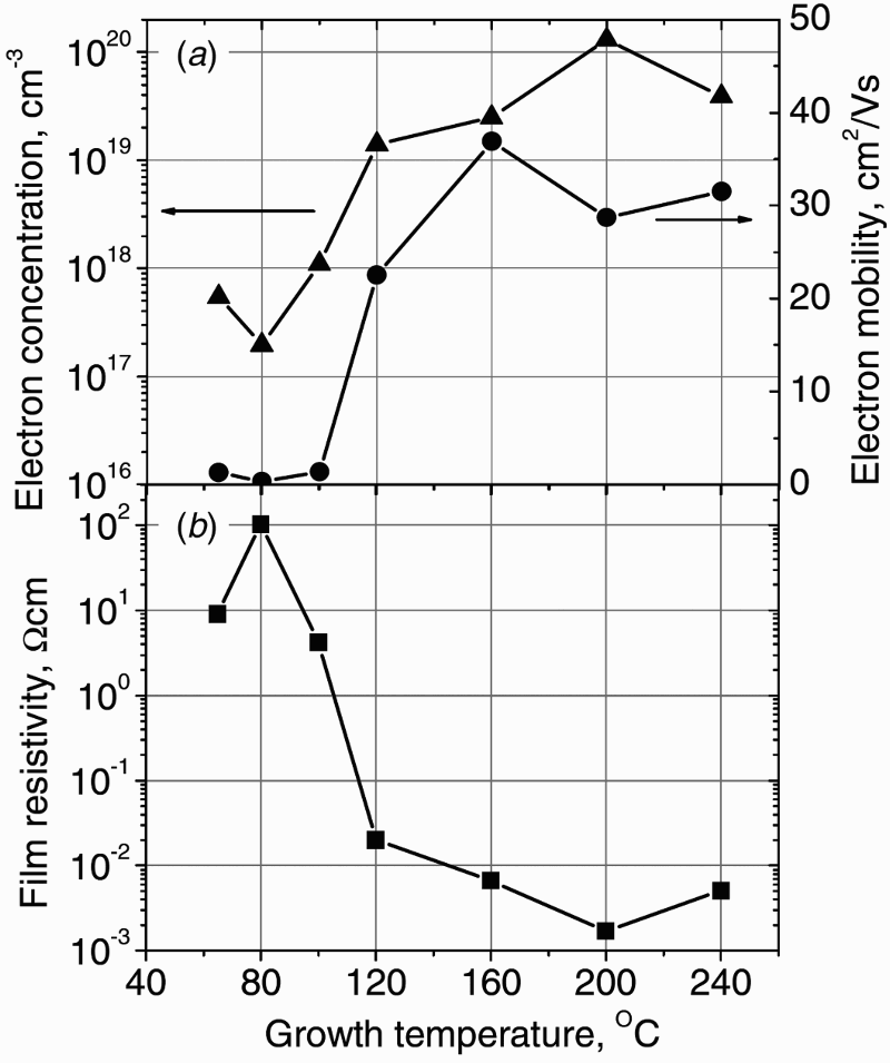
In CIGS-type solar cells, an early report showed that the lowest temperatures used, 120°C, gave the most stable and reproducible solar cells. 54 Later publications moved more towards doped ZnO layers, and a study of (Mg,Zn)O layers in CIGSe found that high deposition temperatures of 150–180°C also resulted in a large drop in efficiency.55,56,60 This temperature dependence was initially tentatively suggested to be due to difference in (Mg,Zn)O nucleation at higher temperatures56,60 but, after further study, it was concluded that the higher conductivity of the (Mg,Zn)O buffer layer in the area immediately adjacent to the CIGSe interface was the governing cause. 55
Where ALD ZnO has been used as an ETL, low temperatures have often been chosen due to flexible substrate compatibility aims and to ensure sensitive organic semiconductors are not damaged. Advantageously, devices have frequently shown improved properties with low temperature ALD ZnO, attributed to the enhanced hole blocking of the ZnO. 69 However, very low temperatures can be detrimental; ZnO layers produced at 45°C hindered the OPV compared to those at 80°C due to the reduction in surface hydrophobicity and therefore active layer adhesion. 70 In HyLED devices, particularly if holes accumulate near the EIL, the increased hole blocking of lower temperature ALD ZnO also improves performance. 82 The lower temperature is also beneficial in TFTs as they can fail to be switched off within reasonable gate voltages if the channel carrier concentration is too high to be depleted.89,96–98
In addition to the above examples of controlling the deposition temperature for ZnO property optimisation, the deposition temperature can also be used to optimise the substrate properties. A key example of this is in Cu2O/(Sn,Zn)O solar cells when DEZ/H2O2 are used as the Zn/O precursors.
62
Interest in this solar cell structure has arisen because of the non-toxic, earth abundant elements involved; however, there can be trouble forming a good heterojunction due to the very rapid formation of CuO at the surface of Cu2O on air exposure.
122
Careful selection of the ALD deposition conditions has been used to reduce CuO on the surface of Cu2O. Exposure to DEZ reduced the Cu(II)O to Cu(I)2O, and the oxidation of Cu(I)2O to Cu(II)O by H2O2 was found to be temperature dependent (Fig. 5). Lower deposition temperatures therefore reduced CuO, with 70°C producing the highest efficiency cells (2.85%). Deposition temperature control approaches to reducing CuO have also been reported elsewhere.
122
X-ray photoelectron spectroscopy demonstrating the sensitivity of Cu2O to H2O2 pulses at different temperatures. Reproduced with permission from Ref.
62
Copyright 2014 Wiley-VCH Verlag GmbH & Co. KGaA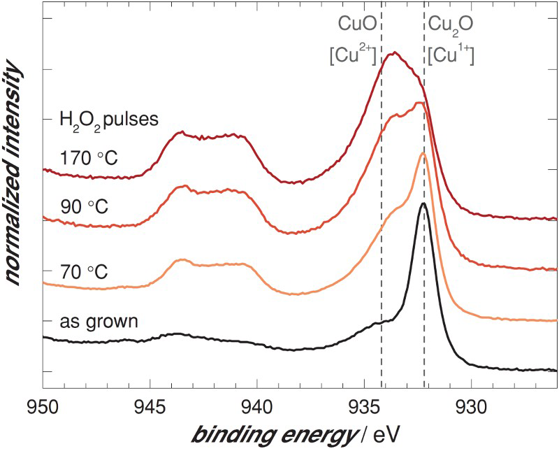
However, low deposition temperatures are not necessarily always optimal. A study of n-ZnO/p-Si solar cells found the highest deposition temperature used (160°C) showed the best efficiency. 123 The likely reason for this is that the performance-determining factor was the relative carrier concentrations of the p-Si and n-ZnO, making the depletion width within Si very small when using lower temperature ZnO. Nevertheless, the diode ideality was improved with lower temperature layers, as reported in other n-ZnO/p-Si studies. 124 Additionally, there are examples where there is no temperature study but high ZnO deposition temperatures have produced good performances. Ultrathin (<5 nm) films67,71 and OPVs with a P3HT:PCBM heterojunction 72–74 appear to be common examples.
It is clear that device-specific performance limiting factors sometimes do not favour the low carrier concentrations but the examples above along with additional cases where low temperature ZnO has been employed efficaciously without a systematic temperature study76,79,85,125,126 demonstrate that low deposition temperatures and the resulting low carrier concentrations are often advantageous. The control of deposition temperature is frequently the most effective way of optimising intrinsic ZnO layers in devices.
Purge and exposure times
In ALD, the selection of precursor exposure time is usually a balance between ensuring self-saturation has occurred for uniform coverage of a surface, 30 and minimising the wastage of unreacted precursor. For purge times, the shortest length which still allows precursor removal thus avoiding gas phase reactions is often selected, and purging is usually the longest step in a deposition cycle. The low growth rates are one of the drawbacks of using conventional ALD but this can be outweighed, especially for thin films, by the benefits such as low temperature capabilities and sub-nanometre thickness control and uniformity.
The high reactivity and vapour pressure of the DEZ/H2O precursor combination allows relatively short exposure for general ZnO growth, but the exact timings are reactor and temperature dependent. Longer precursor exposure times (sometimes by using a flow-interrupting hold step) and lengthy purging can be necessary to allow diffusion through very high aspect ratio substrates. 127 The ability to uniformly coat complex 3D surfaces is unique to ALD and has, for example, allowed the infilling of temperature sensitive quantum dot thin films. PbSe quantum dot films had mobility enhanced by up to an order of magnitude through ALD Al2O3/ZnO coating which lowered the inter-crystal electron tunnelling barrier. 66 Infilling has also used in applications of LEDs and solar cells.128–130
Not only do exposure and purge times have to be tuned for uniformity and efficiency purposes, but they can also affect material properties. In conventional ALD, fine tuning of ZnO properties is possible through H2O purge times, with the effects linked to –OH groups.36,69 Reports of deposition at intermediate temperatures find the GPC decreases and resistivity rises with increasing purge times, 131 but at a lower temperature (90°C) longer H2O purging results in higher mobility ZnO, improving OPV efficiency. 69 Thus some improvements are possible but at the expense of growth rate.
Purge times are limited to being relatively long in conventional ALD whereas millisecond purge times are possible in AP-SALD, producing more dramatic effects on ZnO properties. Decoupling the different purge and exposure times in AP-SALD revealed ultrafast purge times change the GPC (related to both H2O and DEZ purge) and lower carrier concentration significantly (due to DEZ purge time reduction). 27 In TFT studies, turn-on voltages were shifted considerably towards 0 V with shorter DEZ purge times while the mobility was also improved. AP-SALD ZnO has been effective at hole blocking 75 and the ultrafast purge times are likely to be good for buffer layers. 29
Exposure times in ALD can also be used to control properties132,133 and extended precursor exposure times can improve crystal quality of epitaxial films 134 and increase bias stability in TFTs. 135 However, of all these exposure and purge affects, ultra-short DEZ purge times have the most significant effect on ZnO electrical properties.
Film thickness (number of cycles)
The optimal thickness of ALD ZnO varies across device types due to disparate layer requirements, but it is often similar to that of ZnO deposited by other techniques for the same application. Commonly used are thicknesses in the range of 10–150 nm. Note that partially due to the often non-uniform grain structure the properties of films of these thicknesses are not necessarily representative of bulk ALD ZnO.
136
Growth initiating from many ZnO nucleation sites on a substrate surface leads to numerous grain boundaries near that interface. The grain boundary concentration decreases through the film thickness as growth of the more favourable grains dominates, resulting in a large in-plane grain size at the surface (Fig. 6). Whether a critical interface is on top or below ZnO can therefore have a huge effect as grain boundaries can contain carrier scattering and recombination centres.
137
Increased surface area for charge transfer
138
due to the higher roughness may be beneficial.
The evolution of the grain structure of ZnO on Si with an increasing number of ALD cycles. The data point Z1-5 in graph f correspond to the top and cross-sectional views of samples a–e, respectively. Reproduced with permission from Ref.
139
Copyright 2013 Elsevier.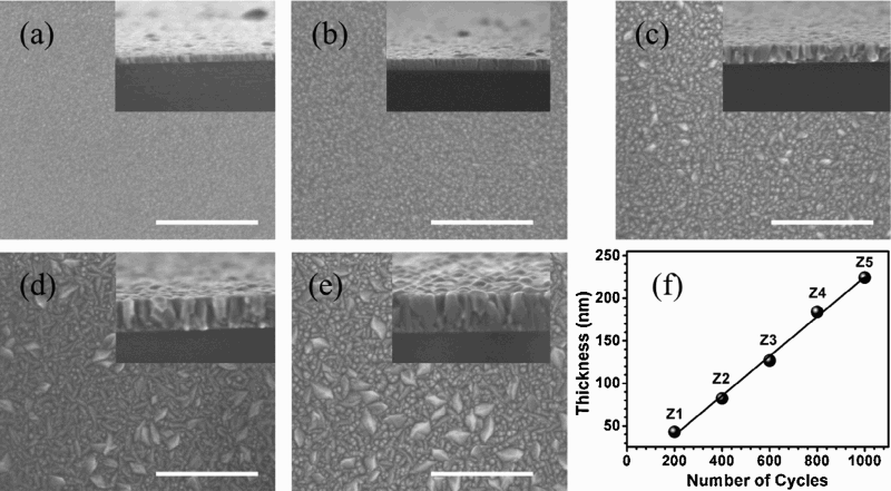
In general, transistors show better switching performance with thinner films due to the necessity of depleting the channel. 117 Frequently in solar cell, OPV etc. applications the thickness dependence follows one of two trends: either a minimum thickness is required and then performance is thickness-independent or an intermediate thickness is optimal. A minimum thickness has been reported for a P3HT:PCBM/ZnO/ITO OPV structure; ZnO layers <10 nm resulted in unfavourable s-shaped current–voltage curves. 72 The work function of the ZnO/ITO electrode did not vary with thickness, and the current–voltage curve shape for the thinner layers was improved by ultraviolet (UV) illumination, attributed to desorption of oxygen molecules at grain boundaries. Similar desorption under UV has been seen, for example, using He plasma 113 and with Zn(O,N) based transistors where water adsorption then recovered their original behaviour. 103 Another study using the same OPV structure reported a larger critical thickness (40 nm). If the critical thickness is dependent on grain boundaries, 72 then the difference in deposition conditions and hence difference in crystal structure could explain these contrasting results. Other reports of a minimum layer thickness include (Zn,Mg)O with CIGS 56 and thicker layers can sometimes give better long-term device stability. 58
Where optimum intermediate thicknesses of ZnO have been reported the frequent explanation is a balance between the increased shunt resistance (CIGSs cell), 57 hole blocking (OPV) 70 or exciton dissociation (perovskite) 85 and the added series resistance of thicker layers. Optical interference effects 140 and electrode Schottky barriers 141 also depend on ZnO thickness and will influence the performance of some optoelectronic devices. The behaviour of ZnO growing on organic layers is very different, as infiltration of the precursors into the organic is often seen.142,143 This effect has been used to the map the morphology organic active layers 144 and hybrid solar cells can be formed.79,80
In ultrathin ZnO films, quantum confinement in the small grains has been reported due to Bohr radius lengthscales.145,146 The growth mechanism of ALD also leads to some unique properties of ultrathin films not applicable to other deposition techniques. The creation of completely continuous ZnO layer requires at least several ALD cycles,147,148 can need 10 s of cycles117,137,149,150 and is very substrate dependent. 151 Growth can initiate as amorphous71,147 or crystalline 148 depending on conditions, but thicker films tend to be crystalline. In one case of using ultrathin ALD ZnO layers in an OPV 2 nm layers were optimal, where the island growth had not coalesced, avoiding the creation of unfavourable grain boundaries. 125 For another ultrathin ETL, highest performance occurred with 3.4 nm ZnO, just after the amorphous to crystalline transition. 71 Using ultrathin ZnO based layers has been reported as beneficial in other cases of passivation and recombination reduction,28,67,76 for chemical reduction of the substrate,62,152 and just using even a single cycle of ZnO can improve the photocurrent of Cu2O-based photocathodes. 110
Precursors and doping
Alternative precursors
In the majority of ALD cases, ZnO is deposited using DEZ and H2O as precursors. Advantages include the high reactivity and high room temperature vapour pressure of the precursors; the inexpensive, commonly used and safe H2O precursor; the wide and low temperature ALD window; the well-researched range of properties possible and the purity of the deposited ZnO. There are alternative combinations of precursors which can also be used to grow ALD ZnO, such as Zn acetate, dimethyl zinc (DMZ), and ZnCl2 as zinc sources, and O2 plasma, O3, N2O, H2O plasma, H2O2 and O2 as oxygen sources. 17 Note that the precursors and ALD windows have to be compatible with any dopant precursors used too.
In the devices types considered here, not all the possible precursor combinations have been used. Of the zinc containing precursors, DEZ is easily the most popular choice. The higher deposition temperatures of some of the other options (e.g. ZnCl2) may have dissuaded their use. DMZ has a higher GPC than DEZ with H2O, attributed to less steric hindrance (but similar GPC with H2S for ZnS due to H2S corrosion), 153 but the mobility and carrier concentration are lowered due to residual impurities. 154 DMZ/H2O has been used for device fabrication, with similar results to DEZ/H2O. 25
Alternative oxygen sources have been more frequently used as precursors for ZnO layers in devices, especially in transistors e.g. N2O, 101 O2. 102 Precursors such as O2 plasmas can be used at a range of temperatures including low temperatures, and the higher reactivity produces more stoichiometric films resulting in a lower carrier concentration than the DEZ/H2O combination. 155 Plasmas can also aid initiation of ZnO growth on polymer surfaces, 156 which has been used in a study of ZnO growth on and in a hybrid solar cell active layer. 79 Studies on plasma ALD ZnO channel layers produced high stability, high mobility TFTs,99,100 with improved gating compared to DEZ/H2O due to higher resistivity. 157 DEZ/O2 plasma has also been used in OPVs but performance was not improved due to the defects created. 77
Choice of precursor is not always made for reasons of ZnO property optimisation, other motivations such as the avoidance of underlayer degradation can be important. For example, methylammonium lead trihalide (CH3NH3PbX3) perovskites, a popular area of research, present processing challenges due to their sensitivity to elevated temperatures, hydration on water exposure that can lead to degradation, 158 and problems with self-saturating ALD reactions e.g. with Al2O3 deposition. 159 AP-SALD has the advantage of high deposition rates, significantly reducing time at elevated temperatures, and has been used to deposit ZnO and (Zn,Mg)O directly onto perovskite for use as an LED. 83 The choice of oxygen source was crucial, with a switch from H2O to O2 precursor resulting in LED turn-on percentage improving from 15 to 60%. In inverted solar cells, the DEZ/H2O combination has been used to deposit ZnO on PCBM coated perovskite, where the perovskite layer was only exposed in areas of incomplete PCBM coverage. 84 It is clear that alternative ZnO precursors have a key place in device applications and there is scope for more investigation in this area.
Doped ZnO
Doping is a highly effective method of controlling many ZnO layer properties. Sometimes device limiting factors, for example band alignments, cannot be overcome with intrinsic ZnO, so doping has proved a crucial next step to performance improvements. The main types of doping are here described, however there are other doping combinations that have been reported e.g. a-InGaZnO for transistors. 160 Note that the properties of the film produced depend highly on the ALD precursor combinations and deposition conditions.
Band alignment engineering
One of the properties that has held ZnO back in solar cell and LED applications is the ZnO conduction band (CB) offset, which is often found to be quite negative for commonly used absorbers/emitters. In CIGS solar cells a slightly positive buffer layer CB offset is found to be optimal; negative CB offsets lead to high charge recombination. Increasing Ga content in CIGS shifts its CB positive, so while 0% Ga (CIS) cells operate well with undoped ZnO,53,54 doping of ZnO with S has been implemented to improve the operation of Ga containing cells by inserting a DEZ-H2S cycle after a set interval of DEZ-H2O cycles. Reducing the DEZ-H2S interval caused the CB offset to shift to positive, reducing interface recombination, but the larger CB offset at high S compositions also started to act as barrier to current flow59,161 (Fig. 7). Note that sulphur content is found to vary through Zn(O,S) film thickness. The ZnS crystal structure can be cubic or wurtzite (with different lattice parameters from ZnO), and intermediate Zn(O,S) compositions can produce an amorphous phase.153,162,163 Carrier concentration and mobility reduce with S doping.
Schematic band diagram showing the alignment of the Zn(O,S) conduction band minimum (CBM) and valence band maximum (VBM) relative to CIGS. Reproduced with permission from Ref.
59
Copyright 2006 American Institute of Physics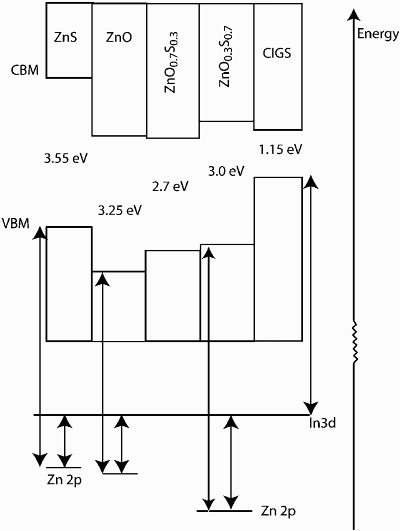
The band gap engineering approach can also be taken with ZnO dopants other than sulphur. Magnesium doping and tin doping of ZnO can also improve the CB offset in devices. 21 In one comparative investigation, the band alignment of Zn(O,S) with Cu2O absorber cells was seen to be more favourable than that of (Zn,Mg)O, ZnS or ZnO. 63 The decision on whether to use Zn(O,S) (Zn,Mg)O or (Zn,Sn)O in a device might, however, rest on additional factors, e.g. the risk of using H2S as a precursor. 164
The wide bandgap of MgO made the (Zn,Mg)O initially attractive for band gap engineering purposes, as the CB level is raised through hybridisation of Mg 3s orbitals with the Zn 4s orbitals. 165 Excellent improvements in device performances have been reported with ALD (Zn,Mg)O layers in CIGS cells, 56 in quantum dot solar cells, 64 in hyLEDs 166 and in perovskite LEDs. 83 (Zn,Mg)O has a dopant level dependant crystal structure, with transitions from wurtzite to rocksalt structure 60 with increasing Mg content, along with decreasing carrier concentration and mobility as the electrical properties transform from semiconducting ZnO to insulating MgO. In a comparison with Zn(O,N), the improvements from (Zn,Mg)O were confirmed to be predominantly due to the CB offset control rather than the carrier concentration reduction. 64
Along with CB offset engineering, Sn doping of ZnO can produce amorphous layers, although films can contain crystallites within the amorphous layer for some depositions. 167 ALD (Sn,Zn)O can produce good performance in TFTs together with stability against crystallisation. 26 ,168 The amorphous (Sn,Zn)O layers have also produced efficiencies rivalling reference CdS layers in CIGS solar cells 169 and acted as effective, ultrathin buffer layers in Cu2O solar cells.28,62 The increasing disorder around the Zn atoms with increasing Sn composition has been seen to decrease the mobility of amorphous (Sn,Zn)O films. 170
Carrier concentration control
Nitrogen doping of ZnO by ALD can be used for the purpose of electron concentration reduction. Nitrogen is used to substitute in the place of oxygen in ZnO and act as an acceptor 171 but the nature of the N dopant in ALD films is likely to be more complicated. For example, N–H has been found to be present when an NH3 precursor (in the form of NH4OH) is used. 87 The amount of nitrogen incorporated in ALD Zn(O,N) films tends to be much smaller than the ratio of NH3/H2O precursors, attributed to exchange reactions, 39 and carrier concentration is around 1016 cm−3. 172
The nitrogen doping has been shown to be effective PbS quantum dot solar cells, producing a higher open circuit voltage than undoped ZnO because the lower carrier concentration reduced recombination. PbSe quantum dot solar cells were not affected by the nitrogen doping, revealing that the performance improvement is dependent on whether recombination is dominant in the absorber layer or at the interface. 65 The lower carrier concentration improved rectification in photodiodes, 107 increased ZnO UV emission in LEDs, 111 improved TFT switching over ZnO 87 and dependence of performance on atmosphere is removed. 173
Multilayers
Multilayers can be employed in devices in order to elucidate performance critical factors, such as in CIGS cells where only the carrier concentration of the (Zn,Mg)O at or near to the CIGS/buffer layer interface was found to be important. 55 In another study, combining the properties of two differently doped (Zn,Mg)O layers in a bilayer reduced interface recombination. 174 Multilayers can also be used to modify the properties of subsequently deposited ALD layers. An underlayer of Al doped ZnO improved uniformity of ALD TiO2 in photocathodes by producing a more hydroxylated surface.108,109 In another example, the deposition of a first layer of ZnO at high temperature (300°C) was used to control the orientation of a following, thicker layer of ZnO at a lower temperature (150°C). 23 The high temperature of the first layer enabled (002) oriented growth, but the GPC at these temperatures is around half of that at lower temperatures, so using a lower temperature for the second layer maintained the (002) orientation while reducing the deposition time. Stimulated emission was observed in these double layers but not for lone low temperature ZnO layers which had mixed orientations. Conversely, thin Al2O3 layers can be used block surface polarity of ZnO nanowires to control ALD ZnO orientation for nanostructures. 175
In bottom gate transistors, the crystallinity of a ZnO channel layer has been shown to depend on the dielectric on which it is grown,86,88 and multilayers have been employed to reduce the ZnO interface defects. 105 The use of a 5 nm high temperature ZnO layer underneath 35 nm of 100°C ZnO layers increased the field effect mobility without sacrificing turn-on voltage. 89 Interfacial layers of Al doped ZnO have likewise had beneficial effects,90–92 as has sandwiching the ZnO channel between (Zn,Hf)O layers, which also increased the stability by suppressing the adsorption of oxygen at grain boundaries. 93
There are reports of reasonable and improved stability with devices incorporating ALD ZnO layers. 176 However, ZnO can suffer degradation in the long term. ALD ZnO layers exposed to damp-heat have been seen to undergo a several orders of magnitude reduction in mobility along with a slight reduction in carrier concentration, attributed to diffusion of gases along grain boundaries and the creation of crystal defects which act as traps and recombination centres. 177 Therefore, to prevent degradation of properties with time it can be advantageous to coat ZnO with a protective layer if one is not already incorporated in device design. ALD is a good technique for passivation and encapsulation layers due to the high quality, pin-hole free coating, 19 and is an easy step to add for devices which already have ALD ZnO layers, but choice of the passivation layer can affect the ZnO underneath. For example Al2O3 is a common layer in TFTs but has been seen to affect the performance 94 e.g. by increasing carrier concentration (attributed to the trimethyl aluminium). 95
Conclusions
This review has highlighted a variety of ways to improve n-type semiconducting ALD ZnO layers. With the described combination of methods, a wide variety of ZnO properties can be achieved. Two key approaches to improve solar cell, TFT and LED devices have been to reduce ZnO carrier concentration or to use CB offset engineering. Frequent methods of carrier concentration reduction include using low deposition temperatures, nitrogen doping and alternative precursors as oxygen sources, but ultra-short DEZ purge times in SALD have more recently appeared as a potentially leading method for future industry. Doping of films with sulphur, magnesium and tin has enabled tailoring of CB offsets in solar cells and LEDs, improving the performance considerably and looks to be a promising area for research. The high control over these ZnO based layers and the use of multilayers has enabled detailed investigation into the functioning of devices, identifying performance limiting factors and finding new routes for improvements.
Footnotes
Acknowledgements
The author would like to acknowledge Dr Martyn McLachlan for support and advice. This work was supported by the Engineering and Physical Sciences Research Council through the Imperial College Doctoral Training Award scheme.