
Abstract
Gallium nitride (GaN)-based light-emitting diodes (LEDs) are highly energy efficient and their widespread usage in lighting can induce significant worldwide electricity savings. To achieve white and colour-tuneable lighting, the mixing of light from red-, blue- and green-wavelength LEDs is desired. At present, the efficiency of green-wavelength LEDs is only about half of that of red- and blue-wavelength LEDs, which is also known as the ‘green gap’ problem. Cubic zincblende GaN has the potential to bridge the ‘green gap’ due to the theoretical absence of internal electric fields that plague the commonly used c-plane hexagonal wurtzite structure. This review first looks at the various methods of achieving metastable zincblende GaN, and examines the crystal defects present. Then the different components towards a full zincblende GaN LED structure, including p- and n-type doping, zincblende InGaN and AlGaN on GaN heterostructures, together with the problems that need to be overcome to achieve green-wavelength emissions are reviewed.
This review was submitted as part of the 2017 Materials Literature Review Prize of the Institute of Materials, Minerals and Mining run by the Editorial Board of MST. Sponsorship of the prize by TWI Ltd is gratefully acknowledged
Introduction
In the UK and around the world, about 20% of electricity consumption is typically used on lighting [1]. Therefore, a significant amount of electricity can be saved using highly energy-efficient light-emitting diodes (LEDs) as light sources instead of the traditional incandescent and fluorescent lighting. At present, virtually all commercial LEDs that emit white light consist of a blue-wavelength gallium nitride-based (GaN) LED capped with a phosphor. The phosphor absorbs parts of the blue spectrum and re-emits the other colours in the visible spectrum of longer wavelengths, with the superposition of the different wavelengths producing white light. Since there is inevitable energy loss during the wavelength conversion in the phosphor, a more energy-efficient system of producing white light is to mix light from red, blue and green LEDs, with the additional benefit that their intensities can be varied to produce colour-tuneable lighting. The ability to tune the wavelengths of indoor lighting throughout the day has potential health benefits, as studies have suggested that exposure to bluewavelengths in the evenings through LED-lit devices suppresses the body's production of melatonin, a hormone that promotes sleepiness [2].
LED structure and operation
A schematic of the structure of an LED is shown in Figure 1. Applying a forward-bias across the p- and n-contacts results in holes generated in the p-type layer and electrons generated in the n-type layer moving towards the InGaN/GaN multiple quantum wells (MQWs) region. Since the GaN/InGaN heterostructure is Type I as shown in Figure 3(c), the carriers are spatially confined within the InGaN quantum wells where radiative recombination occurs between electrons and holes to produce photons. It is also possible that non-radiative recombination takes place instead, for example due to impurity states within the band gap to produce phonons. The efficiency of an LED is often expressed in terms of the internal quantum efficiency (IQE) and external quantum efficiency (EQE), which are the ratio of radiative electron-hole recombinations to number of injected carriers, and the ratio of emitted photons to injected carriers, respectively.
Schematic of an LED structure with InGaN/GaN MQWs as active layers and light extraction via a cleaved side facet.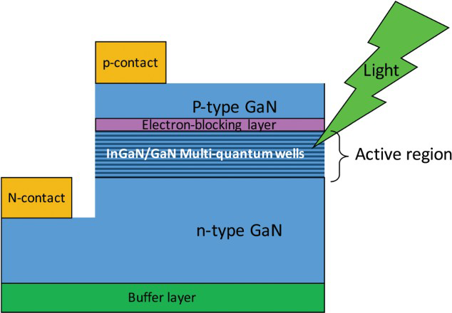
The emission wavelength of the InGaN quantum wells can be tuned by the indium content (by changing the band gap energy, as shown in Figure 2) and the thickness of the quantum wells. Higher indium contents and thicker quantum wells are required to achieve green emission wavelengths. From Figure 2, which presents Γ-valley energy gap values for relaxed III-nitride layers at 300 K, the indium contents of InxGa1−xN alloys that have green emission band gaps of 2.3 eV are x = 0.26 and 0.31 for the zincblende and wurtzite structures, respectively. Since the InGaN quantum wells are strained in LEDs, the band gap is calculated to be 0.173 eV larger for fully strained InxGa1−xN (x = 0.26) layers compared with relaxed layers, using the method in Morkoc et al. [5] and material constants from Vurgaftman et al. [3].
Γ-valley energy gaps at 300 K of wurtzite and zincblende III-nitrides. Energy gaps are plotted as a function of lattice parameter awz for wurtzite and azb/√2 for zincblende, both of which correspond to the distance between group-III ions in the (001) plane. Values from Vurgaftman et al. [3] and As et al. [4].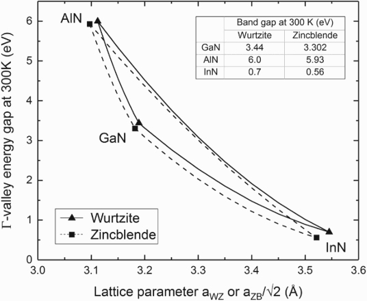
The ‘green gap’ problem
Currently, green indium gallium nitride (InGaN) LEDs have only less than half the EQE of blue InGaN and red aluminium gallium indium phosphide (AlGaInP) LEDs [6], and this is known as the ‘green gap’ problem. Phosphide-based LEDs for green-wavelength emission suffer from an indirect bandgap which lowers the radiative recombination efficiency. For nitride-based LEDs, the band gap is direct, but there are several possible factors that can contribute to the ‘green gap’ problem, with all of them related to the requirement that a higher indium content of around 11% is required in the InGaN quantum wells for emission of green wavelengths (540 nm) compared to blue wavelengths (470 nm) for the wurtzite crystal structure.
Most of the commercial LEDs are currently grown in the c-plane (0001)-oriented hexagonal wurtzite crystal structure, which results in piezoelectric and spontaneous polarisation fields in the [0001] growth direction across the LED device structure. Electric fields across the LED structure result in the quantum confined Stark effect (QCSE), which is the spatial separation of electron and hole wavefunctions within a quantum well, as shown in Figure 3(d). (A more detailed discussion of the QCSE and its effects is given by Ren [8]). Although all working diodes are subjected to the QCSE due to external bias, the internal piezoelectric and spontaneous electric fields present in the c-plane wurtzite crystal structure exacerbate the effect. With a smaller spatial overlap between the electron and hole wavefunctions, there is a lower rate of radiative recombination. In order to reduce such internal electric fields, many groups have focussed their studies on wurtzite with non-polar (m-plane and a-plane) and semi-polar orientations, but the efficiencies such LEDs have not been as high as expected and fall behind those of c-plane wurtzite LEDs [8]. Throughout this review, the c-plane orientation is implied where the wurtzite structure is mentioned, unless explicitly stated otherwise.
(a) and (b) Crystal structures of cubic zincblende and hexagonal wurtzite III-nitrides, respectively. Reprinted from Hanada [7], with the permission of Springer. Band diagrams of an InGaN quantum well with GaN barriers without external bias: (c) in the absence of internal electric fields for the (001)-oriented zincblende structure, (d) in the presence of internal electric fields for the c-plane (0001)-oriented hexagonal wurtzite structure resulting in bending of the band structure. The blue and orange curves represent the electron and hole wavefunctions, respectively.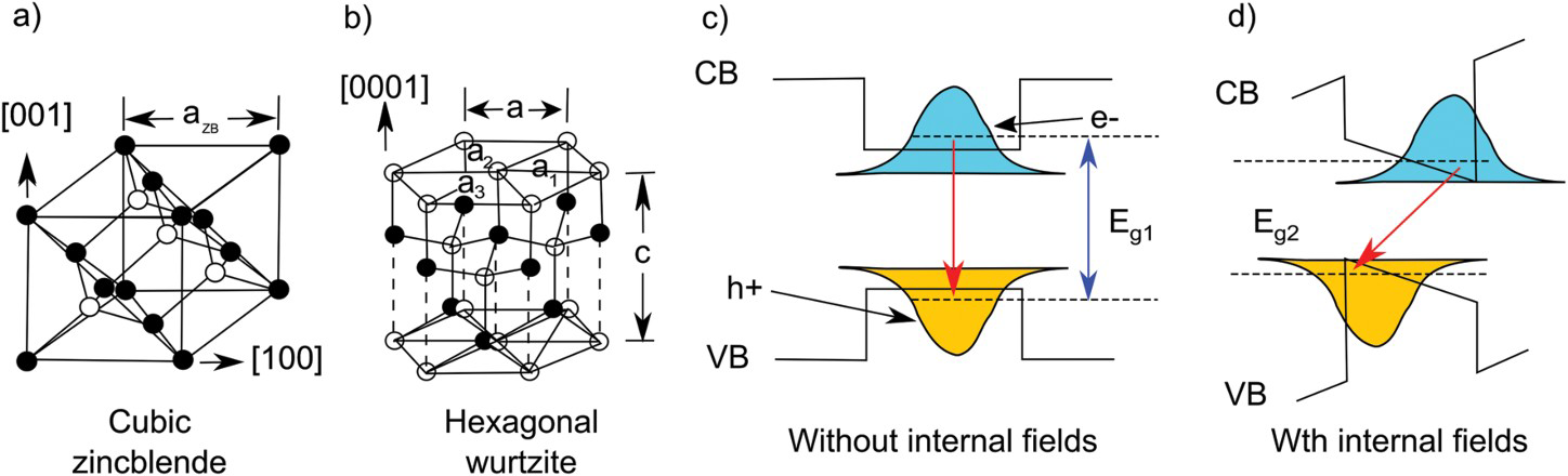
Increased indium concentrations and thickness in the InGaN quantum wells result in larger lattice mismatch and strains with the GaN quantum barriers, thus larger piezoelectric polarisation fields. Again, this results in a lower rate of radiative recombination. Moreover, with higher indium content, the density of point and extended defects increases and inhomogeneous indium concentrations are observed in c-plane wurtzite GaN [9] to result in a higher rate of non-radiative recombination. The lower rates of radiative recombination and higher rates of non-radiative recombination from the above factors result in the decrease in IQE and EQE of c-plane wurtzite GaN LEDs of decreasing wavelengths from blue to green.
Properties of cubic zincblende GaN and InGaN
The cubic zincblende ( ) structure and the hexagonal wurtzite (
 ) structure are two different crystal polytypes of the same material, differing in the arrangement of the atoms within the material. The most obvious advantage that zincblende InGaN possesses over wurtzite InGaN for green-wavelength emission is the absence of spontaneous and piezoelectric polarisation fields in the [001] growth direction, due to the nature of the crystal structures as depicted in Figure 3(a) and (b) (Hanada [7]). The lattice parameters a = b = c for zincblende, whereas a ≠ c for wurtzite. Therefore, in the zincblende structure, strains due to the lattice mismatch between GaN barriers and InGaN wells should not give rise to piezoelectric polarisation fields and the associated QCSE described previously. Additional strains from higher indium content and thicker quantum wells for green-wavelength emission also do not contribute to internal electric fields for zincblende InGaN, thus both indium content and thickness of wells can be tuned in a wider range without reducing recombination efficiency. Moreover, zincblende InGaN has a smaller band gap than wurtzite InGaN by around 0.14 eV at 300 K, as shown in Figure 2. Therefore, zincblende InGaN quantum wells require lower In incorporation compared with equivalent non-polar or semi-polar InGaN quantum wells. However, zincblende GaN is a metastable phase, while wurtzite GaN is the thermodynamically more stable phase, so careful selection and optimisation of growth conditions are required.
Zincblende GaN growth methods
GaN- and GaN-based heterostructures are grown in an epitaxial manner, where a crystalline thin film is deposited monolayer by monolayer on a crystalline substrate. The orientation and crystal structure of the thin film are determined by the substrate. Zincblende GaN has been mainly grown by molecular beam epitaxy (MBE) and metal-organic vapour phase epitaxy (MOVPE). MBE is an ultra-high vacuum technique in which the ultra-pure forms of the elements are made to sublime, by either heating or electron beam evaporation. The fine molecular beams formed in this way are directed to a heated substrate, where the atoms of the different elements become physically adsorbed and subsequently incorporated into the crystal lattice through formation of bonds with neighbouring lattice atoms. The low growth rates (50–400 nm/h for zincblende GaN) of this process notionally allow precise atomic layer control of the growth. As for MOVPE, precursors are carried into the reaction chamber by a carrier gas that becomes saturated with the precursors as it is bubbled through solutions of the precursors. In the reaction chamber, the precursors flow laminar above the heated substrate and decompose by pyrolysis to leave behind the pure elements (e.g. Ga, In and N). Like MBE growth, the pure elements are then physically adsorbed on the heated substrate and incorporated into the crystal lattice. MOVPE does not require an ultra-high vacuum and has a faster growth rate compared with MBE, hence it is widely employed in industry for the growth of commercial GaN-based LEDs.
The growth of GaN is usually heteroepitaxial, which means that the substrate is not GaN but another material, since bulk GaN substrates are not readily available and expensive. The choice of substrate is vital to ensure zincblende GaN growth. The main substrates that have been studied include cubic GaAs (001) (by MBE [10–14] and MOVPE [15–21]), 3C-SiC (by MBE [22–26] and MOVPE [27]), 3C-SiC on Si by MBE [28–33], patterned 3C-SiC on Si [34] and patterned Si [35–37] substrates. Some of the substrate properties to consider are lattice matching and difference in thermal expansion coefficient with zincblende GaN and cost. Cubic GaAs substrates and zincblende GaN have a large lattice mismatch of 20% resulting in a high density of defects in the zincblende GaN layer [38]. 3C-SiC (3C simply denotes the cubic zincblende structure of SiC) substrates have a much lower lattice mismatch of 3% with zincblende GaN which thus produces zincblende GaN with improved crystallinity and lower content of hexagonal inclusions [22,23,25]. However, the limiting factor to the success and commercialisation of the growth of zincblende GaN on 3C-SiC is the prohibitively high cost of the substrate compared with silicon substrates. By depositing only a few micrometres of 3C–SiC onto silicon substrates, as shown in Figure 4, the best of both worlds can be achieved. The commercial viability of zincblende GaN LEDs grown on such substrates is also increased by the availability of large area (up to 8 inches in diameter) Si substrates. 3C-SiC layers have been grown on silicon by chemical vapour deposition [32], carbonising with a carbon-containing gas such as C2H2 [39,40], carbonisation in rapid thermal processing reactor [31] and high-dose carbon ion implantation [33]. More recently, Stark et al. [35] and Bayram et al. [36] have both used patterned Si substrates with {111} side walls, although in slightly different geometries. Referring to Figure 5, the hexagonal wurtzite GaN phase first nucleates on the two opposite {111} side walls, and the zincblende phase forms where the two wurtzite crystals meet [35]. Such methods result in stripes of zincblende GaN crystal being formed, with a width of ∼1 µm and a length limited by the size of the substrate.
Zincblende GaN epilayer grown by MBE on thin Coalescence of the two wurtzite crystal nucleated at the Si {111} side walls results in the formation of zincblende GaN phase. Reprinted from Stark et al. [35], with the permission of AIP Publishing. -SiC/Si (001) substrates. Reprinted from As et al. [31], with the permission of AIP Publishing.
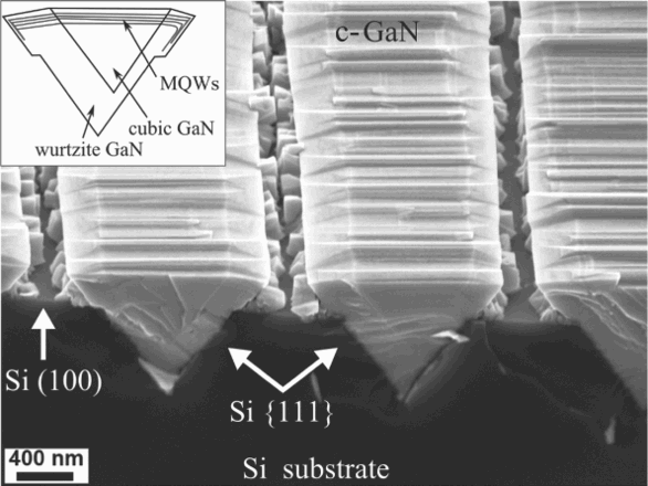
Thin film growth of zincblende GaN typically consists of several steps. After annealing and cleaning of the substrate, a porous nucleation layer of a few nanometres is often grown at around 600°C [24,31,41–43] that compensates the lattice mismatch with the substrate. An annealing and crystallisation step is used to smoothen the nucleation layer, before a thicker buffer layer of several hundred nanometres is grown. The substrate temperature during subsequent GaN growth can affect the kinetics of the growth surface and is important in controlling the polytype of GaN that nucleates on the surface. Zincblende GaN is typically reported to be stabilised at lower temperatures of 600–950°C, compared with 1000–1100°C for wurtzite GaN. Moreover, the substrate temperatures reported for MOVPE (900–950°C) [16,42,44,45] are generally higher than those of MBE (600–835°C) [29–31,33,43,46,47]. The ratio of N to Ga, or V/III ratio, can affect surface diffusion since N adatoms have a higher sticking coefficient than Ga adatoms [39]. A high V/III ratio can thus limit surface diffusion and promote surface roughening, which has been reported to subsequently result in the nucleation of hexagonal inclusions [31,47]. Typical optimised V/III ratios used for MOCVD zincblende GaN growth are 1000–1500 [19,42].
Wurtzite inclusions
The aim of optimisation of growth conditions is to minimise the amount of wurtzite inclusions. The stacking sequence of the close-packed planes in the wurtzite structure is ABABABAB, while that of the close-packed {111} planes in the zincblende structure is ABCABCABC. A stacking fault in the zincblende structure arises when the stacking sequence is disordered to become ABCA
Crystal defects
Stacking faults in zincblende GaN have been consistently found to lie on the {111} planes when grown on both GaAs [49,50], 3C-SiC [26,32] and patterned 3C-SiC/Si [34] substrates. The prevalence of stacking faults in zincblende GaN is likely due to stacking faults having the same stacking sequence as the wurtzite structure, which is more thermodynamically stable than the zincblende structure. Wang et al. [39] found that many stacking faults originate from the rougher regions of the interface between the zincblende layer and a 3C-SiC/Si substrate. However, it is not clear if the stacking faults originate at the substrate surface steps, at existing stacking faults in the substrate, or at other locations. It is important to understand the origin of stacking faults to reduce their densities. The stacking fault density is found to decrease with the distance from the GaN/substrate interface by Martinez-Guerrero et al. [32], and it has been suggested that stacking faults lying on the {111} planes in the zincblende structure can intersect and annihilate to create a sessile dislocation in the <110> directions.
The light-emitting MQW active region (refer to Figure 1) is arguably the most important part of an LED structure. The effect of stacking faults on the confinement of electrons and holes, and radiative and non-radiative efficiencies of the MQW region are so far not well understood. Kemper et al. [51] reported that stacking faults on the {111} planes in zincblende GaN led to a decrease of the scanning transmission electron microscopy-cathodoluminescence emission intensity. This seems to indicate that stacking faults reduce radiative recombination efficiencies, although it is possible that there is also a corresponding decrease in dislocation density with increasing thickness of GaN films that can also decrease radiative recombination efficiencies. In wurtzite GaN, zincblende stacking faults are thought to act as type–II quantum wells [52,53]. Since zincblende GaN has hexagonal wurtzite stacking faults, it is possible that stacking faults in zincblende GaN have similar type-II quantum well emission properties. Moreover, Kemper et al. [48] reported that stacking faults resulted in MQWs with an undulating morphology; however, whether this affects light emission properties still needs to be investigated. An obvious and simple remedy to avoid the effects of stacking faults is to grow thicker GaN films to reduce the stacking fault density near the MQW light-emitting region of the LED.
Owing to the lattice mismatch between GaN and the substrates, structural defects, such as misfit dislocations, stacking faults and microtwins, have been attributed to relieving strain at the interface [48,54]. Pure edge-type misfit dislocations occurring at regular intervals (every fifth {111} lattice plane of zincblende GaN grown on GaAs substrate) by Trampert et al. [54]. were revealed with high-resolution TEM. With a low formation energy in fcc crystals [55], it is questionable whether stacking faults help to relieve strain. Twinning has been reported for zincblende GaN grown on GaAs [50,54,56]; however, the mechanism by which strain is relieved is not clear.
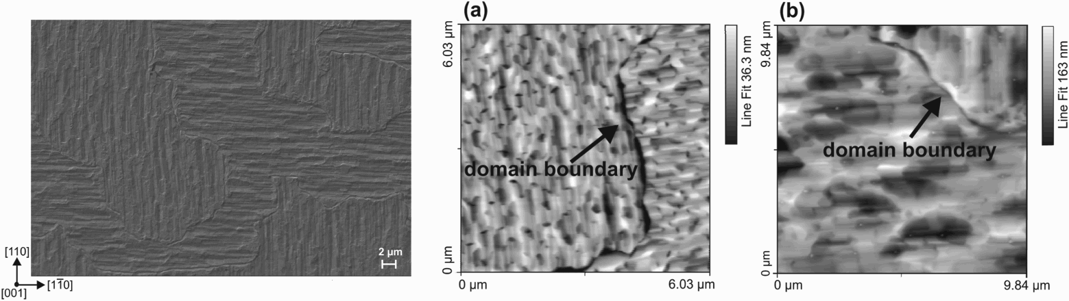
Antiphase domains present in 3C-SiC/Si substrates can template on to subsequent zincblende GaN growth, as observed by Kemper et al. [57], as shown in Figure 6. A silicon substrate is not atomically flat and exhibits surface steps. Figure 7(a) and (b) schematically illustrate two neighbouring nuclei that have nucleated on different steps of step height SEM (a) and AFM (b) images of antiphase domains in zincblende GaN. Reprinted from Kemper et al. [57], with the permission of AIP Publishing. (a) and (b) Schematic of two neighbouring 3C-SiC nuclei that have nucleated on different steps of a stepped (001) Si substrate. The height between the two steps is  . If n is odd, the two nuclei have an antiphase relationship between them and an antiphase boundary results. If n is even, the two nuclei do not have an antiphase relationship and only a vertical displacement boundary results. Antiphase domains in 3C-SiC layers template the subsequent growth of zincblende GaN [57] and can result in lattice defects such as stacking faults in subsequent growth of GaN [58]. It is well known that introducing a miscut to the substrate by cutting the Si wafer at a slight angle (< ∼ 5°) reduces the presence of antiphase domains in GaAs [59] and Si [60]. Huang et al. [60] proposed that the double step height, h1 was critical for achieving antiphase domain suppression on the miscut Si substrate.
 , where in (a) n = 1 and in (b) n = 2. It is assumed that SiC is more thermodynamically stable than Si and that the first layer that is deposited on the silicon (white circles) surface is a layer of carbon atoms (black circles). ‘DB’ and ‘APB’ are ‘displacement boundary’ and ‘antiphase boundary’, respectively. Reprinted from Pirouz et al. [58], with the permission of AIP Publishing.
Doping of zincblende GaN
Doping basics
GaN is doped to create mobile electrons and holes that can be injected into the MQW active region for radiative recombination. Doping generates donor and acceptor energy levels within the band gap of GaN, as shown in Figure 8, and donors and acceptors need to be ionised (usually thermally) to generate electrons and holes. Donors (acceptors) can be identified as shallow or deep depending on how close or far their energy levels are from the conduction (valence) band. P-type doping of GaN to generate holes can be achieved by replacing the group III gallium site with a group II element (e.g. Mg) or the group V nitrogen site with a group IV (e.g. C). On the other hand, n-type doping to generate electrons can be achieved by replacing the gallium site with a group IV element (e.g. Si) or the nitrogen site with a group VI element.
Energy level diagram showing acceptor, donor and deep donor states. The arrows going across the energy levels represent various radiative recombination mechanisms: (1) free excitons or near band edge emission, (2) from conduction band to shallow acceptor state, (3) from conduction band to deep acceptor state.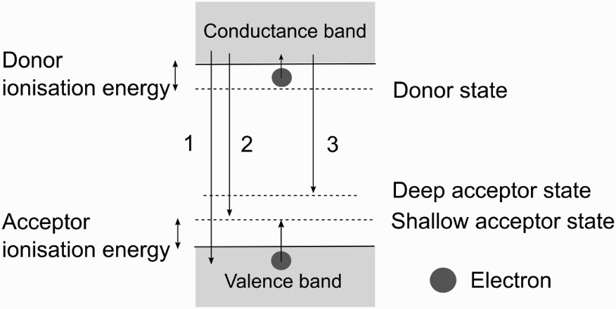
The degree of p-type and n-type dopant incorporation can be determined from secondary ion mass spectroscopy (SIMS) measurements. Carrier concentration and mobility are usually measured through Hall effect measurements with the Van der Pauw method. Finally, the ionisation energy of a dopant is often determined from photoluminescence (PL) spectroscopy, where the sample is optically excited by a laser and the emission energy and intensity of subsequent radiative recombinations are detected. Peaks can be assigned to radiative recombination mechanisms by comparing with spectra from known samples or with theoretical predicted values.
P-type doping
Magnesium doping
Mg concentrations and corresponding hole concentrations and mobilities reported in studies of Mg-doped zincblende GaN epilayers.
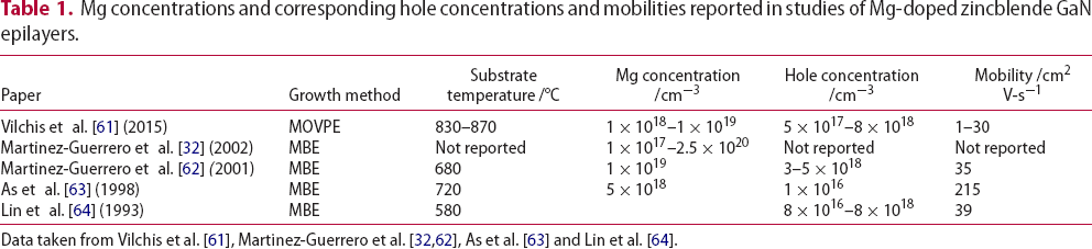
Data taken from Vilchis et al. [61], Martinez-Guerrero et al. [32,62], As et al. [63] and Lin et al. [64].
The Mg-doped zincblende GaN epilayers grown by MOVPE from Vilchis et al. [61] have a much higher ratio of hole to Mg concentrations compared with those grown by MBE from Martinez-Guerrero et al. [62] and As et al. [63]. To explain the low hole to Mg ratios for MBE-grown epilayers, it was suggested that background oxygen concentrations from the Mg source resulted in Mg having to compensate the n-type doping, and the formation of Mg complexes and precipitates [32]. It is possible that MOVPE produced higher quality epilayers with fewer structural defects, which trap impurities, [62] compared with MBE to result in more ionised Mg. The composition of wurtzite inclusions of optimised epilayers by Vilchis et al. [61] is less than 5%; however, there are no further structural studies from Vilchis et al. [61], Martinez-Guerrero et al. [62] and As et al. [63] to confirm the connection between defects and ionisation of Mg. Future studies correlating Mg concentration to structural defects, presence of Mg complexes or precipitates and background oxygen levels of Mg-doped zincblende GaN layers will be useful.
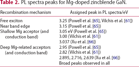
PL spectra peaks for Mg-doped zincblende GaN.
Several authors [32,63,64] have reported the tendency for Mg to segregate towards the surface of the Mg-doped zincblende GaN films at such Mg concentrations, with Lin et al. [64] suggesting that a possible cause is the difference in covalent radius between Mg and Ga. As et al. [63] also observed Mg segregation towards the GaN/GaAs substrate interface that could be due to increased Mg diffusion into GaAs or the high density of defects near the interface.
Another problem, which applies mainly to MOVPE growth, is the formation of neutral H-Mg complexes. Since hydrogen is generally present in a MOVPE reactor, either as a carrier gas or an impurity in precursors, it is likely to incorporate into the thin film to form H-Mg complexes. Thermal annealing at 700–900°C is usually used for Mg-doped wurtzite GaN to activate neutral Mg-H complexes to form Mg acceptors, by providing the energy and time for the complex to dissociate and H to diffuse out of the structure [6]. However, Vilchis et al. [61] reported that no thermal annealing was required for MOVPE-grown Mg-doped zincblende GaN, based on a study by Guarneros et al. [68] on similar Mg-doped wurtzite GaN films that showed no increase in hole concentrations with annealing. A high Mg to hole concentration ratio was obtained by Vilchis et al. [61], and it is possible that the growth temperature of 830–870°C (around the annealing temperatures used for wurtzite Mg-doped GaN), long growth time of 60 mins and thin film of 1 µm allowed most of the H to dissociate and diffuse out. As et al. [69] also reported that no annealing step after the growth of Mg-doped zincblende GaN was necessary without providing reasoning, but the Mg-doped zincblende GaN films were grown by MBE in ultra-high vacuum with an absence of a hydrogen source.
Carbon doping
Owing to the difficulties with magnesium p-type doping, a few studies have investigated p-type doping of zincblende GaN by carbon [70–72]. Carbon is a group IV element, which can either replace the group V nitrogen site as an acceptor or the group III gallium site as a donor, resulting in potential amphoteric behaviour. Since carbon is more similar to nitrogen in atomic radius and electronegativity, it is expected to replace the nitrogen site instead of the gallium site.
Carbon doping has been achieved through electron beam evaporation of a graphite rod [70] and sublimation of solid CBr4 powder [71,72]. The maximum carbon incorporation concentrations were 2 × 1020 cm−3 from As et al. [70] and 1 × 1020 cm−3 from Zado et al. [72] before the zincblende GaN film degraded in quality. The two authors who studied carbon doping of zincblende GaN each identified factors to explain the observed variation in hole concentrations with flux of carbon. With increasing electron beam power on the carbon source, As et al. [70] observed an initial rise of hole concentration to a maximum of 6 × 1017 cm−3 before a dramatic decrease, which suggested the introduction of compensating centres at high carbon flux. It is also possible that the amphoteric nature of carbon causes carbon to act as a p-type dopant at low carbon flux and n-type dopant at higher carbon flux with increasing electron beam power on the graphite rod; however, Zado et al. [72] did not observe tendency towards n-type behaviour with increasing carbon incorporation. Instead, the net donor concentration decreased before the net acceptor concentration increased to a maximum of 1 × 1019 cm−3, as shown in Figure 9. The result was explained by the carbon atoms first compensating unintentional n-type doping of the undoped layer, possibly due to oxygen from the nitrogen source for GaN, before acting as acceptors. It is difficult to compare the results from As et al. [70] and Zado et al. [72] directly since the two sources of carbon are different, which might affect the mechanism of incorporation of carbon into the zincblende GaN layers.
As carbon concentration in an undoped zincblende GaN film increased (diamonds), carbon first compensated the unintentional n-type doping (squares show net donor concentration), before acting as an acceptor to result in p-type doping (circles show net acceptor concentration). Reprinted from Zado et al. [72], with the permission of Elsevier.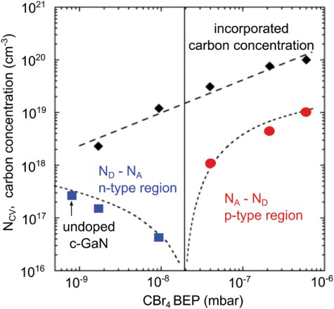
Overall, the results from the three initial studies of carbon p-type doping seem encouraging for further investigation, with questions that include whether hole mobilities are improved compared with magnesium doping, and whether the amphoteric nature of carbon dominates above a certain degree of incorporation.
N-type doping
Traditionally, the group III element Si is used for n-type doping in wurtzite GaN, due to the similar size of Ga and Si ions resulting in a high incorporation efficiency of Si on Ga-sites. Moreover, the shallow donor ionisation energy of Si in wurtzite GaN leads to high concentrations of free carriers with high mobilities at room temperature. Owing to the similarities between wurtzite and zincblende GaN, similar doping properties can be expected when using Si as n-type dopant.
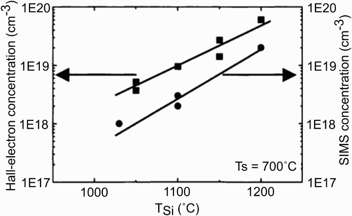
The Si and electron concentrations reported by studies of Si-doped zincblende GaN layers are plotted in Figure 10. The Si concentrations (1 × 1018 cm−3 to 1 × 1020 cm−3) and electron concentrations (2 × 1018 cm−3 to 3.9 × 1020 cm−3) are both higher compared with Mg and hole concentrations, and in the case of Martinez-Guerrero et al. [62], the electron concentration is actually higher than the Si donor concentration. The two following factors described can help explain these observations. First, the electron concentration of Si-doped zincblende GaN layers was found to follow the Si concentration curve, as shown in Figure 11, which indicates that most of the Si atoms are located on the Ga sites and ionised [62,75]. Second, unintentional n-type doping can increase the overall electron concentration, either by Si that diffuses from an underlying SiC substrate into GaN layer (typical unintentional Si doping is 2–7 × 1017 cm−3) [62], or by oxygen (e.g. from NH3 nitrogen source) since Xu et al. [73] reported that undoped GaN grown on GaAs substrate by MOVPE has an electron concentration of 1 × 1017 cm−3.
Electron concentrations (squares) from Hall measurements and Si concentrations (circles) from SIMS of Si-doped zincblende GaN films grown on SiC/Si (001) substrate. Reprinted from Martinez-Guerrero et al. [62], with the permission of Elsevier.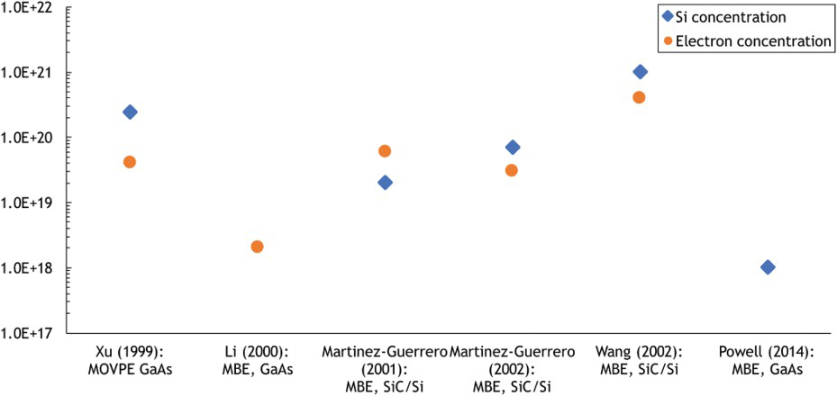
There has been concern whether high concentrations of Si incorporation lead to defects and wurtzite inclusions in the zincblende GaN layers. {111} stacking fault density was reported to increase with Si incorporation when Wang et al. [40] compared reflection high-energy electron diffraction (RHEED) patterns and cross-sectional TEM micrographs of undoped and Si–doped layers with Si concentration of 1 × 10¹⁹–1 × 1021 cm−3. By comparing samples of varying Si concentration, Xu et al. [73] attributed the UV 364 nm emission peak of the room temperature PL spectrum of a film with Si incorporation of 4 × 1019 cm−3 to the wurtzite phase. Since stacking faults are essentially wurtzite inclusions in zincblende GaN and often thought to act as nucleation sites for the wurtzite phase, the interpretations of the presence of stacking faults by Wang et al. [40], and wurtzite phase by Xu et al. [73] of Si-doped zincblende GaN layers support each other.
The dislocation density of Si-doped sample with a high Si concentration (1 × 1021 cm−2) was found to be ∼1 × 109 cm−2, mostly at small-angle grain boundaries within the grains, while the dislocation density of the undoped sample was ∼5 × 108 cm−2 found mostly at grain boundaries from plan-view TEM images by Wang et al. [40]. However, at lower Si concentrations between 1019 and 1020 cm−3, Martinez-Guerrero et al. [32] reported that the FWHM of an X-ray diffraction ω-scan showed similar values of mosaicity (misorientation of different crystallites within the film), which means the Si-doped layers should have similar dislocation densities.
Li et al. [76] claimed that the broadening of FWHM of PL spectra of c-GaN as a function of Si doping concentration was due to the microscopic fluctuations of doping concentration. However, it is unclear what sort of length scales the author means for the fluctuations, nor is there more direct evidence of such doping fluctuations.
With the variety of defects that seem to accompany Si incorporation into zincblende GaN films, it will be useful to understand the extent of their effects on the mobility of electrons.
Zincblende InGaN on GaN heterostructures
The ability to form InGaN on GaN heterostructures is vital for the light-emitting InGaN/GaN MQW region of an LED. In terms of the interfaces within the zincblende InGaN/GaN MQWs, Li et al. [77] and Kitamura et al. [43] concluded that the interfaces have high structural qualities, with X-ray diffraction superlattice satellite peaks up to fifth order. Within zincblende InGaN films, several authors reported the presence of In-rich phases [78,79] or phase-separated quantum dots [80], and suggested the cause to be the spinodal decomposition of InGaN. Such films studied were thick (300 nm) and therefore relaxed, which is not particularly relevant to LEDs where InGaN layers are thin (typically <10 nm) and biaxially strained.
In order to investigate the effect of biaxial strain, Tabata et al. [81] performed calculations of mixing free energy for zincblende InxGa1−xN alloy as a function of composition at a temperature range between 700 and 1100 K, for both fully relaxed and biaxial-strained films. Results predicted for films with x ≅ 0.4 that spinodal decomposition would take place on relaxed films but be suppressed on biaxial-strained films. Subsequently, Tabata et al. [81] compared the micro-Raman spectra of thin (3 nm) layers to thicker (30 nm) layers, which correspond to strained and relaxed layers notionally, between a 400 nm GaN buffer layer and 30 nm GaN cap. The thinner layers did not show the peak corresponding to the In-rich phase (x ≅ 0.5–0.6) present in relaxed layers, even though they were annealed so that total time at growth temperatures was similar as for thicker layers, giving rise to the conclusion that biaxial strain suppressed spinodal decomposition in InGaN quantum wells. However, it might be the case that the strained layers used are so thin (3 nm) in the study that the Raman measurements do not pick up the presence of any In-rich phase. Pacheco-Salazar et al. [82] also claimed that the minute volume taken up by the In-rich phase means that only PL measurements can detect their presence due to high recombination efficiency of the In-rich phase, but not by other optical methods such as Raman spectroscopy. Moreover, Husberg et al. [83] found the 30 nm In0.56Ga0.44N layer between a 300 nm GaN buffer and 30 nm GaN layer to be strained instead of relaxed through high-resolution X-ray diffraction measurements, in contrast to Tabata et al. [81]. The InGaN layer also showed evidence of an In-rich phase (x = 0.56) through PL measurements and reciprocal space map from X-ray diffraction.
Using first principles total energy calculations, Teles et al. [84] showed that biaxial strain suppresses spinodal decomposition of InGaN alloys by encouraging the formation of ordered [n,m] superlattices consisting of n planes of In and m planes of Ga stable up to 1000 K, with the [3,3] superlattice at x ≅ 0.5 having the lowest excess energy. Therefore, Teles et al. [84] believe that the In-rich phases (x = 0.56) reported by Husberg et al. [83] could be such an ordered structure of InGaN; however, the reciprocal space map from X-ray diffraction does not show oscillation fringes that would be expected from the periodic structure. No stable ordered structure was found for thick unstrained InGaN alloys, hence spinodal decomposition is predicted to occur as mentioned in Silveira et al. [78], Tabata et al. [79] and Lemos [80]. The direct observation of such ordered InGaN structures and their effects on localisation of carriers and light emission properties have yet to be investigated.
Zincblende AlGaN on GaN heterostructure
AlN has the largest band gap in the III-nitrides and, if alloyed with GaN, results in AlGaN that has a larger band gap than InGaN. Therefore, AlGaN with low Al content would be useful as confinement and electron blocking layers (refer to Figure 1) for zincblende GaN LEDs, similar to wurtzite GaN LEDs. In wurtzite GaN LEDs, electron blocking layers are usually made from higher Al content AlGaN layers to create an even higher band gap layer, since the diffusion constant and hence leakage current of electrons are usually greater than holes in III-V semiconductors [85]. An alternative is to use AlxIn1−xN, which has a larger band gap compared with InGaN and GaN at all x compositions with the possibility of providing very close lattice matching, as shown in Figure 2.
So far, there is no known literature on AlGaN on GaN as an electron blocking layer in zincblende GaN LEDs. Instead, studies on zincblende AlGaN have been performed for AlGaN epilayers [86,87], AlN/GaN MQWs [26], AlGaN/GaN tunnel diodes [88], distributed Bragg reflectors [89] and laser diodes [90]. No major issues with the growth of such AlGaN/GaN heterostructures, such as phase separation, wurtzite inclusions and lattice matching, were reported. Zainal et al. [88] used in situ RHEED, and ex situ X-ray diffraction and PL to confirm the presence of high-quality zincblende GaN and Al0.3Ga0.7N layers with negligible wurtzite inclusions, while Li et al. [89] found no cracks for the 15.5 layer-stacks of c-Al0.3Ga0.7N/GaN, where the thicknesses of the AlGaN and GaN layer were 55 nm and 52.7 nm, respectively, from scanning electron microscopy.
Optical properties of zincblende InGaN/GaN quantum wells
The optical properties of zincblende GaN-based structures ranging from simple p-n junctions [18,30,69], to MQWs [77], to full LED structures [35] have been reported. Since one of the major motivations for zincblende GaN is to produce efficient LEDs that emit green wavelengths, it is encouraging that Li et al. [77] showed strong green (520 nm) PL emission from InxGa1−xN/GaN six-period MQWs [77]. In theory, zincblende GaN MQWs should have an absence of internal polarisation fields along the (001) growth direction. Li et al. [77] and Stark et al. [35] provided results that supported this. For wurtzite InGaN/GaN MQWs, as the quantum well thickness increased, PL intensity was observed to decrease due to larger internal electric fields separating the electrons and holes [91]. On the other hand, Li et al. [77] observed that PL intensity increased with quantum well thickness for zincblende InGaN/GaN MQWs. Stark et al. [35] showed that the peak wavelength of the electroluminescence spectra of zincblende InGaN/GaN MQWs remained constant as current density was increased, while the peak wavelength for wurtzite LEDs usually shifts. The internal piezoelectric and spontaneous electric fields result in larger band bending of wurtzite InGaN quantum wells compared with those with zincblende structure. If the current density across the wurtzite LED increases, the electron and hole wavefunctions across a quantum well shift and become more spread out, resulting in overlap across different band gap energies and shift in peak wavelength of the electroluminescence spectra. For the zincblende LED, the band bending of an InGaN quantum well is not as severe, hence an increase in current density does not result in pronounced shifts in carrier wavefunction peaks and their overlap.
Other issues related to zincblende GaN-based LEDs
Diode leakage
Several studies [18,30,35,69] have reported leakage currents when the structures are under reverse bias, at voltages as low as − 3 V [30]. There are different opinions regarding the cause of such leakage currents. For p-n junctions formed from Mg-doped p-type GaN and Si-doped n-type GaN, Gamez-Cuatzin et al. [30] and As et al. [69] suggested deep levels in the band gap resulted in the leakage currents. From room temperature electroluminescence spectra, Gamez-Cuatzin et al. [30] and Yang et al. [18] observed a blueshift in the luminescence peak with increasing injection current and attributed this to the saturation of deep states. PL at 10 K showed a broad 2.8 eV band associated with deep Mg states, and the electroluminescence spectra showed an increasing Mg-related blue band (between 2.5 and 2.8 eV) at higher temperatures as Mg deep levels are ionised [30]. Yang et al. [18] also reported the blue (∼2.8 eV) peak that dominated in a room temperature electroluminescence spectrum. However, As et al. [69] did not observe the blue Mg-related band in a room temperature electroluminescence spectrum. Instead, the leakage current and deep levels were attributed to the large dislocation density (∼1010 cm−2) in the GaN layer.
Contacts
Low resistance Ohmic contacts are vital to connect the n-type and p-type layers of an LED structure to an external power source for forward biasing. An Ohmic contact has a negligible potential barrier to carriers flowing in either direction between the metal and semiconductor. This is as opposed to a Schottky contact which has a significant potential barrier and is undesirable for LEDs. The formation of an Ohmic contact is influenced by the following factors: the work functions of the metal and zincblende GaN and resultant band bending of the semiconductor, Fermi level pinning by surface states, and tunnelling effects from a thin contact or heavy doping of the semiconductor.
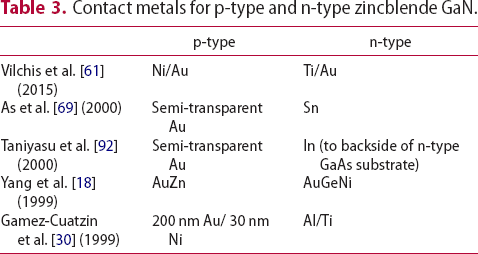
Contact metals for p-type and n-type zincblende GaN.
Internal and external quantum efficiencies (IQE and EQE)
With the lack of full LED structures based on zincblende GaN, the IQE and EQE of such devices have yet to be investigated, although Stark et al. [93] calculated the IQE of an LED grown on v-grooves of Si (001) substrate to be a maximum of 36% from ratio of intensity of CL peaks at 78 K and 300 K. The calculation assumes IQE to be close to 100% at the low temperature, but the assumption is not entirely valid as non-radiative recombinations still exist at such low temperatures [94]. Since much of the more recent research is focused on zincblende GaN grown on Si-based substrates, it is worth bearing in mind that the Si substrate needs to be removed to allow light extraction from the LED. This is evident from the low EQE of 3 × 10⁻⁵ reported by Stark et al. [35] of an LED grown on v-grooves of Si (001) substrate.
Concluding remarks
Zincblende GaN offers an alternative pathway to solving the ‘green gap’ problem, distinct from wurtzite GaN in semi-polar and non-polar orientations. The growth of zincblende GaN on 3C-SiC/Si and wurtzite GaN on Si patterned substrates appear promising, with good lattice matching with zincblende GaN and high commercial viability of Si-based substrates. It is now important to gain a deeper understanding of defects present in zincblende GaN, such as stacking faults and dislocations, including their origin, effects on light emission and elimination methods if required. P-type and n-type doping levels of zincblende GaN are comparable to levels in wurtzite GaN. For p-type doping, Mg incorporation and the ratio of Mg/hole concentrations can still be improved, although there is also the possibility of p-type doping by carbon to be explored further. As for n-type doping, defects resulting from high Si incorporation need to be controlled if they are found to hinder the mobility of electrons. The non-uniformity of In content within InGaN layers reported, with the possibility that they are ordered structures, need to be better understood. With evidence supporting the absence of internal electric fields in zincblende GaN structures, which is a major motivation for zincblende GaN research, the path ahead towards a successful zincblende GaN green-wavelength LED seems worthy of efforts, despite the above challenges that need to be addressed.
Footnotes
References
 -SiC/Si (001) substrates
 -GaN films
 -SiC
-SiC