
Abstract
Cu–Ni–Si alloys exhibit a good combination of strength and electrical conductivity and may be a potential candidate for utilisation in electrotechnical applications. In this work, the mechanical behaviour and its relation to the microstructure of a Cu–Ni–Si alloy, subjected to different solution heat treatment cycles, were investigated. Tensile, bend and hardness testing, in addition to Optical and Scanning Electron Microscopy, were employed, as the main analytical techniques, in the context of the present investigation.
This paper is part of a Thematic Issue on Copper and its Alloys.
Introduction
High-conductivity materials are important for electrotechnical applications in sectors such as the automotive, robotic, and electronic industries. Therefore, a wide range of low-alloyed precipitation-hardened copper alloys is potential candidates for these industrial fields, such as the Cu–Cr, Cu–Cr–Zr, Cu–Fe–P, Cu–Ni–Zn, Cu–Ni–Sn and Cu–Ni–Al systems [1-8] due to their combination of mechanical and electrical properties [9]. However, Cu–Ni–Si alloys present significant interest since, both their mechanical and electrical properties, are quite elevated and therefore could pose an ideal alternative [10,11].
Cu–Ni–Si alloys are widely used in the production of Integrated Circuit (IC) lead-frames and other relevant products demanding a good combination of strength and high electrical conductivity [12,13]. Depending on their thermomechanical processing and chemical composition, such alloys may reach high Ultimate Tensile Strength UTS (>1000 MPa) and high electrical conductivity (>25% International Annealed Copper Standards, IACS) values [12,14]. They were first developed in 1927 by Corson, who attributed the strengthening of the material to the precipitation of fine orthorhombic δ-Ni2Si particles during aging [15-17]. According to the relevant literature, several intermetallic compounds (Ni x Si y ) have been observed in the Cu–Ni–Si system [18-25] from which δ-Ni2Si is considered the most thermodynamically stable phase [19]. However, since the precipitated phases are very fine (10–50 nm), their characterisation and distinction are challenging even with the use of a Transmission Electron Microscope [26]. It has also been observed that an optimal strength-conductivity ratio is achieved for an atomic ratio of Ni–Si equivalent to 2/1 with respect to the chemical composition [12]. Lastly, additions of Mg have been found to decrease the inter-particle spacing of the δ-Ni2Si precipitates while also decelerating the dislocation motion due to Mg-atom drag according to the Orowan strengthening mechanism, resulting in an increase of the alloys’ strength [27,28].
To the best of our knowledge, there is a lack of information on the solution treatment process of Cu–Ni–Si alloys in international literature and therefore, a relevant study could provide an insight on the process parameters and their effects on the achieved microstructure and mechanical properties. This knowledge will serve as a significant predecessor of the optimisation of the subsequent aging treatment process, aiming to improve the properties and functionality of the final product. Cold rolled Cu–Ni–Si alloy sheets containing <5.0 at-.% Ni and <2.5 at.-% Si are typically solution-treated at temperatures over 850°C and, then, quenched in water followed by aging treatments at temperatures between 400 and 500oC [25]. Therefore, the selection of an appropriate combination of temperature and time for the solution heat treatment process is of substantial importance since precipitation may occur during hot-forming or even during severe cold working, where dynamic intergranular precipitation has been reported [26].
This research reveals the effect of the solution treatment duration on the microstructure and mechanical properties of a 0.4 mm thick Cu–Ni–Si strip. The examined material's chemical composition ranged between 2.0 and 2.5 wt-% Ni, 0.4–0.6 wt-% Si.
Mechanical properties determination including tensile testing, bending and microhardness measurements, optical (OM) and electron microscopy (SEM) characterisation along with electrical conductivity measurements were employed to assess the evolution of material properties as a function of the solution treatment feed rate, a parameter that controls the soaking duration in the annealing furnace.
Experimental procedure
Materials and processing
In the current study, 10 different CuNiSi samples were utilised for mechanical testing, microstructural examination and electrical conductivity inspection. These samples were extracted from different sample groups exposed to different final solution treatments performed after cold rolling up to 0.40 mm. The solution treatments were realised in an industrial continuous annealing furnace, at constant soaking temperature, but under varied feed rates, i.e. feedstock speeds (expressed in m min–1). The higher the feed rate, the lower the soaking duration to the solution treatment temperature. It should be noted that the annealing feed rates are properly codified in increasing order as it is shown in Figure 1. The exact values of feed rates and soaking temperature are withheld due to confidentiality issues. Schematic representing the sequence of the annealing feed rates. The feed rate of J-code is approximately nine times higher than the feed rate of A-code.
Mechanical testing and electrical conductivity measurements
Tensile testing at ambient conditions according to EN ISO 6892-1 standard was conducted using an ‘Instron 5567’ electromechanical testing machine with a 30 kN load cell and a clip-on ‘Instron 2630-113 extensometer’ with a 50 mm gauge length. Triplet tensile specimens were extracted and tested parallel to the rolling direction for repeatability purposes. The flexure resistance was evaluated employing manual bending of 25 × 50 mm flat specimens and the cracking susceptibility was ranked in respect to the bending angle (180o), transverse and parallel to the rolling direction, using a ‘Nikon SMZ 1500’ low power stereomicroscope. Hardness testing was performed with Vickers method using 1.96 N applied load employing a ‘TIME 1000 microhardness testing device’. Electrical conductivity tests were performed using a ‘Foerster Sigmatest D 2.0687 conductivity meter’, based on eddy current principle.
Optical microscopy
Microstructural examination was conducted in longitudinal sections after fine polishing and etching using a 5 g FeCl3 + 50 mL HCl + 100 mL H2O solution according to ASTM-E407 standard. Metallographic studies were performed using a ‘Nikon Epiphot 300 inverted metallographic microscope’ with bright field illumination. Grain size was measured according to ASTM-E112 using image analysis software (Image Pro Plus).
Scanning electron microscopy (SEM)/energy dispersive X-ray spectroscopy (EDS)
High magnification microstructural observations and fractographic evaluation were conducted in representative samples, utilising a ‘FEI XL40 SFEG SEM’ at 20 kV acceleration voltage, using secondary electron imaging. Electron backscatter diffraction (EBSD) analysis was performed on samples A and J with an ‘EDAX Hikari XP EBSD’, high-speed camera, on the longitudinal cross-sections (rolling direction coincides with TD and normal direction with RD coordinates) for revealing orientation of the Cu crystals and determination of preferred texture components resulting from the applied manufacturing process. EBSD scans were collected using hexagonal grid with 0.6 µm step over a 180 × 180 µm2 area resulting in ∼100k individual orientation measurements (Sample A) and using hexagonal grid with 0.4 µm step over a 72 × 72 µm2 area resulting in ∼40k individual orientation measurements (Sample J). The SEM conditions for the scans were 70o tilt position, magnification of 400× (Sample A) and 1000× (Sample J), accelerating voltage of 20 kV at working distance 10 mm. Post processing was applied to clean up the data (grain dilation).
Results
Microstructure
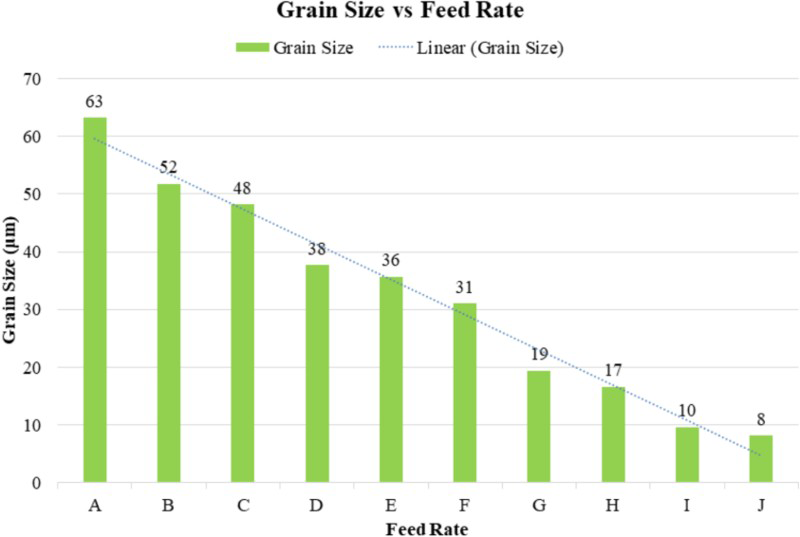
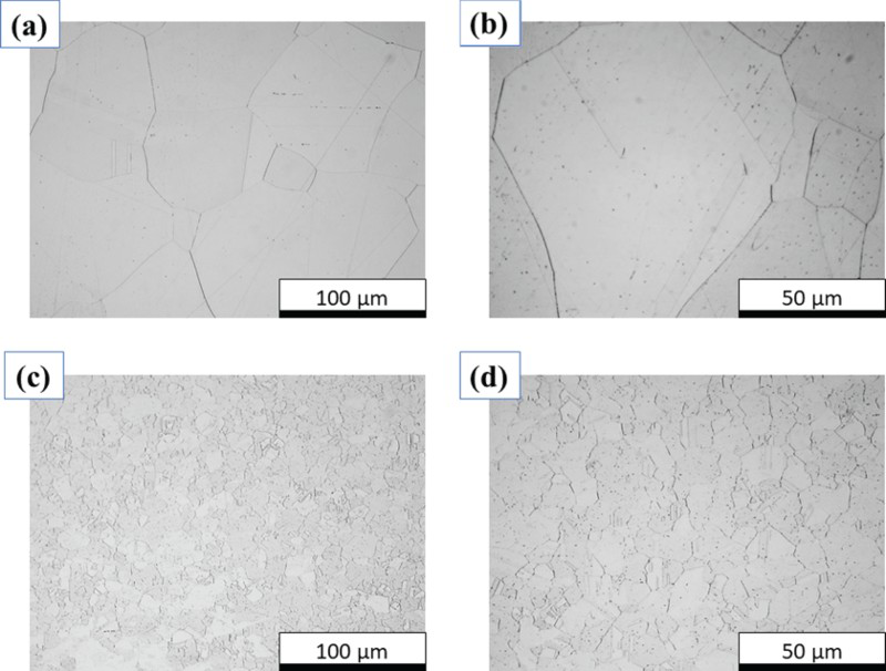
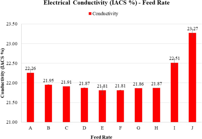
A fully recrystallized grain structure was observed for the entire spectrum of the feed-rate conditions consisting of uniform equiaxed grains exhibiting typical annealing twins (see Figure 2). Second-phase intermetallic particles were present, having an appearance of ‘dark dots’ dispersed within the Cu matrix. Grain size showed an increasing tendency (ranged from 8 to 63 µm) with a decreasing feed-rate, which is expected by the increased duration of the solution treatment (Figures 2–4). The gradual grain coarsening is a strong potential contributor to a lower elongation and bending performance. The electrical conductivity values do not change drastically for the A–H feed rate intervals exhibiting only a mild increase for A. However, for the feed rates I–J, higher conductivity values were observed (Figure 5). Microstructure and grain size under different solution treatment feed rate conditions. Evolution of the mean grain size in µm (Y-axis) vs. solution treatment feed rate (X-axis). Microstructure of sample A (a and b) and sample J (c and d). Evolution of electrical conductivity (Y-axis) as a function of feed rate (X-axis). Error bars correspond to ±1 s (standard deviation).
SEM micrographs of samples A and J, which represent the two extreme cases, are presented in (Figure 6). A discontinuous intergranular and intragranular precipitation of non-coherent Ni–Si containing intermetallic particles was observed, see Figures 4 and 6. Sample J exhibited a higher precipitates density of sphere and rodlike morphology while only spheroidized precipitates were observed in sample A. SEM micrographs of the sample (a) A and (b) sample J.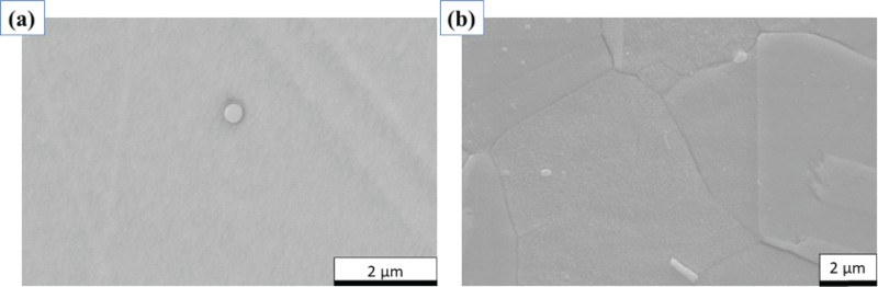
Coarse, equiaxed grains of 36 µm mean grain size were evident in sample A, while the grain structure of sample J was finer (2.4 µm mean grain size) possessing also a minor degree of directionality (see grain structures in Figure 7, calculation of mean grain size based on EBSD results). The grain directionality could be attributed to the precipitated particles distribution at high-angle boundaries, resulting in the elongation of grains in the rolling direction [29]. The average values of grain size of samples A and J showed significant deviation, as it was derived from EBSD and optical microscopy measurements. The stated deviation was anticipated by the different principles and resolution applied for grain size estimation between the two techniques. Unique grain colour maps of samples (a) A and (b) J.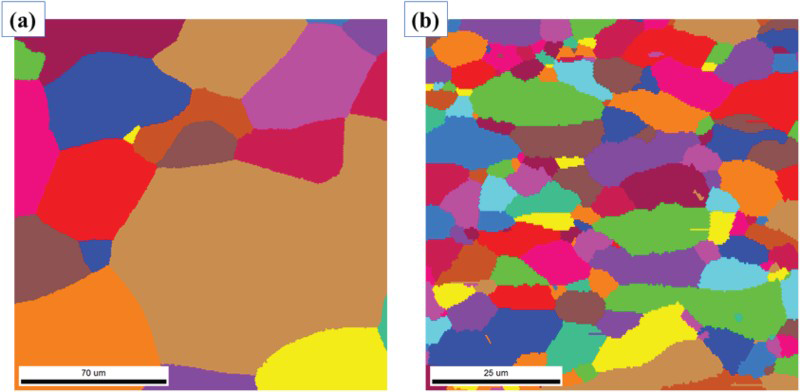
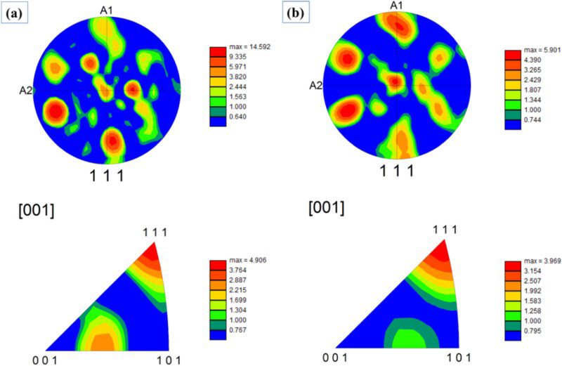
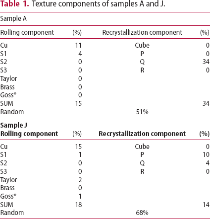
Regarding the texture components analysis, samples A and J exhibited 51% and 68% random texture, respectively (Table 1 and Figure 8). The main difference between these samples lies in the development of recrystallization texture component Q which has been developed in an elevated degree for sample A (34%) which coincides with the whole recrystallization texture percentage. On the contrary, the total percentage of recrystallization texture components in sample J is 14% with only 4% Q component. The rolling texture components percentages were similar for both samples (15 and 18% for A and J, respectively). Examination of IPF texture plots (Figure 9) revealed that preferentially, <111> directions lie normal to the rolled sheet plane followed by <205> and <102> for samples A and J, respectively. Comparison of times-random values showed that sample A exhibited stronger texture than J (4.9 and 4.0 times-random for samples A and J). A similar trend was presented by (111) pole figure texture plots; 14.6 and 5.9 times-random for samples A and J, Figure 9(b). It should be noted that the morphology of pole figure plots could not be correlated to a rolled or annealed standard FCC texture, i.e. Copper or Cube textures.
Inverse pole figure maps of samples (a) A and (b) J. Pole figure (PF) diagrams and inverse pole figures (IPF) of samples (a) A and (b) J. Texture components of samples A and J.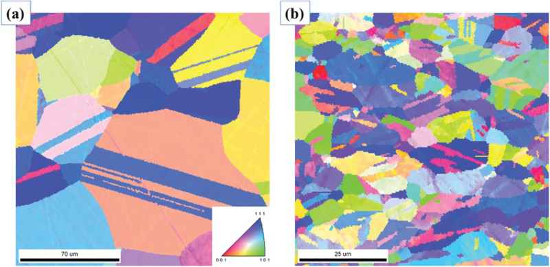
Mechanical properties
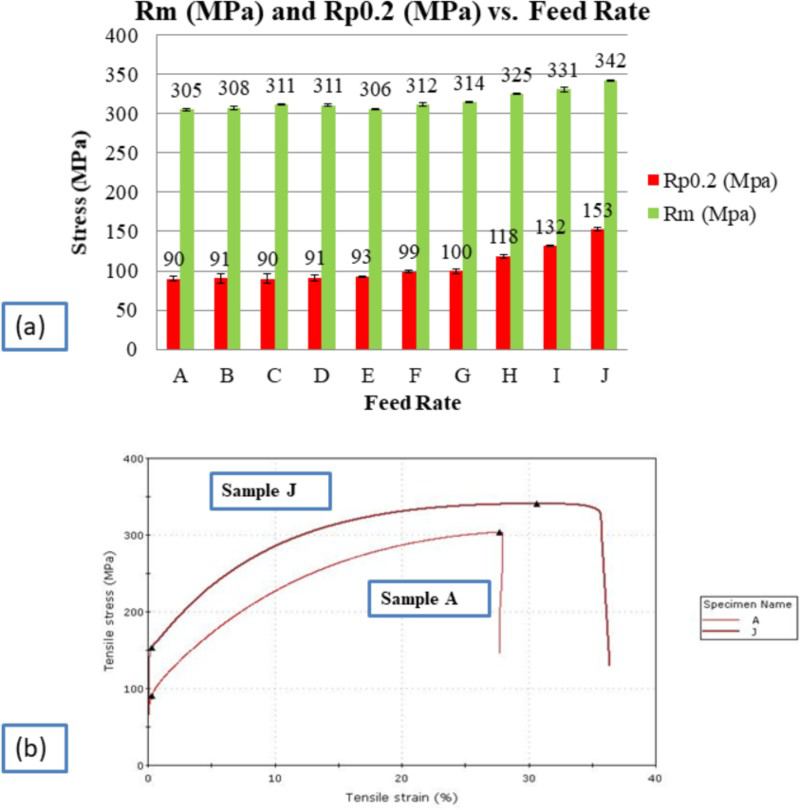
The findings of the tensile properties, bending performance and Vickers hardness are presented (Figures 9). The stress–strain curves for the extreme sample series A and J are presented in Figure 10(b). Ranking of bending folds was conducted using comparative image classification. Summarising the mechanical testing results, a gradual softening tendency is observed, moving from high to low feed rates, i.e. towards greater soaking times, as follows:
Rm: varied from 342 (J-code) to 305 MPa (A-code), ca. 11% reduction (Figure 10)
Rp0.2: from 153 (J-code) to 90 MPa (A-code), ca. 41% reduction (Figure 10)
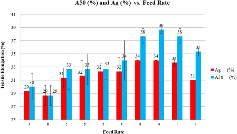
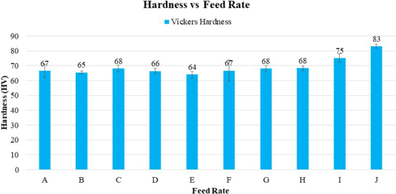
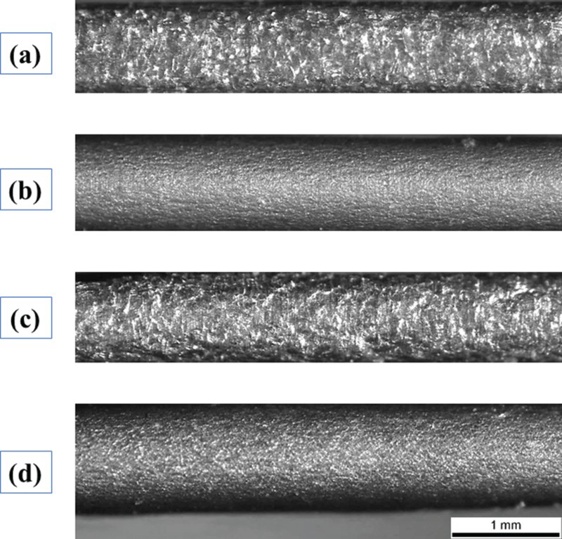
A50: lowering tendency of approximately 17–24% as the feed rate decreases (Figure 11) Vickers Hardness: from 83 HV0.2 (J-code) to 67 HV0.2 (A-code), ca. 19% reduction (Figure 12) Bending performance (at 180° angle) was deteriorated with a decreasing feed rate, which is consistent to the elongation tendency (as it was acquired from the tests performed parallel to the rolling direction), see Figure 13. Sample J exhibited superior properties in bending showing a smooth surface free of defects, such as orange skin, cracks and wrinkles. (a) Evolution of Rm and Rp0.2 (Y-axis) as a function of feed rate (X-axis). (b) Stress–strain curves for samples A and J. Error bars correspond to ±1 s (standard deviation). Evolution of uniform plastic deformation Ag and total elongation at fracture A50 (Y-axis) as a function of feed rate (X-axis). Error bars correspond to ±1 s (standard deviation). Evolution of Hardness (Y-axis) as a function of feed rate (X-axis). Error bars correspond to ±1 s (standard deviation). Bending folds morphology under 180° bending. (a) Sample A (Transverse); orange peel-no cracks, (b) Sample A (Longitudinal); orange peel-no cracks, (c) Sample J (Transverse); smooth surface – no cracks, (d) Sample J (Longitudinal); smooth surface – no cracks.
Fractography
Fractographic analysis of tensile fractures for the two ‘extreme cases’ (samples A and J) is presented in Figure 14. Ductile fracture mechanism was identified through the manifestation of a finely dimpled texture in the case of specimen J with a varied distribution of cavities being evident as regards to their depth and size. Though a heterogeneous distribution of dimple size is revealed – coarse dimples surrounded by fine ones (‘necklace’ morphology), signifying the sequential evolution of micro-void coalescence process as the principal damage accumulation mechanism. Concerning sample A, lower fraction of fracture was covered by shear dimples with characteristic directionality and a non-uniform distribution. The dimpled areas were shallow, while the existent cavities were of smaller size (Figure 14). Multiple deformation ridges originated coming from shear fracture process are evident mostly on the fracture surface. These results are consistent to the extent of the respective total fracture (A50) and post necking elongation measured for A and J specimens. SEM Fractographs of sample A (a and b) and sample J (c and d).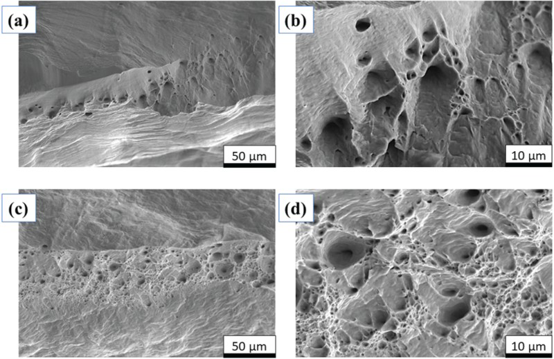
Discussion
Progressive grain size refinement was observed for high feed rates, from A to J as opposed to the electrical conductivity, see Figures 3 and 5. The decreasing tendency in grain size along with the increase in the samples’ electrical conductivity values is attributed to the increasing feed rate, which allows less time for diffusion to take place. High electrical conductivity values (sample J) correspond to a higher density of precipitates due to incomplete solution during soaking. However, it could be anticipated that prolonged solution treatment (sample A), could lead to a more pronounced precipitation during air-cooling, since the driving force for precipitation is greater because of the higher saturation degree, but also to spheroidisation of the precipitates which remain undissolved as a requirement for the minimisation of the systems’ total surface energy. Therefore, it is rather safe to assume that for the current alloy system and conditions, the degree of precipitation, is a more significant factor than grain size in respect to the resultant electrical conductivity values.
There are several factors governing the texture evolution of a recrystallized FCC metal such as grain growth, initial strain and texture, along with the purity of the matrix with respect to alloying elements. More specifically, in the case of Copper and its’ alloys, although the observed recrystallization textures are mainly indicative of a strong cube texture {001}<100>, the existence of alloying elements such as Al, Be, Cd, Mg, Ni, P, Sb, Sn and Zn eliminate the strong cube texture [29]. This is attributed to a distortion of the original deformation texture due to the decrease of the stacking fault energy through the addition of the aforementioned alloying elements. However, although the heat-treated samples contain relatively high amounts of certain aforementioned alloying elements, prolonged solution treatment resulted in grain coarsening, promoting the development of a less random texture with a higher percentage of recrystallization texture components (Q ∼ 34%) in comparison to sample J which exhibited only a 14% total recrystallization texture (Q ∼ 4%) and a 68% random texture (Table 1).
Gradual softening is almost realised as the feed rate is decreased giving rise to higher solution degrees and significant grain coarsening (Figures 10–12). Focusing on the mechanical behaviour of the selected ‘extreme cases’, sample J exhibits higher tensile properties, hardness and bendability in comparison to sample A, which could be adequately explained mainly by the grain size effect and precipitate distribution density. The Rm/Rp (UTS/YS) ratio exhibits an increasing tendency (as feed rate decreases), which is consistent to the higher drop rates followed by yield stress in comparison to the tensile strength giving rise to a higher strain-hardening rate (or work-hardening potential) due to the prolonged solution treatment of the examined CuNiSi strips (Figure 10(a)).
Overall, the better mechanical performance of sample J, in comparison to sample A, is mainly attributed to the finer grain size which is also responsible for better folding/bending properties (Figure 13). The effects of the microstructure on the mechanical properties have a significant impact on the fracture evolution process. Typical fractographic evaluation confirmed the above mechanism for the samples A and J, see Figure 14. The governing ductile fracture process evolves through micro-void coalescence mechanisms. The dimples, mainly created by voids, nucleated around inclusions or intermetallic particles initiated usually in the centre, where the hydrostatic stress is maximum [30]. As the deformation proceeds, the un-fractured material ligaments between the grown voids (behaving as columns or webs) are successively linked to final fracture, forming secondary dimples and leading to a non-uniform distribution of cavities. In between voids, localised shear bands, usually appear. The dimples’ size variation also depends on the void threshold stress and their growth rate, which are predominantly influenced by the microstructural characteristics (e.g. shape, size and nature of second-phase particles, grain boundaries etc.) and their deformation behaviour [31]. The smaller size, depth and density of dimples in sample A compared to sample J, is suggestive of the lower deformation capacity, i.e. strain energy absorbed to fracture, which is mainly connected to the post-fracture elongation (Figure 14). The presence of multiple ‘shear-steps’ and ‘tear-like ridges’ found in sample A is also consistent to diverse deformation mechanism activated, facilitating the evolution of fracture process. Therefore, the drop in the entire ductility of Sample A, which is verified by the fractographic evaluation is mostly related to abnormal grain size, considering also the grain size per strip thickness ratio (63 µm corresponds to ∼16% of the total sample thickness).
Conclusions
Through the present research a correlation between the solution treatment (ST) soaking time of a Cu–Ni–Si alloy and the resulting microstructure, texture, mechanical properties and fracture mechanism, was attempted. The main findings could be summarised below: Lower ST time (higher feed rate) resulted in a fine-recrystallized equiaxed grain structure, exhibiting higher precipitate distribution density of diverse shape and size and, therefore, higher electrical conductivity values. Solution heat-treated Cu–Ni–Si rolled sheets exhibited high amount of random texture while grain coarsening during heat treatment, is associated with an alteration of the resulting texture towards a more oriented microstructure. The degree of solution treatment contributes more to the electrical conductivity than a coarse-grained microstructure for this alloy system. Therefore, electrical conductivity measurements could constitute a reliable quality control procedure to monitor microstructure evolution. Regarding the mechanical behaviour, a low ST time (high feed rate) would result in a sample exhibiting higher tensile properties and better bending performance which could be attributed mainly to the grain size effect and to the different intermetallic particle distribution density. A ductile fracture mechanism was identified in both sample A and J. However, the high ST time (lower feed rate) sample A exhibits a lower dimples’ size and distribution density, and intense shear steps/tear-like ridges, mainly owing to a coarser grain size, leading to lowering the plastic behaviour beyond the onset of localised necking, facilitating, therefore, the fracture process evolution.
Further research
Characterisation of the intermetallic phase particles (coherent–incoherent) existent in the microstructure by extensive TEM analysis is of vital importance for the design of the manufacturing process parameters. This study will shed profuse light to the submicroscopic features of the microstructure, contributing to the achievement of complete solution of the desired phases during solution treatment. Subsequent aging treatments, are also planned as a near-future research project, to provide valuable knowledge regarding the microstructural evolution of the precipitation hardening process, assisting the improvement of the final Cu–Ni–Si product properties.
Footnotes
Disclosure statement
No potential conflict of interest was reported by the authors.