
Abstract
In this work, nanoindentation on a (110) crystal plane with a spherical indenter and (111) twin boundaries at different distances was simulated using molecular dynamics. In addition, the load–displacement curves and mechanical properties were calculated, and the deformation mechanism of the nickel matrix was analysed using a dislocation extraction algorithm (DXA). The results showed that the load decreased in the load–displacement curve, which was caused by the initial nucleation of the dislocations, and the twinning boundary hindered dislocation propagation. Furthermore, Young's modulus values near the twin boundary were lower than those farther away, and the maximum shear stress near the twin boundary was lower. Therefore, dislocation activity in the nickel matrix during indentation was mainly in the form of Shockley partial dislocations.
Introduction
Nickel is an important strategic metal with a wide range of applications in both everyday life and industrial production. Because of its magnetic properties, excellent plasticity, and corrosion resistance, nickel is commonly used in steel, nickel-based alloys and in various military manufacturing equipment such as aircraft and radar. In addition, nickel retains its good mechanical properties at higher temperatures, which makes it a critical component in aircraft engine blades.
As engineering and technology rapidly progress, traditional nickel metals no longer meet the requirements for various applications, and new advancements are needed to strengthen the material. Nanotwinning is a novel way to strengthen a material and has gained the attention of the research community. Structure modification by nanotwinning offers high strength, strong corrosion resistance and high ductility [1-3]. The introduction of nanotwinned structures in nickel allows the material to maintain good plasticity during processing and can greatly improve its mechanical properties. However, because nanostructure materials are difficult to prepare, traditional experimentation is also limited. As a result, molecular dynamics (MD) simulations offer an effective and useful tool to predict the mechanical properties of nanostructured materials at the atomic level, and MD simulations have been widely used for simulating tensile [4-6], compression [5-8] and nanoindentation [9-13] loads. Much effort has been made to investigate the effect of twin boundaries(TB) on the mechanical properties of materials such as Cu and diamond lattice structure, and the corresponding deformation mechanisms. Tucker et al. [5] investigated the role of twin boundaries on copper deformation under tension or compression using MD simulations. The results showed that twinning in copper affected the synergistic effect of the basic deformation mechanisms. Huang et al. [14] also used MD simulations to show that twin boundaries can act as both hardeners and softeners during the nanoindentation of nanotwinned diamond films. Voyiadjis et al. [15] reported MD simulations of nanoindentation of nickel thin films using different indenter geometries of square prismatic, cylindrical and conical indenter. Kum [16] simulated single-crystal nickel to analyse dislocation nucleation and surface elastoplastic deformation in different orientations during nanoindentation. Moreover, Voyiadjis and Yaghoobi [17] investigated the effects of various symmetric and asymmetric tilted grain boundaries(GB) on FCC nickel response during nanoindentation simulation. Talaei et al. [18] investigated the effects of Σ5 grain boundaries on bicrystalline Fe nanoindentation, and Zhang et al. [19] incorporated the atomistic simulation to investigate the response of symmetric and asymmetric P5 GBs during uniaxial tension experiment. They studied the effect of inclination angles on the mechanical response of copper bicrystal In addition, Yaghoobi and Voyiadjis [20] investigated the origin of size effects in nanocrystalline single-crystal nickel films during nanoindentation using large-scale atomic simulations. In summary, research on Ni nanomaterials has focused mainly on GB and single crystal studies, however, less progress has been made in studying the effects of TB on the mechanical properties of Ni materials and the corresponding deformation mechanisms.
Inspired by the above studies, we will investigate the effect of TB on the mechanical properties and deformation mechanisms of nanotwinned Ni under nanoindentation, and explore the corresponding mechanisms in this work using MD simulations. In this study, we used MD simulations to model a spherical indenter on a (110) crystal plane at different positions from the twin boundary of Σ3(111), and we calculated and simulated the nanoindentation process at different distances from the twin boundary. We then studied the evolution of nickel dislocations at different locations from the twin boundary during nanoindentation, and analysed the influence of twin boundaries on the nanoindentation hardness, shear and Young's modulus properties of nickel.
Simulation details and methodology
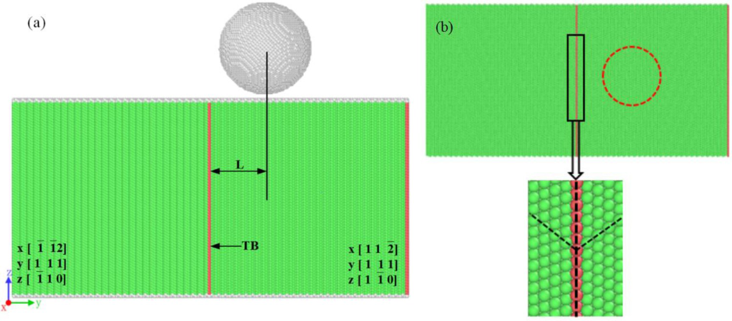
Open-source large-scale atomic/molecular massively parallel simulation (LAMMPS) [21] software was used to perform simulated nanoindentation. and the post-processing software OVITO [22] was used to visualise the atomic structures. The Dislocation Extraction Algorithm (DXA) [23] was employed to identify the dislocations from the atomic configurations [24]. Common neighbor analysis (CNA) [24] is used to distinguish the atomic features. The nickel nanoindentation model under a (110) crystal plane is shown in Figure 1. The distance from the centre of the indenter to the twin boundary was denoted by L, with distances of 0, 30, 50, and 70 Å, and TB represented the Σ3(111) twin boundaries. The dimensions of the nickel substrate were 41a0 × 29a0 × 71a0, where a0 = 0.352 nm was the lattice constant of nickel, and the crystal orientations of the left substrate were [ Twin-crystal Ni nanoindentation model: (a) front view and (b) top view. 2], [111] and [
 10], and the right substrate was [11
 ], [111] and [1
 0] for the right matrix. In this simulation, the indentation of (110) crystalline surface was simulated separately. We placed a spherical diamond indenter with a radius of 40 Å above the substrate, and because diamond is much harder than nickel, it was treated as a rigid body. The spherical indenter was located 5 Å from the upper surface of the substrate, to ensure that the Ni atomic relaxation process was not affected by C atomic compression, to facilitate complete relaxation of the substrate until it reached equilibrium. During the simulations, the substrate atoms were divided from top to bottom into Newtonian, thermostatic and fixed layers. The atoms in the Newtonian and thermostatic layers followed Newton's law of motion, and to reduce the size effect caused by the smaller number of particles than a real system, the model was set to periodic boundary conditions in the X and Y directions. In addition, the upper surface in the Z direction was set to free boundary conditions, and the atoms in the bottom layers of the substrate were fixed to prevent substrate movement.
Furthermore, the model used a hybrid potential function. The EAM (embedded atom method) potential function was used between the Ni–Ni atoms [25], and the specific expression of the EAM was given by:
 represents the potential interaction, F denotes the embedding energy, ρ is the atomic electron density, and i and j denote the elements of two different atoms.
For the interactions between the C–C atoms in the indenter, interactions between the C atoms in the indenter were neglected since the indenter was considered as a rigid body, while the interactions between the Ni atoms in the matrix and C atoms in the indenter followed the Morse potential function [26], as expressed by the following equation:
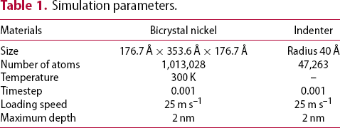
Simulation parameters.
Result and discussion
Dislocation evolution analysis
A load–depth curve was obtained by simulating the depth of the indenter and the sum of the forces applied to the indenter in the z-axis direction. The mechanical properties of the material, such as the modulus of elasticity and hardness, were obtained and further analysed by the load–depth curve. Figure 2 shows the Indentation load–depth curve for single-crystal nickel and the indenter at different distances from the twin boundary. As shown in the figure, the load force was greater than zero when the indenter had not yet entered the matrix, which was caused by repulsion when the distance between the indenter atoms and the matrix atoms was less than the equilibrium distance.
(a) The indentation load–depth curve of indenter at different distances from twin boundary and (b) a locally magnified image of the Red Ellipse.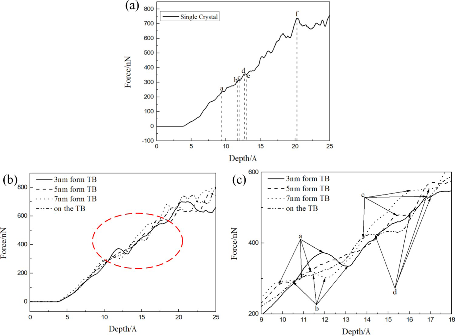
Figure 2(a) shows the load–depth curve of single-crystal Ni, where the load–indentation depth curve was the single-crystal state, and the depth at point a was 9.4 Å. The Indentation load–depth curve for single-crystal Ni increased almost linearly until point a, where the force decreased slightly due to the start of dislocation nucleation. After point a, the indentation force increased almost linearly without significant fluctuations until point b, at which point the indentation depth was 11.7 Å. Between points b and c (12.0 Å), there was a small decrease in load, which was possibly due to the formation and expansion of dislocation loops during this period. When the indentation depth reached 12.7 Å at point d, some new dislocations nucleated under the indenter, leading to a decrease in the indentation force from points d to e. When the indentation depth reached 13.0 Å (point e), the indentation force increased with many small fluctuations. Then, when the indentation depth was 20.3 Å, for example, at point f, numerous dislocations were generated in the single-crystal Ni.
Figure 2(b) shows the load-pressure depth curves when the indenter was located 30, 50, 70, and 0 Å from the twin boundary. The red ellipse is shown in detail in Figure 2(c), and the load–displacement curve for these four scenarios was roughly divided into five stages. Thus we conducted a detailed analysis for this condition, when L = 50 Å.
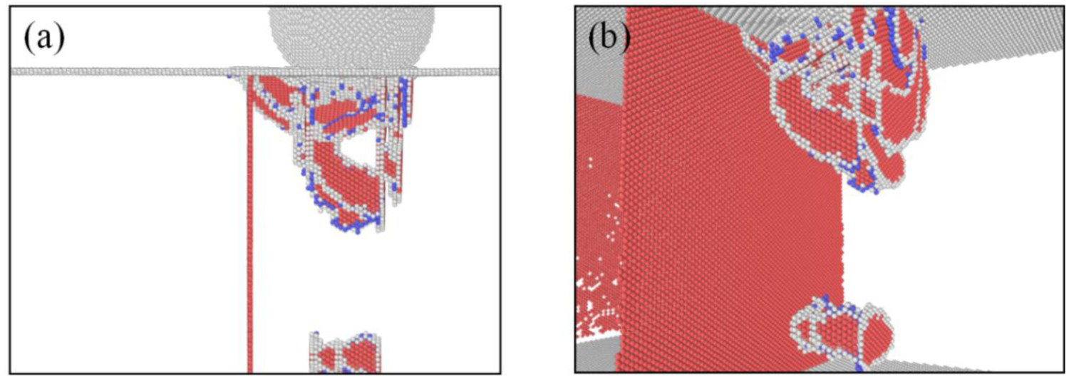
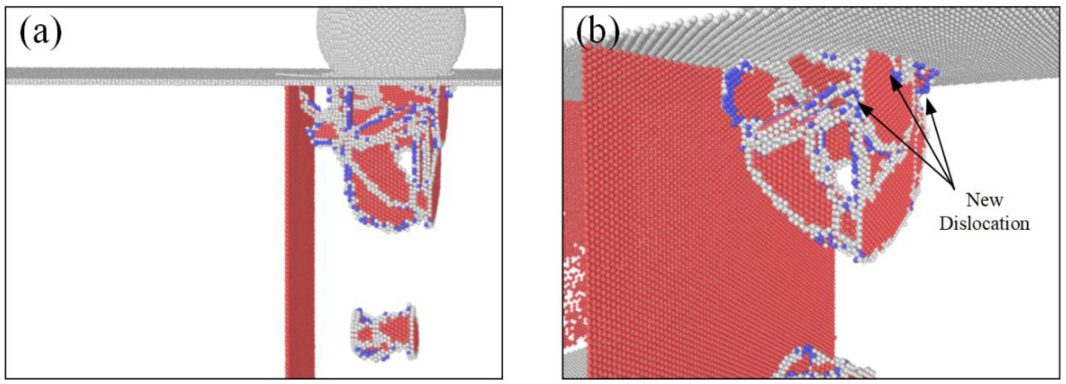
The load–displacement curves are shown in Figure 2(b) and (c), showing phase 1 (from 0 to a). This stage was the elastic behavior stage when shear force reached its maximum at point a. Phase 2 was from a to b, where the first load drop occurred at point b. This was due to the nucleation of dislocations in this stage, and the transition from pure elastic deformation to elastoplastic deformation, and Figure 3(a) and (b) shows the internal dislocations at L = 50 Å before and after the load drop, respectively. In phase 3 (from points b to c), the changes were similar to the behavior during material process hardening, and in this phase, we also observed additional load drop and force fluctuations, which were related to the dislocations generated in the second stage, where some dislocations underwent secondary nucleation. Figure 3(c) shows the end of stage 3, where the dislocations reached the grain boundaries. In phase 4 (points c to d), at point c the dislocations reached the twin boundary and tried to pass the twin boundary. Afterward, when the dislocations merged into the twin boundary, they did not generate any new dislocations in the neighbouring crystals, and the load dropped again at point d, as shown in Figure 4. Phase 5 (from point d onward) had frequent drops and fluctuations in load, and at point d, the dislocations were blocked and new dislocations developed from the initial indentation position, similar to phase 2. The same process was repeated inside the nickel substrate from point d until the end of phase 5, as shown in Figure 5. By analysing the condition when the indenter was located 50 Å from the twin boundary, we found that the four curves had approximately the same form and the remaining three conditions exhibited the same pattern as when the indenter was 50 Å from the twin boundary.
Twinned nickel indentation process diagram (L = 50 Å) (a) before the load drops: elastic deformation occurs, (b) after the load drops: the dislocation volume suddenly increases, (c) at the end of the third stage, the dislocation reaches the grain boundary and merges to the grain boundary. Simulation at point d, dislocations have reached the grain boundary and coalesced into the grain boundary plane, no new dislocations have been created in the adjacent crystals (a) looking straight ahead and (b) in the top view. New loads are generated at the head position (a) forward view and (b) elevation view (the arrows refer to the generation of new dislocations).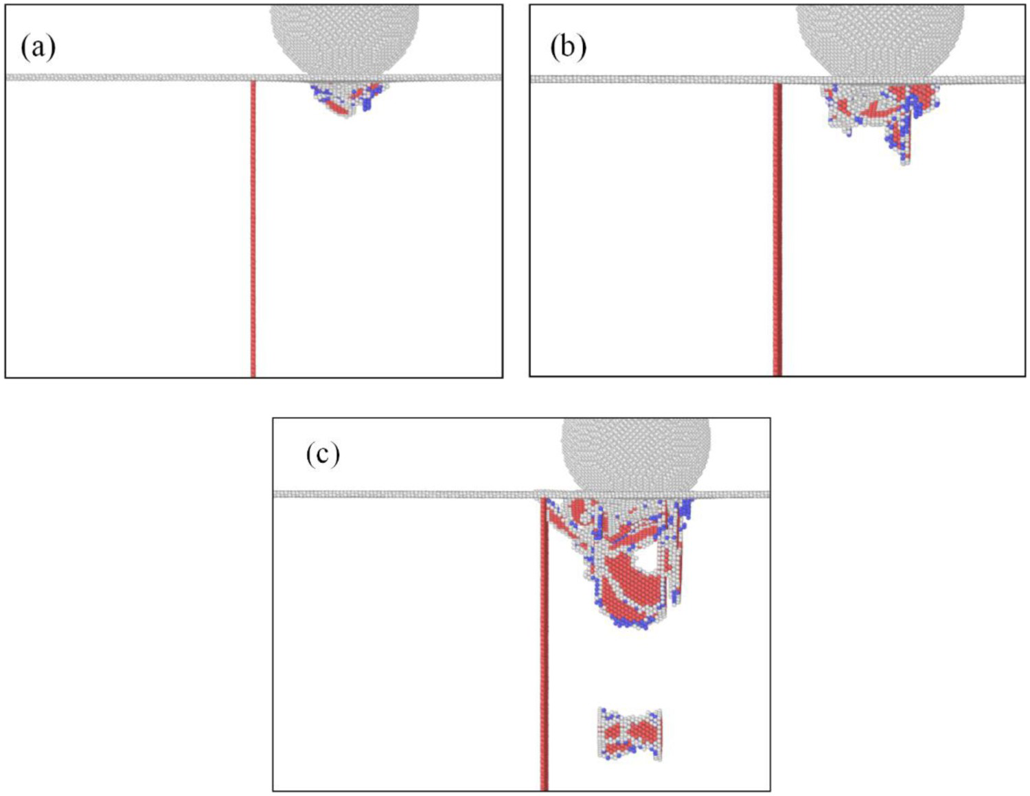
By comparing the load-displacement curves for Ni in the single-crystal state and the state containing twin boundaries, we found that these curves were roughly consistent with each other during the pre-indentation period, and they all increased almost linearly. This indicated that single-crystal Ni and Ni contained twin boundaries that experienced the same nanoindentation deformation mechanism during the pre-indentation period. However, the first load drop occurred in the single-crystal Ni curve when the indentation depth was 9.4 Å. In these four conditions with twin boundaries, the first load drop occurred when L = 0 Å and the indentation depth was 11 Å. When L = 30 Å, the first load drop occurred at an indentation depth of 11.8 Å. When L = 50 Å, the indentation depth was 10 Å, and the load drop occurred at an indentation depth of 11.2 Å when L = 70 Å. Therefore, the nickel that contained twin boundaries experienced a load drop point later than the single crystal state material, possibly due to the obstructive effects of the twin boundaries on dislocation expansion during indentation. Moreover, during the middle and late stages of indentation, the obstruction and absorption of dislocations by twin boundaries alternated, and the load decreased when the dislocations were absorbed by the twin boundaries.
Distribution of crystal defects at different depths in Ni nanoindentation simulations with different L.
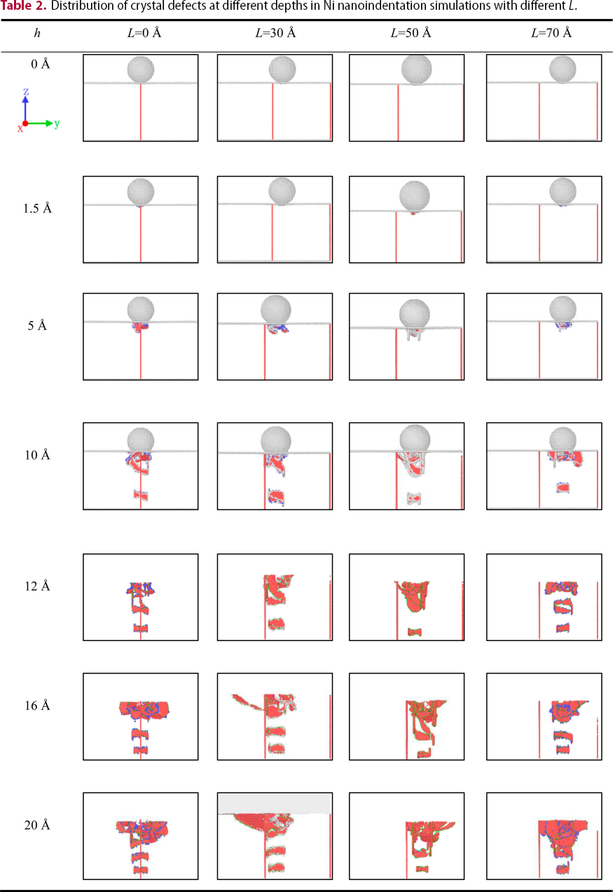

At an indentation depth of 1.5 Å, dislocations had not yet generated inside the nickel matrix at L = 30 Å, and the dislocations started to nucleate and enter the plastic deformation stage. When the indentation depth was 5 Å, the contact surface area between the spherical indenter and the nickel substrate increased, and dislocation reactions around the indentation increased. At an indentation depth of 10 Å, the first dislocation loop formed under the indentation and a second dislocation loop formed as the indenter continued to press down. At an indentation depth of 12 Å, a prismatic dislocation ring formed below the indentation, and the first dislocation loop moved downward for some distance compared to the previous phase. At an indentation depth of 16 Å, a second dislocation loop formed below the indentation, and the maximum indentation depth was reached at 20 Å. Dislocations were generated in the adjacent crystals at indentation depths of 16 and 20 Å, possibly because during the indentation process, the force of the indenter was also applied to the twin grain boundaries, causing dislocation generation at the twin grain boundaries.
At L = 50 Å, the dislocations evolved into Shockley partial dislocations with a Burr's vector of 1/6 <112> at an indentation depth of 1.5 Å. As the indenter continued to press down, the contact area between the indenter and the substrate increased, and the dislocations at the indentation site increased. At an indentation depth of 10 Å, a dislocation ring formed within the substrate, and a Burgers vector in the 1/3 <100> Hirth dislocation and a 1/6 <110> stair-rod dislocation were also present in the dislocation loop. At an indentation depth of 12 Å, we observed that the initially generated dislocation loop shifted down from the previous stage, and at an indentation depth of 16 Å, a prismatic dislocation loop was generated below the indentation. In addition, at an indentation depth of 20 Å, two prismatic dislocation loops were generated below the indentation.
At L = 70 Å, during the first stage of indentation, changes inside the nickel substrate were similar to the remaining three conditions, except for when the indentation depth was 12 Å, and two dislocation loops were generated below the indentation. As the indenter continued to press down, the contact surface area between the spherical indenter and the nickel substrate increased and the reaction around the indentation intensified. At an indentation depth of 20 Å, the second dislocation loop was absorbed by the dislocations below the indenter.
The analysis of the evolution of internal dislocations shows that, the force drop in the indentation load–depth curve of Figure 2 can also be explained as the formation of 1/6 <112> Shockley partial dislocations and stacking faults. This transfers the external work to strain energy (or formation energy) of dislocations and stacking faults. On the contrary, 1/6 <112> + 1/6<112> → 1/3 <100>, 1/6<112> + 1/6 <112> →1/6<110> and other kinds of dislocation reactions release strain energy. The release of strain energy is the outcome of one of the two spontaneous dislocation reaction conditions without external force (The other condition demands that Burgers vectors are conserved with a reaction). This leads to the rise of force. Taking together, the indentation load-depth curve shows a fluctuation [10].
The dislocation extraction method [23] consisted of Burgers vectors at different dislocations and at different distances from the twin boundary, and the lengths of their dislocations are shown in Figure 6. The figure shows that with an increase in the indentation depth under the indenter, the overall dislocation length increased. During plastic deformation in the nickel, the number of Shockley dislocations increased, while the number of other dislocations remained stable, thus in the nickel matrix, dislocation nucleation was mainly due to the movement of Shockley partial dislocations. When the indenter reached the twin boundary, the Shockley dislocation lengths reached their maximum at an indentation depth of 18 Å. When the indenter distance was 30 Å from the twin boundary, the length of Shockley dislocation reached their maximum at an indentation depth of 18.75 Å, and when the indenter distance was 50 Å from the twin boundary, the Shockley dislocation lengths reached their maximum at an indentation depth of 20 Å. As shown in Figure 6(d), when the indenter was 70 Å from the twin boundary, the Shockley dislocation length slightly fluctuated during the indentation process, compared to other positions and reached its maximum at the indentation depth.
Dislocation length–indentation depth curve: (a) L = 0 Å, (b) L = 30 Å, (c) L = 50 Å and (d) L = 70 Å.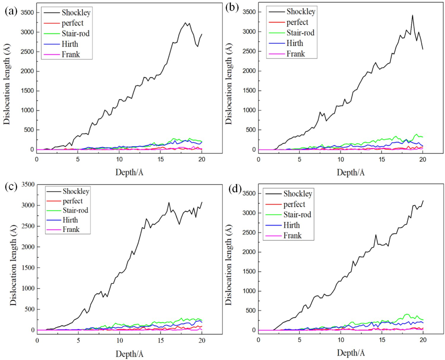
Figure 7 shows the total dislocation, Shockley dislocation and other dislocation lengths during the indentation process. As indentation depth increased, the length of the total dislocation line increased overall, and the lengths of the Shockley and other dislocations, as well as total overall dislocations increased following the same trend, and the curve exhibited a sawtooth shape. As shown in Figure 7, the total length of the Shockley dislocations and the dislocation line almost coincided at an indentation depth of 0–5 Å. When the indenter was located at the twin boundary, the average Shockley dislocation length was 89.1% of the total dislocation length, and when the indenter was 30 Å from the twin boundary, the average Shockley dislocation length was 86.3% of the total dislocation length. When the indenter was located 50 Å from the twin boundary, the average Shockley dislocation length was 87.2% of the total dislocation length. Thus the average Shockley dislocation to total dislocation line length was 87.2% when the indenter was 70 Å from the twin boundary.
Dislocation length–indentation depth curve (total dislocation length in figure, Shockley total dislocation length in indentation, and dislocation length in other dislocations): (a) L = 0 Å, (b) L = 30 Å, (c) L = 50 Å, (d) L = 70 Å.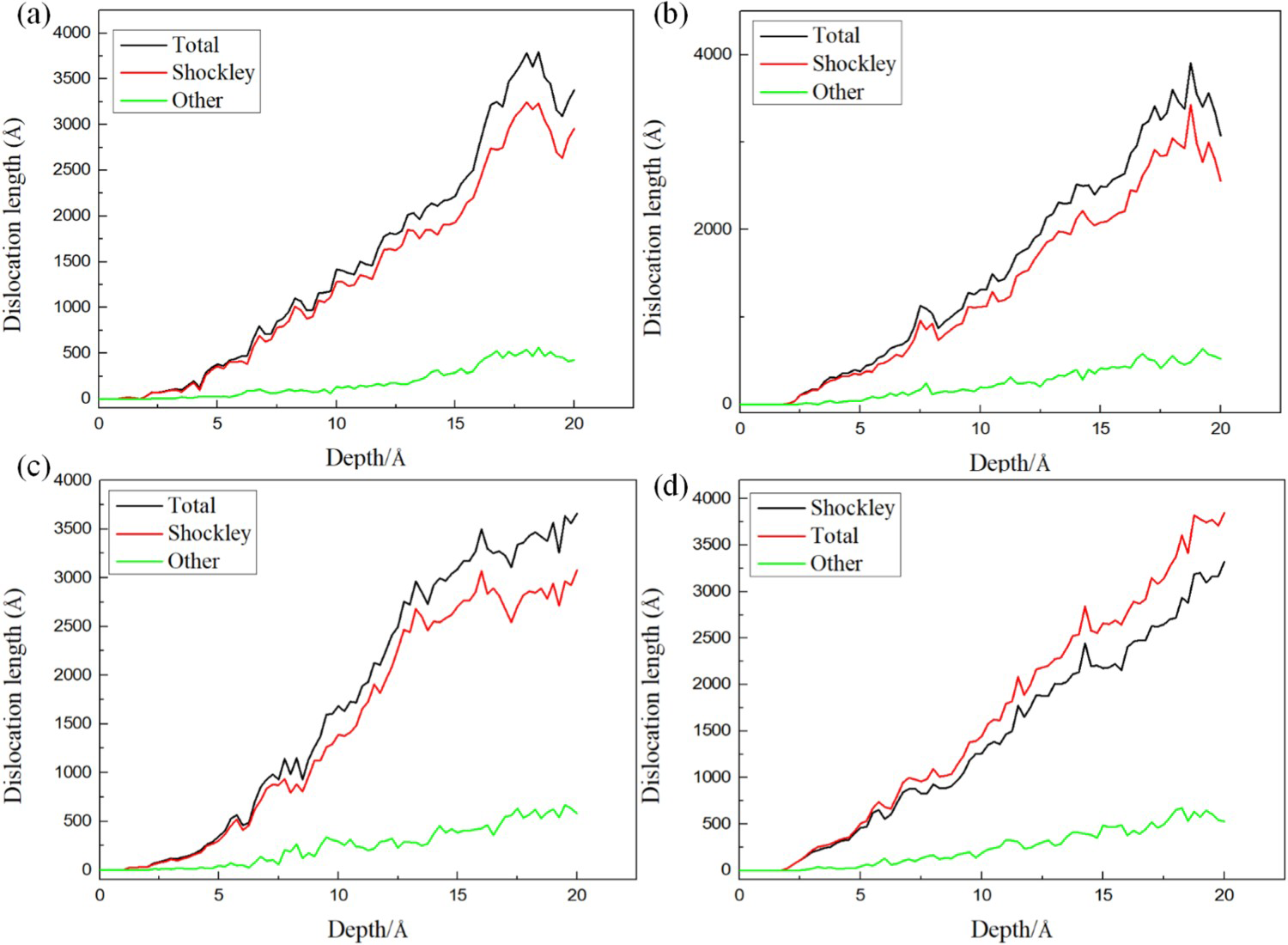
As can be seen from Figure 8, in the nanoindentation process, when the indenter is closer to the twin boundary, the dislocation line length curve is shifted below the other curves, and the total length of the Shockley incomplete dislocations is smaller than that of the dislocations at other indentation locations. The reason is that when the indenter is closer to the twin boundary for nanoindentation, the twin boundary will absorb part of the dislocations, which makes the dislocation activity at the twin boundary and the indenter side decrease significantly, and the activity of incomplete dislocations also decreases, and the dislocation reaction decreases, and all kinds of stacking faults also decrease; in addition, when the indentation location is gradually moved away from the twin boundary, the trend of the dislocation curve is the same, and the influence of the twin boundary on the dislocation evolution of the indentation process decreases in turn, consistent with the situation described of [13].
Nanoindentation process L = 0 Å, L = 30 Å, L = 50 Å, L = 70 Å specimen shockley dislocation length curve.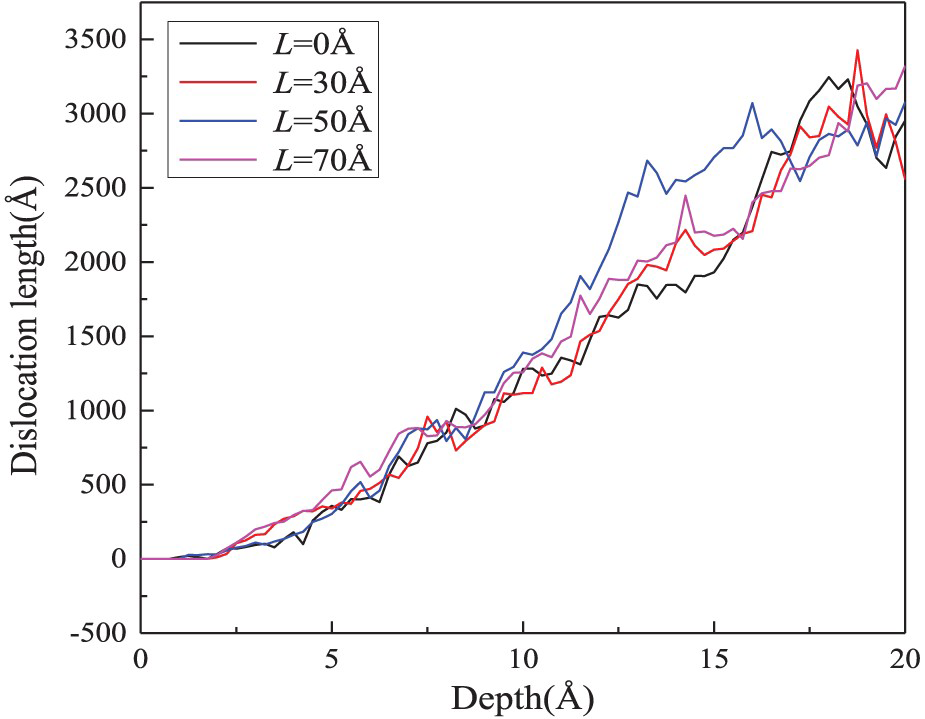
Mechanical property analysis
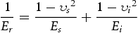
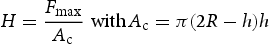
Hertz found that the radius of the contact circle a is related to the indenter load P, with an indenter radius of R, and considering the elastic properties of the contact material, according to equation (3):

calculation parameters at different distances from grain boundary.
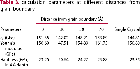
As the distance of the indenter from the twin boundaries increased from 30 to 70 Å, Young's modulus and hardness values increased with increasing distance. When the indenter was located at the twin boundary, the hardness value was greater than the hardness value at L = 30 Å, but was less than the obtained hardness values at L = 50 Å and L = 70 Å. The Young's modulus at L = 0 Å was greater than L = 30 Å and L = 50 Å, but less than L = 70 Å. In addition, Ni in the single crystal state had Young's modulus greater than at L = 30 Å and was also less than at L = 0, 50 and 70 Å. Therefore, the hardness values for single crystal Ni were greater than those at L = 0 and 30 Å, and less than at L = 50 and 70 Å. The larger hardness values obtained farther away from the twin boundary were attributed to the twin boundary, which prevented the dislocations from expanding. The Young's modulus and hardness values that were observed closer to the twin boundary were both smaller than those away from the twin boundary, as during the indentation process, the force of the indenter was also applied to the twin boundary, causing dislocation formation on the twin boundary as well; thus, both Young's modulus and hardness values were smaller than those away from the twin boundary.
Stress–strain variation and distribution
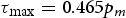
When the maximum shear stress reaches its critical point, homogeneous dislocation nucleation occurs, and the maximum shear stress can be estimated by the elastic contact theory [31]:

Load and maximum shear stress at point a.
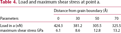
The equivalent stress is defined by von Mises stress (σvon), which is a combination of normal and shear stresses and is determined by
Figure 9 shows the shear strain on the nickel atoms at different distances from the twin grain boundary during indentation, at an indentation depth of 20 Å. All atoms were coloured according to the value of local atomic shear strain, where the blue atoms mean the lowest shear strain, and the red atoms represent the highest shear strain. In the figure, the red atoms represent shear strains greater than or equal to 2, showing that the shear strain applied to the atoms during loading varied slightly with L. The figure also shows that the high shear strain region was mainly concentrated around the indentation region, which was the contact area between the indenter and the substrate. This was attributed to the atoms in the indentation region, which were directly influenced by the pressure generated by the indenter [32].
Atomic shear strain diagram: (a) L = 0 Å, (b) L = 30 Å, (c) L = 50 Å and (d) L = 70 Å.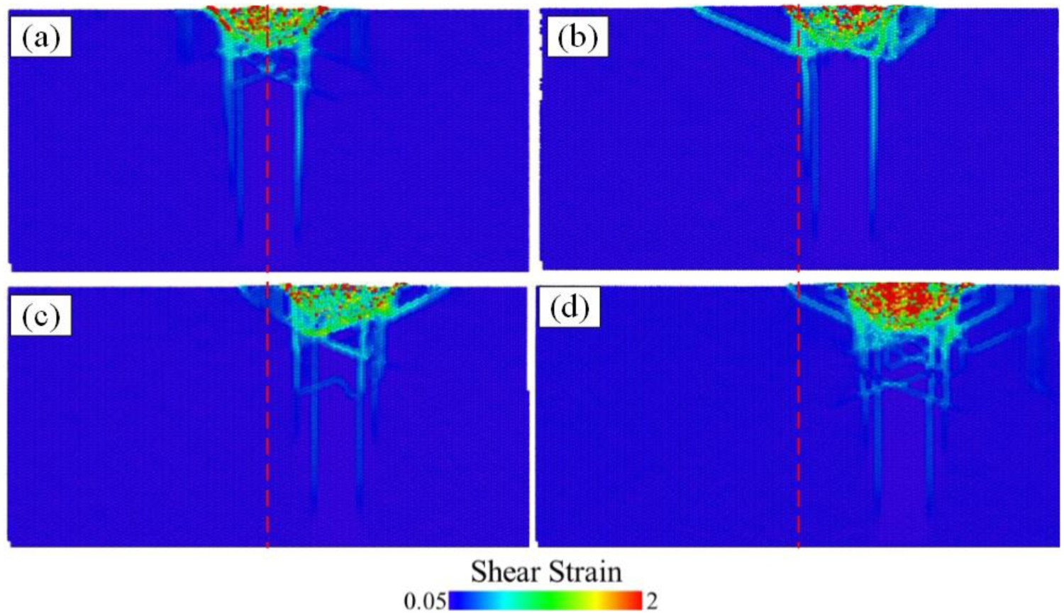
The atomic displacement vector of nickel during the indentation process is shown in Figure 10, where the black arrows point in the direction of atomic motion and the black dashed lines indicate twin grain boundaries. As shown in Figure 10, the atoms moved to form a distinct curve around the indenter, owing to the shear stress flow. As indentation proceeded, the atomic displacement vectors in the indentation region remained relatively symmetrical, indicating isotropic deformation of the nickel during the indentation process. Furthermore, the nickel atoms that were in contact with the indenter moved toward the sides of the indenter.
Atomic displacement vector diagram of the indenter at different indenter positions at 2 nm: (a) L = 0 Å, (b) L = 30 Å, (c) L = 50 Å and (d) L = 70 Å.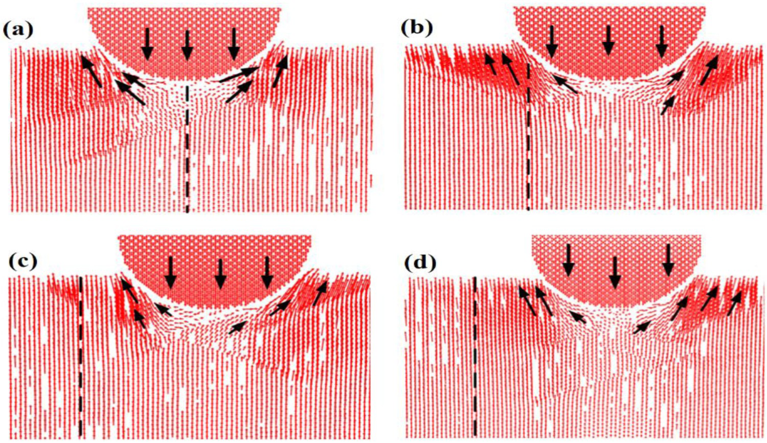
Conclusion
During indentation, the dislocation length and the load–indentation curves showed a certain periodicity, which was related to the dislocation evolution, nucleation, reaction, dislocation loop formation, and dislocation absorption and hindrance of the twin grain boundaries during indentation. The total length of Shockley partial dislocations during the indentation process accounted for more than 80% of the overall dislocation length, and the dislocation reaction in the nickel matrix during the loading process was dominated by the reaction of partial dislocations. The Young's modulus and the hardness of the nickel substrate were significantly affected by the twin boundary, and the closer the distance to the twin boundary, the lower the performance. The indentation hardness and Young's modulus values at 30 Å from the twin boundary were the smallest, at about 20.3 and 148 GPa, respectively, as the twin boundaries effectively blocked dislocation expansion when the indenter was farther away from the twin boundaries (50 and 70 Å). This increased the measured hardness below the indenter. Compared to single-crystal nickel, the properties of the material with twin boundaries were higher compared to the single-crystal state material. The maximum shear stress at the twin grain boundary was lower than the maximum shear stress away from the twin grain boundary. During the indentation process, the nickel atoms moved symmetrically about the indenter, while the nickel atoms in contact with the indenter moved to both sides of the indenter.
Footnotes
Acknowledgements
This research was funded by the S&T Program of Hebei Province (No. 20311003D) and Shanghai Engineering Research Center of Hot Manufacturing, Shanghai Dianji University (18DZ2253400). The numerical calculations in this paper have been done on the supercomputing system in the High-Performance Computing Center of Yanshan University.
Disclosure statement
No potential conflict of interest was reported by the author(s).