
Abstract
The Ni-5 at.%W/Ni-9.3 at.%W/Ni-5 at.%W alloy composite substrate with a thickness of 109 μm was produced by powder metallurgy and rolling process. The composite substrates with different thicknesses were produced by electrochemically polishing the outer layer of each substrate. When the thickness of the composite substrate was reduced to 72 μm, the cubic texture could still reach 97.3% by using electron backscatter diffraction. Moreover, its saturation magnetization only reached 2.3 (emu/g). Finally, the cubic texture of composite substrates was found to vary in thickness thinning because the grain growth mechanism between the inner and outer layers is different. The inner layer defect has a “pin” effect on grain boundary migration, and in the outer layer, the cubic grain grows more easily to the surface and along the rolling direction. However, the formation of cubic-oriented grains is hindered by the twin defects in the inner layer.
Introduction
The high temperature superconductor material REBa2Cu3O7-δ (REBCO) has been widely used in the electric power area [1,2]. Unlike multi-filamentary wires like the low temperature superconductor material NbTi and Nb3Sn, the REBCO commercial tape has a coated conductor structure consisting of the metallic substrate, buffer layer, superconductor layer, Ag cap layer, and Cu stabiliser layer. Although both layers have been deeply investigated [3-7], the metallic substrate to provide mechanical strength is always one of the most important parts. Different application requirements should be achieved in different layers, such as the high current capability in the superconductor layer and the high thermal conductivity in the Cu stabiliser layer. The most important index is the metallic substrate's high mechanical strength and as low magnetisation as possible. Moreover, the thinner but stronger and low-cost metallic substrate is a better choice for large-scale commercial REBCO tape production [8].
Numerous substrate materials can be selected in the preparation process of coated superconducting strips by rolling assisted biaxially textured substrates technology (RABiTS). Among these, the most widely studied is the Ni–W alloy, which is low-cost and capable of easily forming strong cubic textures [9,10]. The substrate made of nickel alloy with 5% tungsten (Ni5W) is the most promising material for industrial production. However, the hysteresis loss of the Ni5W alloy substrate is severe such that its saturation magnetisation reaches as high as 26.1 emu g−1 at 1 T, causing hysteresis loss in alternating current applications [11]. Subsequently, Ni7W and Ni9.3W alloy substrates with high W contents were produced to reduce the hysteresis loss. However, the formation of cubic crystal nuclei in substrates with high W contents is not facile, resulting in lower cubic texture contents. This situation changed when Ni–W composite alloy substrates with a tri-layer structure emerged. Remarkably, the Ni5W/Ni9.3W/Ni5W (Ni-5 at.-%W/Ni-9.3 at.-%W/Ni-5 at.-%W) alloy composite substrate not only forms a strong cubic texture but also achieves high yield strength, which is more suitable for preparing coated superconducting strips. However, severe hysteresis loss persists under the coated superconductor's operating conditions (77 K, 3 T) [12-14]. Hence, it is a good attempt to reduce the overall magnetisation by thinning the outer thickness of the Ni5W/Ni9.3W/Ni5W/composite alloy substrate. When the composite substrate thickness of a sandwich structure is overly large [15,16], the cross-sectional area of the coated superconducting strip increases. This reduces the critical current density of engineering [17] and increases the overall weight of the superconducting strip, further limiting the strip's engineering application. Evidently, it is of great significance to reduce the thickness of the NiW alloy composite substrate. Moreover, the investigation of changes in the magnetisation and recrystallisation mechanism of strong cubic texture after reducing the thickness of the Ni–W alloy composite substrate is anticipated to advance the practical processing of coated superconductors.
The Ni5W/Ni9.3W/Ni5W alloy composite substrate is the research object in this study. To reduce its thickness, the electrochemical polishing method is employed. Furthermore, the formation mechanism of the cubic texture of the composite substrate with different thicknesses is investigated and the magnetisation of the composite substrate with different thickness are explored. Finally, the thin Ni–W alloy composite substrate suitable for preparing coated superconducting strips is fabricated. In addition, the Ni8W/Ni12W/Ni8W composite substrate is employed for simple verification.
Experiment
Alloys composed of Ni5W and Ni9.3W using nickel (99.9%) and tungsten (99.95%) powders were mixed for 5 h under the protective atmosphere of Ar-4% H2 in a high-energy planetary ball mill. The mixed powders of Ni9.3W and Ni5W were loaded into a graphite mould from bottom to top in order and cold-pressed at 15 MPa of axial pressure. Then, a 7-mm-thick composite alloy ingot was sintered at 850 °C under 20 MPa pressure by spark plasma sintering. The ratio of the Ni5W/Ni9.3W/Ni5W composite ingot was fixed at 1:2:1. The ingot was homogenised under 1100 °C under an Ar-4% H2 atmosphere for 24 h. The composite ingot was cold-rolled to a thickness of 109 µm at a 5% reduction rate. The Ni5W/Ni9.3W/Ni5W composite substrates were thinned by the electrochemical polishing method to produce composite substrates with different thicknesses. An environment-friendly, chromium-free polishing solution H3PO4–H2SO4 was used [18]. The composite substrate and nickel plate were used as the anode and cathode during the polishing process. The polishing solution was placed in a water bath at 45 °C and stirred continuously. After different polishing times, Ni5W/Ni9.3W/Ni5W composite substrates of varying thicknesses were obtained. Then, all substrates were recrystallised at 750 °C for 1 h and 1250 °C for 2 h in an Ar-4%H2 atmosphere. To confirm the feasibility of the polished method for increasing the W content in the composite substrate, the Ni8W/Ni12W/Ni8W composite substrate is also tested. The detailed fabrication process of the Ni8W/Ni12W/Ni8W sample was reported in our previous literature [10]. In brief, the 1:2:1 ingot was rolled to 103 µm, and four intermediate annealing steps were introduced during the cold-rolling process at different thicknesses. After different polishing, the Ni8W/Ni12W/Ni8W samples were recrystallised by the two-step annealing process with the first step at 700 °C/1 h and the second step at 1350 °C//2 h.
Furthermore, the texture of composite substrates was characterised by scanning electron microscopy (SEM, QUANTA FEG 450) equipped with a backscattered electrons detector (EBSD, EDAX). The data obtained were evaluated by OIM software developed by TSL. The EBSD results, the S orientation 123〈634〉, copper 112〈111〉, Brass 011〈211〉, Goss 011〈100〉 and cube 001〈100〉 were defined in the tolerance angle of 15°, and the orientation fractions were obtained by the OIM software. The low-angle boundaries (LAGB) and high-angle boundaries (HAGB) were defined as boundaries with misorientations of 2–15° and >15°. The Σ3 boundaries were defined by applying a maximum deviation of 3° from the ideal 60 〈111〉 misorientation. The backscatter electron image (BSE) is used to detect the sample to focus on the elementary concentration in a different part of the sample. The magnetisation was measured by PPMS from Quantum Design. The surface roughness is measured by atomic force microscopy (Bruker Dimension icon with ScanAsyst) and the RMS (root mean square) value is used to reflect the roughness.
Results and discussion
The BSE of the RD-ND (rolling direction–normal direction) cross section of Ni5W/Ni9.3W/Ni5W composite substrates with different thicknesses are shown in Figure 1. Overall, these composite substrates obtained by electrochemical polishing have no distinct interface traces between the surface and inner layers. The thickness of the whole tape is measured and the thicknesses are 100.5 ± 0.6, 93.4 ± 0.7, 89.9 ± 2.7, 72.1 ± 2.9 , 63.9 ± 0.6, and 52.3 ± 0.3 µm, respectively, which proves that we can effectively decrease the thickness of the composite substrate by electrochemical polishing. Otherwise, the Ni8W/Ni12W/Ni8W composite substrate used in this experiment is the same as the Ni5W/Ni9.3W/Ni5W composite substrate obtained by powder metallurgy sintering used for composite alloy ingots. The same cold-rolling process as Ni5W/Ni9.3W/Ni5W was applied to produce a 103.2 µm-thick Ni8W/Ni12W/Ni8W composite substrate. With the same electrochemical polishing parameters, we obtained Ni8W/Ni12W/Ni8W composite substrates with thicknesses of 85.2 ± 0.1, 75.5 ± 0.2, and 66.4 ± 0.3 µm, respectively. For convenience, in the following text, all the samples are named using the integer bit of the thickness. For example, the 100.5 ± 0.6 µm sample will be called 100 µm.
The BSE images of RD-ND cross section of Ni5W/Ni9.3W/Ni5W composite substrates with different thicknesses after recrystallisation annealing: (a) 100, (b) 93, (c) 89, (d) 72, (e) 63, and (f)52 µm.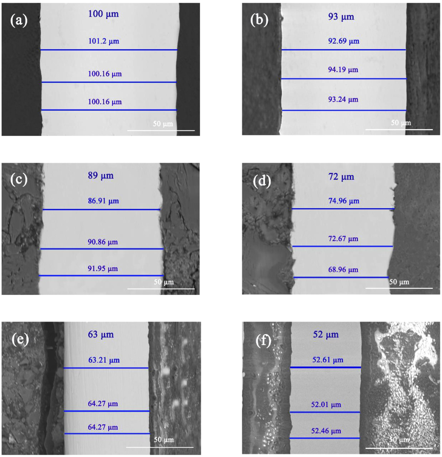
Ni5w/Ni9.3W/Ni5W composite substrate
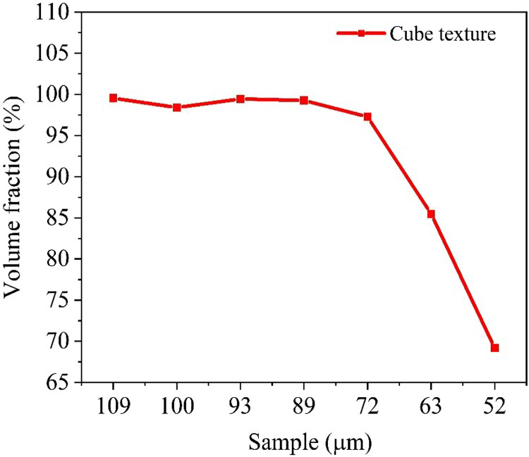
The atoms on the surface layer and inner layers of the Ni5W/Ni9.3W/Ni5W composite substrate diffuse into each other during heat treatment, which is closely related to the formation of the final cubic texture. To study the cubic texture evolution of composite substrates on the surface with different thicknesses after gradual polishing and thinning, a two-step recrystallisation heat treatment was carried out on seven unpolished and polished composite substrates with different thicknesses. Then, the EBSD test was performed on the RD-TD (rolling direction–transverse direction) surface of the composite substrates to achieve a strong cubic texture on the surface of the thin composite substrate. Figure 2 shows the inverse pole figure (IPF) on the RD-TD surface of Ni5W/Ni9.3W/Ni5W composite substrates with different thicknesses after recrystallisation annealing. The figure legend denotes that the grain has a cubic orientation. The closer the grain colour is to red, the nearer the orientation to the cubic orientation; the converse is also true. As shown in Figure 2(a–d), when the thicknesses of the Ni5W/Ni9.3W/Ni5W composite substrates are 109, 100, 93, and 89 µm, the RD-TD surface forms a relatively sharp cubic texture. Figure 3 indicates that the cubic texture contents are 99.4%, 98.3%, 99.3%, and 99.2%, respectively. When the thickness is reduced to 72 µm after polishing, some obvious non-cubic-oriented grains appear on the surface (Figure 2(e)). However, the non-cubic-oriented grain content is extremely small such that the cubic texture content still reaches 97.3%. When the thickness is reduced to 63 µm, more grains deviating from the cubic orientation appear on the RD-TD surface; the cubic texture content decreases obviously to 85.6%. In view of this, the 52 µm-thick composite substrate further thins. The RD-TD surface contains numerous non-cubic grains and the cubic texture content is only 69.2%. The statistics in Figure 3 indicate that before the composite substrate is reduced to 72 µm by polishing, the cubic texture content (which exceeds 97%) on the surface slightly fluctuates. When the thickness drops to 63 µm, the cubic texture content decreases, following a cliff-like pattern.
EBSD maps of RD-TD surface of Ni5W/Ni9.3W/Ni5W composite substrates with different thicknesses after recrystallization annealing (a) 100, (b) 93, (c) 89, (d) 72, (e) 63, and (f) 52 µm. Statistical graph of cubic texture content on the RD-TD surface of Ni5W/Ni9.3W/Ni5W composite substrates with different thicknesses.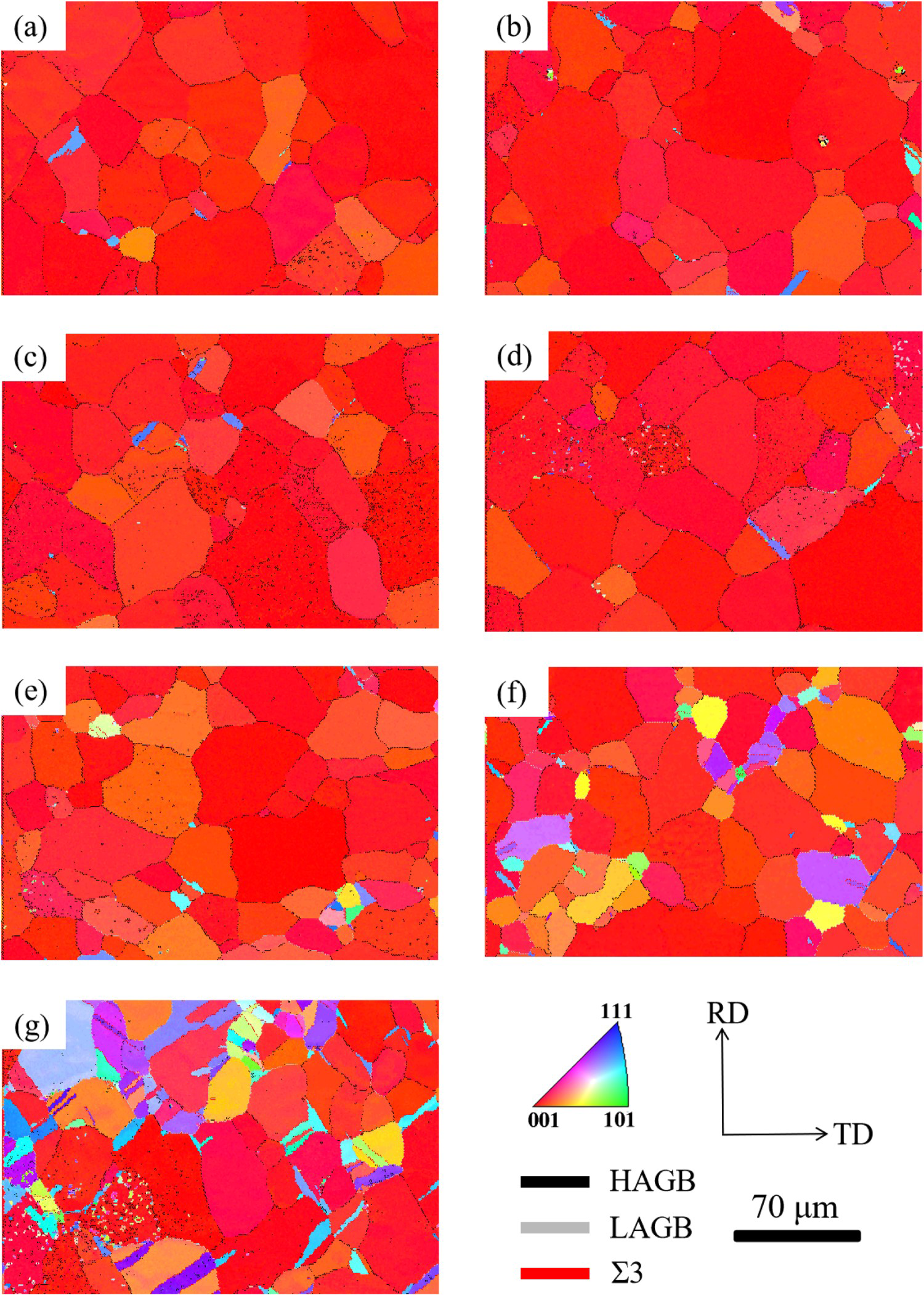
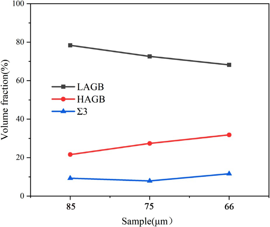
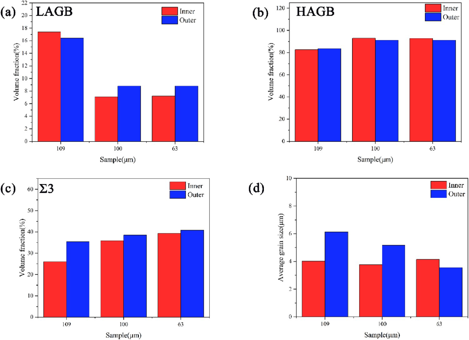
As shown in Figure 4, the HAGB, LAGB, 2−15°, and Σ3 twin boundary contents on the surface of the Ni5W/Ni9.3W/Ni5W composite substrates with different thicknesses are found after statistics. With a decrease in the thickness, all the grain boundary contents only have a slight fluctuation. However, when the thickness reaches 72 µm, the LAGB content sharply decreases, and the HAGB and Σ3 twin boundary contents increase. Such variability of the grain boundary fractions coincides with the change of the cube texture, as shown in Figure 3. It indicates that the HAGB is along with the non-cube orientation grains. The origination of such a phenomenon will be discussed later.
Volume fractions of LAGB, HAGB and Σ3 boundary of Ni5W/ Ni9.3W/Ni5W composite substrates with different thicknesses after recrystallisation annealing.
To investigate the synergistic change in the outer and inner layers of the Ni5W/ Ni9.3W/ Ni5W composite substrates, the EBSD tests for the RD-ND cross section of these substrates were examined. Figure 5 shows the EBSD orientation distribution for the entire RD-ND cross section of the Ni5W/Ni9.3W/Ni5W composite substrates with different thicknesses after a two-step recrystallisation heat treatment. The figure indicates that in the thinning process of electrochemical polishing, the thinned area is the outer layer of the composite substrate. Accordingly, Figure 5 clearly indicates the division between the outer and inner layers. The unpolished 109 µm-thick outer layer of the composite substrate is full of cubic-oriented grains. Moreover, the cubic-oriented grains in the outer layer tend to grow towards the inner layer. Consequently, the inner layer also contains a small quantity of cubic-oriented grains. However, a few grains with non-cubic orientations also exist at the junction of the inner and outer layers. This results in the final transformation of the cubic grains of the outer layer into non-cubic-oriented grains. The EBSD orientation distribution maps of the composite substrates with thicknesses of 89, 72, and 63 µm show that some non-cubic-oriented grains appear at the interface between the inner and outer layers. This indicates that the non-cubic orientation of the outer layer grains at the interface with the inner layer is due to the erosion of the non-cubic-oriented grains from the inner layer to the outer layer.
EBSD orientation distribution of RD-ND cross section of Ni5W/Ni9.3W/Ni5W composite substrates with different thicknesses.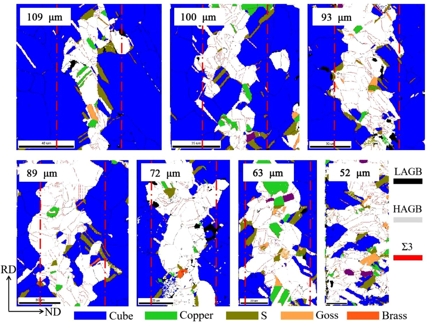
The formation of non-cubic grains in the inner layer is mainly related to defects such as grain boundary migration and twinning. Figure 6 indicates that in the inner layer of the Ni5W/Ni9.3W/Ni5W composite substrates with various thicknesses, HAGBs have a relatively high content (exceeding 76%). In addition, the Σ3 twin boundary content also has a high proportion in the inner layer, fluctuating at approximately 50%, whereas the LAGB content has a low proportion. The foregoing occurs because the defects of the inner layer have a pinning effect on the migration of grain boundaries. The non-cubic-oriented grains in the inner layer only erode a small part of the grains at the interface and do not progress towards the RD direction of the surface layer or outer layer to cause extensive erosion. Moreover, Figure 6(d) shows that the average grain size in the inner layer is smaller than that in the outer layer. Figure 5 also indicates that the grains in the inner layer of the composite substrate are more finely divided, and the possibility of defects, such as dislocations, is higher. This condition is unfavourable for the migration of grain boundaries.
Volume fraction of grain boundaries for RD-ND cross section of Ni5W/Ni9.3W/Ni5W composite substrates with different thicknesses: (a) LAGB, (b) HAGB, (c) Σ3 twin boundaries, and (d) average grain size.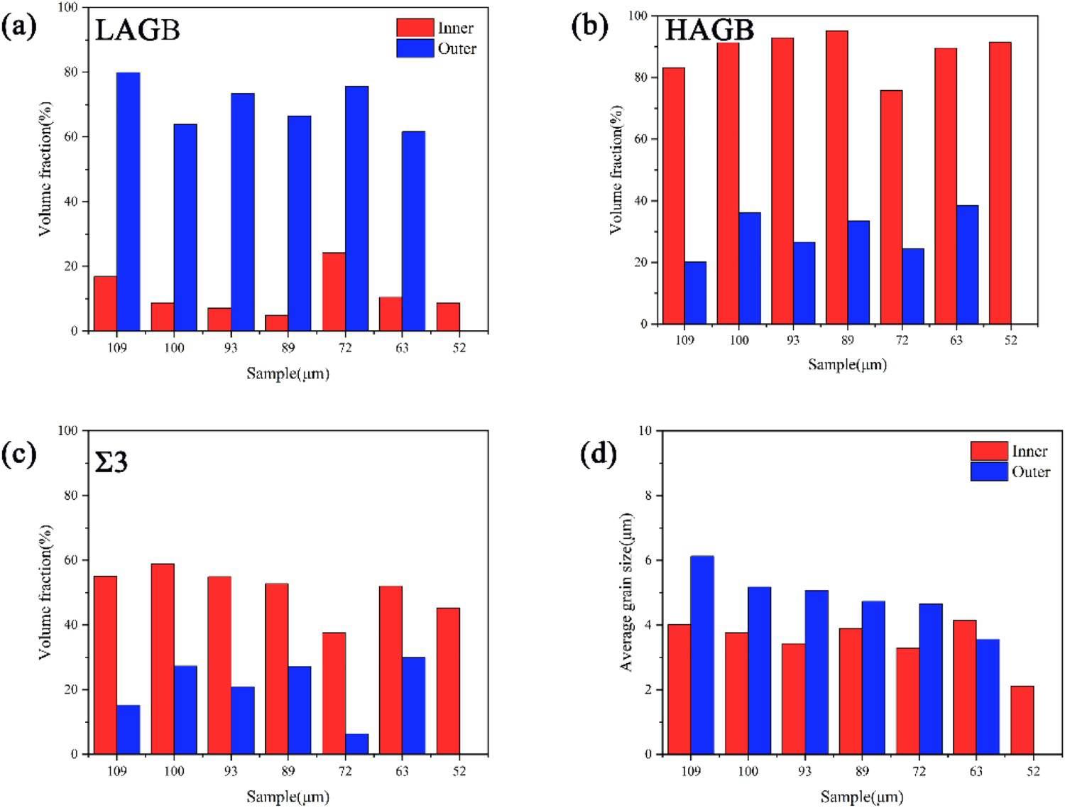
Overall, the defects in the inner layer have a ‘pinning’ effect on the migration of grain boundaries, and the growth of cubic-oriented grains in the outer layer tends to be more facile on the surface layer and along the RD direction. As the polishing time increases, the outer layer thickness of the Ni5W/Ni9.3W/Ni5W composite substrate continues to decrease; along the RD direction, the substrate progressively lengthens. Therefore, when the two-step recrystallisation heat treatment is performed, the cubic-oriented grains rapidly swallow the outer grains and those on the surface; the non-cubic-oriented grains are rapidly swallowed along the RD direction. When the thickness of the Ni5W/Ni9.3W/Ni5W composite substrate is 63 µm or less, the outer layer thickness is also small. Consequently, the non-cubic-oriented grains in the inner layer were not easy for the cubic-oriented grains in the outer layer to swallow. The formation of cubic-oriented grains from the outer layer to the surface layer was also difficult. Therefore, considering the thickness mentioned above, the overall cubic texture content on the RD-TD surface of the Ni5W/Ni9.3W/Ni5W composite substrate has significantly dropped.
Beyond the cube texture, the surface roughness is also important to the next epitaxial growth of the buffer and superconductor layers. The AFM images and the relevant RMS roughness are shown in Figure 7(a). It is clearly shown that along with decreasing thickness, the RMS surface roughness value also decreases. It is reasonable since the thickness is decreased by the electrochemical polishing process, the same polishing process as the others in which the goal is to polish the surface [19]. However, the surface roughness polishing has two obvious steps, and the thickness decreases, as shown in Figure 7(b). In the first step, the RMS surface roughness has a linear relationship with the thickness until the thickness reaches 72 µm. In this step, the main reason for the decrease in roughness is the removal of the small particles and the rolling groove. And then, the surface roughness barely changed and remained at a very smooth value of around 13 nm. It is may be that the chromium-free polishing solution H3PO4–H2SO4 can only polish to this level. If a more smooth surface is needed, other polishing solutions or even other polishing methods should be used. It is also worth mentioning that three different 20 µm × 20 µm areas were chosen in each sample during the AFM measurement. However, the grain size of the sample after annealing is basically over tens of micrometers. So we cannot guarantee that the roughness of the grain boundary is fully measured. More importantly, finding the grain boundary under AFM in the sample is quite hard. The grain boundary is covered by the rolling groove and the small particles at high roughness conditions. When the rolling groove and the small particles are removed by polishing, there is a possibility that the grain boundary is also polished simultaneously. Such a conclusion cannot be confirmed unless the comparison of AFM and EBSD is investigated. Since the grain boundary could be grooved during the cold-rolling process, which may also significantly affect the epitaxial growth of the buffer and superconductor layers, such a comparison investigation is our next investigation step.
(a) The AFM images of the Ni5W/Ni9.3W/Ni5W composite substrates with different thicknesses and (b) the relationship between the thickness and surface roughness.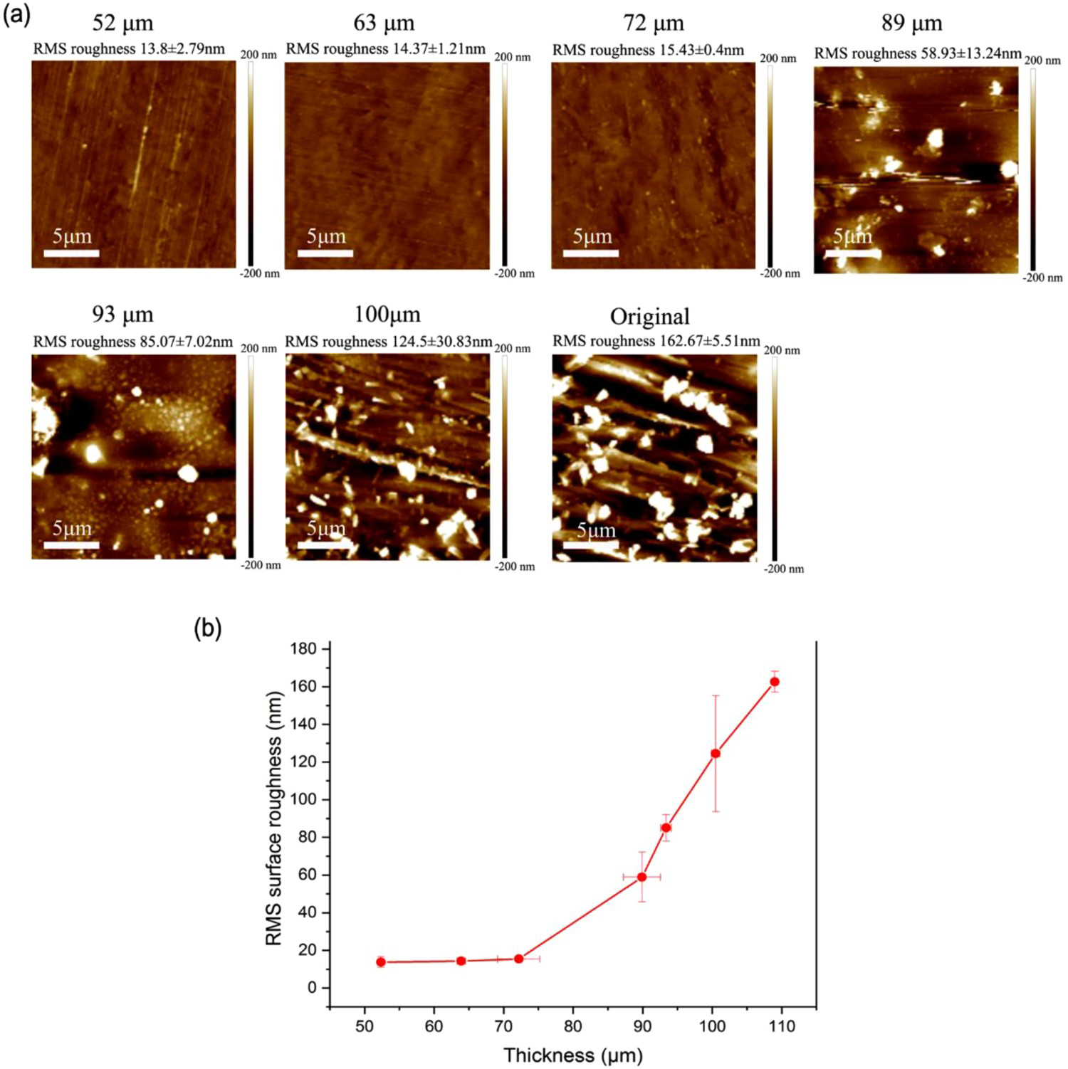
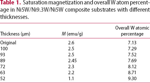
In the application of coated conductors to engineering, a metal substrate with a strong cubic texture at the bottom layer is required. In addition to this, the metal substrate's magnetisation must also satisfy certain requirements. This is because the ferromagnetism of the metal substrate can cause hysteresis losses when the coated conductor is applied in an alternating current field. Hence, the magnetisation of metal substrates is extremely important. Figure 8 shows the hysteresis loops of several Ni5W/Ni9.3W/Ni5W composite substrates with different thicknesses after the two-step recrystallisation heat treatment at 750 °C for 1 h and 1250 °C for 2 h. The figure indicates that as the thickness of the composite substrate decreases, its saturation magnetisation gradually decreases. When the thickness is 63 µm, the decrease in saturation magnetisation is significant. When the thickness is 52 µm, the lowest saturation magnetisation value is reached. However, the cubic texture on the surface of the composite substrate with this thickness cannot satisfy the requirements. This study focuses on the magnetisation of the Ni5W/Ni9.3W/Ni5W composite substrate with a thickness of 72 µm. Its saturation magnetisation reaches 2.3 (emu/g), which is 0.3 (emu/g) lower than that of the unpolished 109 µm-thick composite substrates. The overall W atom percentage of the Ni5W/Ni9.3W/Ni5W composite substrates with different thicknesses is also calculated, as summarised in Table 1. The objective is to determine the W content in the composite substrate that is equivalent to that in the single-layer Ni–W substrate. When the thickness of the composite substrate is 72 µm, the overall W content is equivalent to that of the Ni8.1W alloy substrate. This shows that the Ni5W/Ni9.3W/Ni5W composite substrate obtained by electrochemical polishing has a strong cubic texture on not only the surface but also its lower magnetisation is nearer to the requirements for the practical applications of coated conductors. That is, the Ni5W/Ni9.3W/Ni5W composite thin substrate prepared by electrochemical polishing achieves the coordination and unity of the surface cubic texture and the overall magnetisation.
Comparison of saturation magnetization of Ni5W/Ni9.3W/Ni5W composite substrates with different thicknesses after recrystallisation heat treatment. Saturation magnetization and overall W atom percentage in Ni5W/Ni9.3W/Ni5W composite substrates with different thicknesses.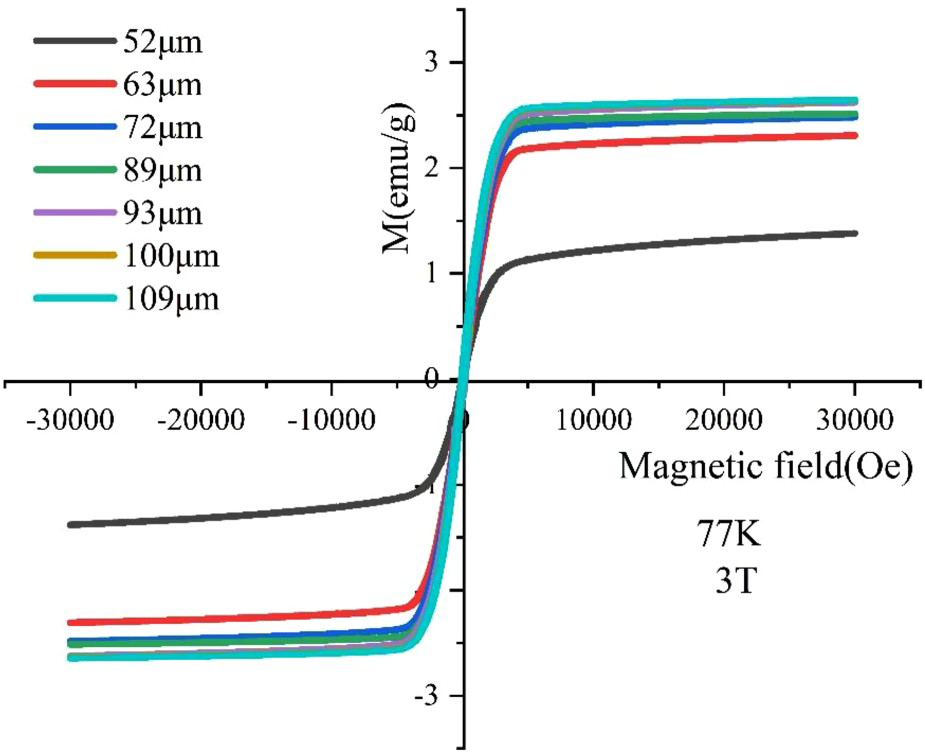
Ni8w/Ni12W/Ni8W composite substrate
The foregoing has analysed the polishing thinning of Ni5W/Ni9.3W/Ni5W composite substrates and the surface cubic texture, as well as the magnetisation of the thinned composite substrates with different thicknesses. The Ni5W/Ni9.3W/Ni5W composite substrate thinned by electrochemical polishing is found suitable for preparing coated conductors. Furthermore, the same electrochemical polishing process is employed to thin the Ni8W/Ni12W/Ni8W composite substrates. This verifies the universality of electrochemical polishing for thinning on different types of Ni–W alloy composite substrates.
Figure 9 shows the EBSD maps of the Ni8W/Ni12W/ Ni8W composite substrates with different thicknesses. In the figure, the grains of cubic texture are blue and all the other orientations are white. The cubic texture contents of the RD-TD surface of composite substrates with thicknesses of 85, 75, and 66 µm are 98.45%, 96.0%, and 94.7%, respectively. As the composite substrate thickness decreases, its surface cubic texture content exhibits a slight downward trend. In addition, the contents of HAGBs, LAGBs, and Σ3 twin grain boundaries on the RD-TD surface of the aforementioned composite substrates were also calculated, as shown in figure 10. Regardless of the substrate thickness, the content of LAGBs is consistently the highest, followed by that of HAGBs; the content of Σ3 twin grain boundaries is the least. When the thickness of the outer layer of the Ni8W/Ni12W/Ni8W/ composite substrate decreases, the LAGB content also slightly decreases. The content of HAGBs and Σ3 twin grain boundaries increase accordingly, correlating with the changes in the surface cubic texture content. This is consistent with the change rule of grain boundary content during the thinning process of the Ni5W/Ni9W/Ni5W composite substrate. The purpose of this experiment is only to verify whether the Ni8W/Ni12W/Ni8W composite substrate can also be prepared by electrochemical polishing; hence, the thinning of composite substrates with larger thicknesses is not performed. Thus, the experiment demonstrates that when the thickness of the Ni8W/Ni12W/Ni8W composite thin substrate is 66 µm, its surface cubic texture also exceeds 94%, fundamentally satisfying the requirements for preparing coated conductors. Accordingly, the following are observed. The electrochemical polishing method can be used to produce NiW alloy thin composite substrates. Preliminary observations indicate that the obtained composite substrate is suitable for the subsequent preparation of coated conductors (Figure 10).
EBSD maps of Ni8W/Ni12W/Ni8W composite substrates with different thicknesses after two-step recrystallisation heat treatment. The grains of cubic texture are blue in color and black in black and white and all the other orientations are white. Volume fraction of LAGB, HAGB and Σ3 twin boundaries for the RD-TD surface of Ni8W/Ni12W/Ni8W composite substrates with different thicknesses.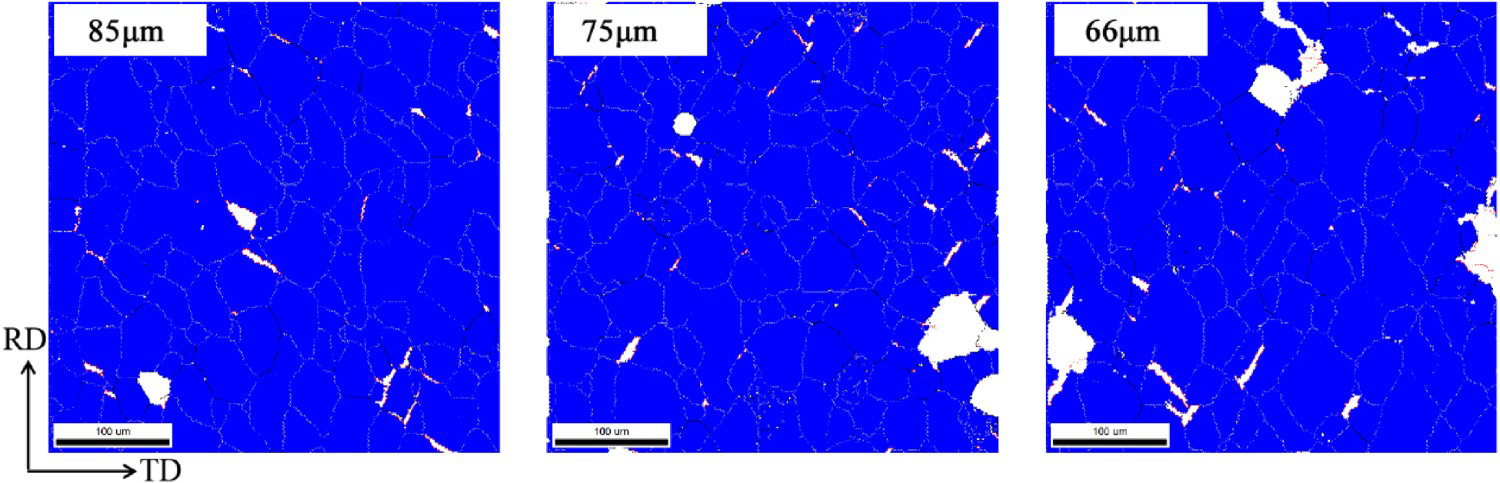
Nucleation mechanism
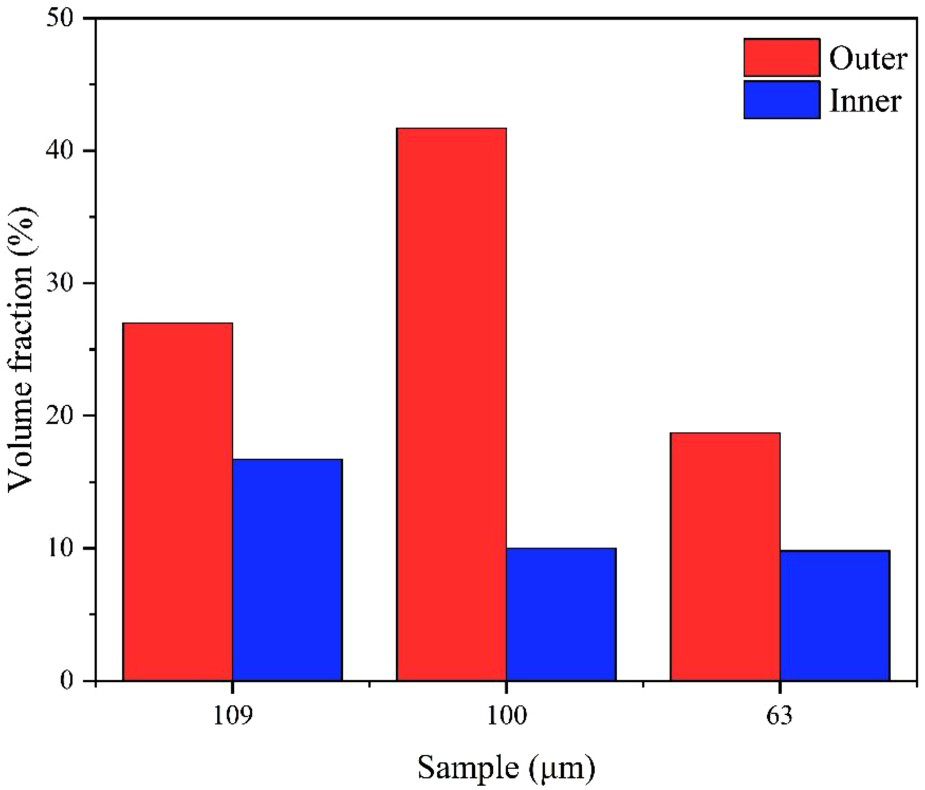
The foregoing study proves that the thin composite substrate has a strong cubic texture and lower magnetisation value after two-step annealing. In this annealing treatment, the nucleation process in the first step (750 °C/1 h) is extremely important. To examine this step, we selected the unpolished 109 µm-thick Ni5W/Ni9.3W/Ni5W composite substrate, 100 µm-thick lightly polished composite substrate, and 63 µm-thick composite substrates whose outer layer is approaching complete disappearance. These samples were heat treated at 750 °C for 1 h in the protective atmosphere of Ar–4%H2. The EBSD technique was employed to test the RD-ND cross-sections of the Ni5W/Ni9.3W/Ni5W composite substrates with the aforementioned thicknesses. After heat treatment at 750 °C for 1 h, some grains were recrystallised, and cubic-oriented grains were formed in the three composite substrate samples, as shown in Figure 11 (EBSD orientation maps). The unpolished 109 µm-thick composite substrates formed more cubic-oriented grains in the outer layer compared with the small quantity of these grains in the inner layer. Remarkably, some of the grains in the outer layer begin to merge with those in the inner layer, subsequently affecting the orientation of cubic grains in the inner layer. This observation is consistent with the grain trend after the two-step recrystallisation heat treatment shown in Figure 3. When the thickness of the Ni5W/Ni9.3W/Ni5W composite substrate is reduced to 100 µm, numerous cubic-orientated grains remain in the outer layer. According to the classic recrystallisation investigation of FCC metal with severe plastic deformation, the cube orientation has an obviously higher growth rate than the others [20,21]. So during the recrystallisation process, the cube grains tend to absorb other grains to grow bigger. Some of the grains begin to pass through the interface between the outer and inner layers and absorb the non-cubic grains in the inner layer. The formation mechanism of the cubic texture of the Ni5W/Ni9.3W/Ni5W composite substrate after polishing up to a thickness of 72 µm can be inferred as mainly dependent on the absorption of the outer cubic-oriented grains into the inner layer and the continuous growth along the RD direction. However, when the outer layer thickness is overly thin, heat treatment cannot promote the formation of cubic grains in the outer layer. Consequently, the cubic texture content of the composite substrate surface is extremely low after heat treatment. As shown in Figure 11, the EBSD orientation of the 63 µm-thick composite substrate shows that after the first step of heat treatment, only a small quantity of grains in the outer layer transforms into cubic orientation. Some grains begin to absorb the non-cubic-oriented grains in the inner layer. Moreover, Figure 12 shows that when the outer layer of the 63 µm-thick composite substrates is substantially reduced, this layer becomes unable to form a high quantity of cubic grains. The absorption of the inner layer becomes difficult for the outer layer such that the overall cubic grain content of the composite substrate is low. Furthermore, the combination of grain orientation spread (GOS) and kernel average misorientation (KAM) maps, as well as the identification of grain boundary in the orientation maps [21] indicates that a considerable amount of the residual stress generated during the rolling process remains and is distributed at the grain boundary. The internal stress is completely relieved after the final recrystallisation heat treatment. In addition, no distinct difference in the stress distribution between the outer layer and inner layers is observed. However, in the RD-ND section of the Ni5W/Ni9.3W/Ni5W composite substrate after heat treatment at 750 °C for1 h, the content of HAGBs is the highest, followed by the Σ3 twin grain boundary content; the content of LAGBs is the lowest (Figure 13). At this point, no significant difference in the grain boundary content between the inner layer and outer layers is observed. Under low-temperature heat treatment, the internal stress remains relatively concentrated and a considerable amount of stored energy has not been released; consequently, the grain boundary movement is not evident. However, as shown in Figure 13(d), the average grain size in the outer layer is consistently larger than that in the inner layer. This indirectly indicates that the absorption of the inner layer is facile for the outer layer.
EBSD orientation and GOS and KAM maps of RD-ND cross section of 109, 100, and 63 µm thick Ni5W/Ni9.3W/Ni5W composite substrates after heat treatment at 750 °C for1 h. Cubic grain content of inner and outer layers of the Ni5W/Ni9.3W/Ni5W composite substrate with thickness of 109, 100, and 63 µm. Volume fraction of grain boundaries of RD-ND cross section of Ni5W/Ni9.3W/Ni5W composite substrates with different thicknesses after heat treatment at 750 °C for 1 h: (a) LAGB, (b) HAGB, (c) Σ3 twin boundaries, and (d) average grain size.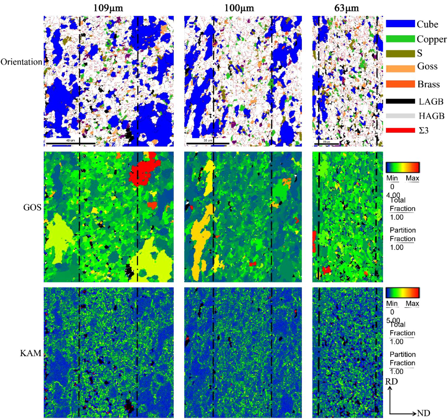
In summary, in the composite substrate outer grain in the two-step recrystallisation annealing process, the cubic-oriented grains facilely absorb the grains in the outer layer of the composite substrate, as other literature reported [22]. The cubic-oriented grains in the outer layer absorb the non-cubic-oriented grains in the inner layer with the migration of grain boundaries. Moreover, constant annexation in the outer layer along the direction of the RD grain growth is partly established by grain orientation. Concurrently, more twin grains exist in the inner layer. According to the pinning mechanism, these defects hinder the incorporation of cubic-oriented grains into non-cubic-oriented grains. Hence, a small amount of cubic-oriented grains in the inner layer does not achieve growth over a wide area; consequently, the cubic texture content is low.
Conclusion
In this study, we successfully prepared Ni5W/Ni9.3W/ Ni5W and Ni8W/Ni12W/Ni8W composite thin alloy substrates by the electrochemical polishing thinning method. The thickness of the Ni5W/Ni9.3W/Ni5W composite substrate was reduced to 72 µm. The substrate had a strong cubic texture of 97.3%. Moreover, its saturation magnetisation only reached 2.3 (emu/g), which considerably satisfies the requirement for preparing coated conductors. The Ni8W/Ni12W/Ni8W composite substrate, polished to a thickness of 66 µm, formed a relatively sharp cubic texture of 94%. A series of EBSD tests have proved that Ni–W alloy composite substrates can form a strong cubic texture when the outer layer is appropriately thinned. In summary, the thin 72 µm-thick Ni5W/Ni9.3W/Ni5W and 66 µm-thick Ni8W/Ni12W/Ni8W composite substrates can be applied to coated conductors, replacing an approximately 110 µm-thick composite substrate. The foregoing observations are anticipated to promote further advancement of the coated superconductor industry.
Footnotes
Disclosure statement
No potential conflict of interest was reported by the author(s).