
Abstract
The growth mechanism of various nanoforms of copper/copper silicide on Si substrates with different orientations is reported here. The triangular, square and rectangular copper/copper silicide nanostructures are deposited on silicon substrates with (111), (100) and (110) orientations respectively, by thermal evaporation of metallic copper at different substrate temperatures. Investigations confirm that the nanostructures consist of a pure copper layer on top of a copper silicide layer. The morphology and growth behaviour studies confirmed for the first time that the formation of well-defined structures and shapes are governed by the Si substrate orientation and the surface reconstruction of the Si planes. The copper silicide nanostructures are used in field emission applications and also serve as a template for the growth of carbon nano-fibre.
Introduction
Nanometre size self-assembled nanostructures on silicon are useful for contacts on molecular devices that have been of interest for the last few decades [1,2]. It has been found that surface reconstructed substrates may be used as a template for the oriented growth of metallic nanostructures [3–6]. Therefore, nanostructures of different morphology may be grown on substrates of a material cut along different orientations.
Copper metal, because of its higher electrical conductivity and electromigration resistance as compared to Al [7], is a promising material for interconnecting at the nano level. But, the easy diffusion of Cu in Si is an impediment to its use as interconnect material. On the other hand, it has been reported that the formation of copper silicide retards the effect of copper diffusion in silicon [8]. Thus the formation of copper nanostructure on the copper silicide layer (Cu/Cu3Si) supported on Si substrate is a possible candidate for metallic interconnects on future integrated circuits or nano-devices.
Though a lot of work has been reported on metal silicides, the Cu/Si system has not been investigated as thoroughly as other systems such as Ag/Si, Au/Si, Ti/Si and Pt/Si etc [9–15]. Ordered 2-dimensional (2D) Cu nanostructures on Si(111) have been reported for very low thicknesses by Zang et al. [16]. In the recent years, a huge volume of work has been reported on diffusion studies of Cu in Si substrates [17–41]. In most of the studies on the growth of Cu nanostructures on the silicon substrate, the films are deposited at room temperature and post annealed for preparation of nanostructures. Further, thickness of Cu films is limited to less than one monolayer. In all these reports, prior to deposition, the Si substrate is heated to around 1000°C in ultra-high vacuum conditions to remove the native oxide layer on the Si surface and enforcing surface reconstruction. Few reports are also available on the growth of self-assembled copper silicide nanostructures on various Si substrates at lower temperatures and poor vacuum conditions [31]. Parajuli et al. have reported self-aligned Cu3Si nanobeams on Si (100) substrate with an average width of 160 nm and length of 1.12 μm. They observed the initial growth of square-shaped structures followed by growth along the preferential direction to form aligned nanobeams. The width and length of nanobeams were tuned by changing the growth time. They have attributed the ordered and directional growth due to the orientational relationship between Cu3Si and Si where Cu3Si(010)[100]||Si(001)[110]. On the contrary, Zhang et al. [32] have grown nano-sized triangle, square and rod on Si substrate with an oxide layer using Au nanoparticles as template at 850°C and 20 mbar pressure. In this work, the Au nanoparticles were found to assist in the diffusion of Cu across the native oxide layer to form Cu3Si. Similarly, Benouattas et al. have described the role of the oxide layer in the formation of copper silicide [32,33]. Thus, it is evident that the growth mechanism of Cu3Si on Si substrate is neither well understood nor properly investigated. The actual growth behaviour of these structures and the effect of Si substrate orientation on the shape of the resulting structures need to be studied and understood.
In the present study, we report the growth of self-assembled Cu/Cu3Si nanostructures on the Si substrate. The growth of the nanostructures was carried out on the native oxide layer on the Si substrate at comparatively lower substrate temperature ∼750°C and vacuum condition without using any template or catalyst. It is observed that due to increased diffusion of ad-atoms at high temperatures, the structures formed are more uniform. These experiments for the first time show that the shape of the nanostructures is governed by the orientation of the Si substrate and has no effect on the presence or absence of the oxide layer and any form of catalyst. The growth mechanism of these structures has been discussed on the basis of a surface reconstruction of Si substrate to have a proper understanding and attain control over the growth process. Further possible applications of these structures for field emission application and as the template for carbon fibre growth are discussed.
Experimental
Deposition of Cu thin film on Si substrates of (111), (100) and (110) orientations was carried out by thermal evaporation at different substrate temperatures. Polished silicon substrates (n type) having resistivity in 1–10 ohm cm range were used and the depositions were carried out using high purity (99.9%) Cu metal strip which was evaporated from a tungsten filament inside a vacuum system. Before thermal evaporation, the Si substrates were ultrasonically cleaned in organic reagents like trichloroethelyne, methanol and acetone. Few of the substrates were also etched in HF solution to remove the native oxide layer. For accurate control of temperature, the substrates were mounted on a heater using thermally conducting silver paste. The vacuum chamber was evacuated by a turbo molecular pump to a pressure of 2 × 10⁻⁶ mbar. Prior to the depositions, the substrates were heated at 750°C for 2 h to degas all impurities and prepare a clean surface. Subsequently, the temperature of the substrates was set as desired for deposition. The depositions were carried out at a rate of 1 Å s−1 maintained using a quartz crystal thickness monitor and the thickness of the Cu layers was varied from 1 to 50 nm.
The surface morphology of the deposited films was studied using scanning electron microscope (SEM) VEGA MV2300T/40 (TS 5130 MM TESCAN) and atomic force microscopy (AFM) model JEOL JSPM 5200 used in a contact mode. The structural information was obtained by grazing angle X-ray diffraction carried out by employing a Cu Kα source. X-ray photoelectron spectroscopy measurements were carried out on a RIBER make model EVA-32 R&D molecular beam epitaxy deposition system with an attached XPS chamber. Al Kα source and a MAC-2 electron analyzer were employed for recording the spectra. The binding energy scale was calibrated to Au 4f7/2 line of 83.9 eV. For XPS analysis, the sample was loaded in high vacuum chamber immediately after deposition to minimise oxidation of the surface. TEM studies were carried out using the JEOL 2010 UHR system. The images were recorded using a 20X Gatan camera. For TEM measurements, the sample was prepared by cutting the Si substrate in a 3 mm diameter disc that was thinned to 100 nm thickness by grinding followed by a dimple cutter and Ar ion milling.
The field emission current density versus applied field (J–E) and emission current versus time (I–t) measurements were carried in all metal field emission microscope at a background pressure of ∼1 × 10⁻⁸ mbar. The field emission studies were carried out in a ‘close proximity’ (also termed as ‘planar diode’) configuration, wherein the Cu/Cu3Si on Si substrate served as a cathode and a semi-transparent cathodoluminescent phosphor screen as an anode. The current density versus applied field (J–E) and the emission current stability (I–t) measurements were carried out at this base pressure using a Keithley 6514 electrometer and a Spellman high voltage DC power supply.
Results and discussions
Initially, the Cu film depositions were carried out at different substrate temperatures in the range between room temperature and 850°C on Si (111) substrates and the morphology of the deposited film was investigated using SEM. Typical results for 10 nm thick films deposited at different temperatures and those deposited at room temperature (25 nm) followed by post annealing at 750°C are shown in Figure 1. Films deposited at low temperatures (500–600°C) including those annealed after deposition showed small and irregular size structures. This may be due to the small mobility of atoms at low substrate temperatures. Similarly, during post deposition annealing the mobility of deposited atoms is limited which hinders the formation of definite structures. Deposition at high substrate temperature around 800°C has yielded irregular and very small structures which may be due to re-evaporation of Cu atoms due to high kinetic energy acquired from the substrate. This is similar to findings reported for other metal silicides [10–15]. During in-situ deposition at optimum high substrate temperatures, the deposited ad-atoms have sufficient energy to find equilibrium positions leading to well-defined features. The depositions at 750°C substrate temperature were found to yield quite regular pattern and defined microstructures and all further experiments were performed at this substrate temperatures. Other orientations of Si substrates, i.e. (100) and (110) were also employed and oriented growth of regular patterns was observed on all the substrates at 750°C deposition temperature.
SEM micrographs of 10 nm thick Cu films deposited on Si(111) substrates at various substrate temperatures of (a) 500°C, (b) 600°C, (c) 750°C and (d) 800°C. (e) SEM of 25 nm Cu film deposited at room temperature on Si(111) and post annealed at 750°C.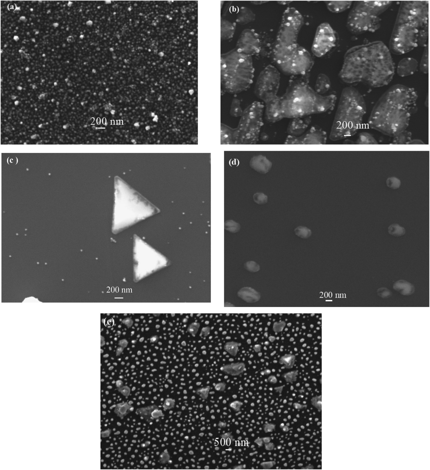
Typical SEM micrographs of films (with nominal thicknesses of 15 and 1 nm) deposited at 750°C on substrates with different orientations are shown in Figure 2. We find predominantly triangular, square and rectangular (nanorod) shaped nanostructures on (111), (100) and (110) Si substrates, respectively. On Si (100) oriented substrates, a few rectangular islands were also observed. These nanostructures are quite uniformly distributed on the substrate and on a given substrate they have fairly uniform dimensions. The size of nanostructures was found to increase with the increase in deposition thickness. Furthermore, edges of all the structures were found to be parallel to each other on each of the substrates. This indicates that the well-defined orientations of the nanostructures are supported by the crystallographic planes of the substrates in-spite of the presence of a native oxide layer on the substrate. In case of growth on HF-cleaned Si substrates where the native oxide was etched out, the edges of these nanostructures were found to be sharper as compared to those grown on un-etched substrates (images not shown). From this observation, it can be inferred that if the films are deposited on Si substrate with a thicker oxide layer the edges of the structure will be more diffused. However, it needs to be checked that till what thickness of SiO2 thickness the growth of oriented nanostructure is supported and is currently under study. Also, as the films are deposited at high substrate temperature and also all the substrates are baked at high temperature prior to film deposition, the presence of the oxide layer is negligible irrespective of substrate being ether or not.
SEM micrographs of Cu films of 15 nm thickness deposited on silicon substrates of (a) Si (111), (b) Si (100) and (c) Si (110) orientations. Depositions were carried out at substrate temperature of 750°C. Insets show SEM of films with lower thickness of 1 nm under identical deposition parameters.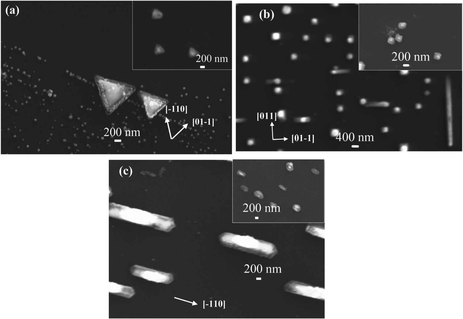
To further investigate the shape of the nanostructure, the films were probed by AFM and the results are shown in Figure 3. It is observed that the top of the nanostructures is not flat and they have larger thickness at the centre giving them a pyramid kind of shape. The typical height of structures was seen to be ∼150 nm for a nominal deposited film thickness of 1 nm.
AFM images of 10 Å thick Cu film on (a) Si(111), (b) Si(100) and (c) Si(110) substrates.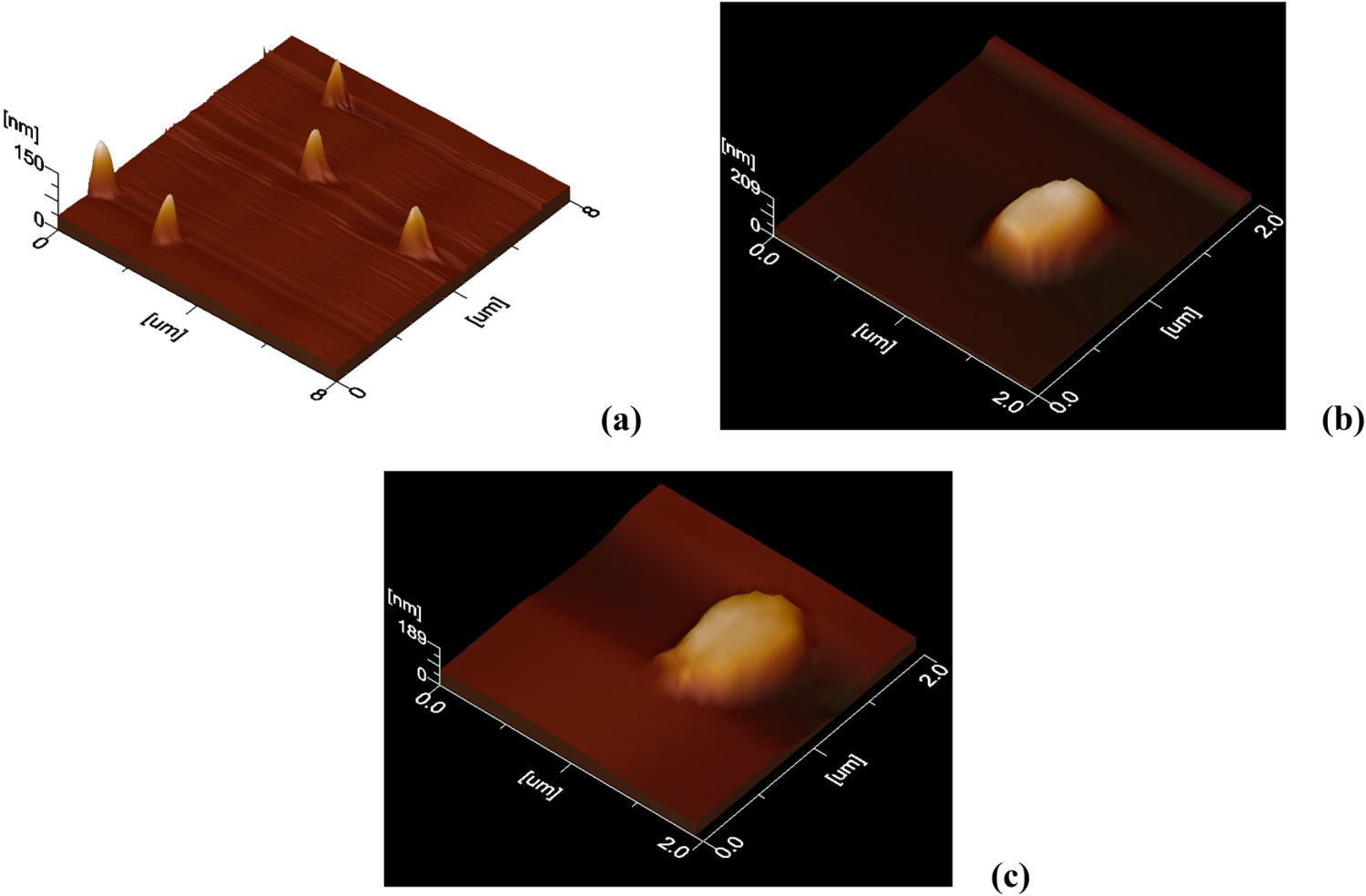
The details of the structure of a Cu nano pyramid on Si (111) were observed using high-resolution transmission electron microscopy (TEM) and the results are shown in Figure 4. TEM image of two triangular structures is shown in Figure 4(a). The corresponding lattice image at the edge of the nano pyramid is shown in Figure 4(b). We can observe two clear sets of lattice fringes in this figure. Upon proper investigation and indexing, we find that one of the lattice planes corresponding to Cu3Si and the other corresponding to the Cu structures. The spacing between the diffraction planes on the left side of the figure corresponds to Cu (200) plane with distance of 1.76 Å and on the right side is from Cu3Si(012) with lattice spacing of 2.06 Å [41]. Figure 4(c) shows the selected area electron diffraction (SAED) pattern of an individual pyramid. The SAED pattern confirms that the pyramids are crystalline in nature. The SAED pattern shows two sets of fringes which are consistent with the FCC structure Cu (200) and Cu3Si (012), respectively [41].
TEM of 200 Å thick Cu film on Si (111) substrates at 750°C (a) morphology of two aligned as deposited Cu nanoparticle. (b) HRTEM image of the Cu3Si (012) and Cu(200) lattice plane. (d) Selected area diffraction pattern of a single triangular nanostructure of Cu/Cu3Si.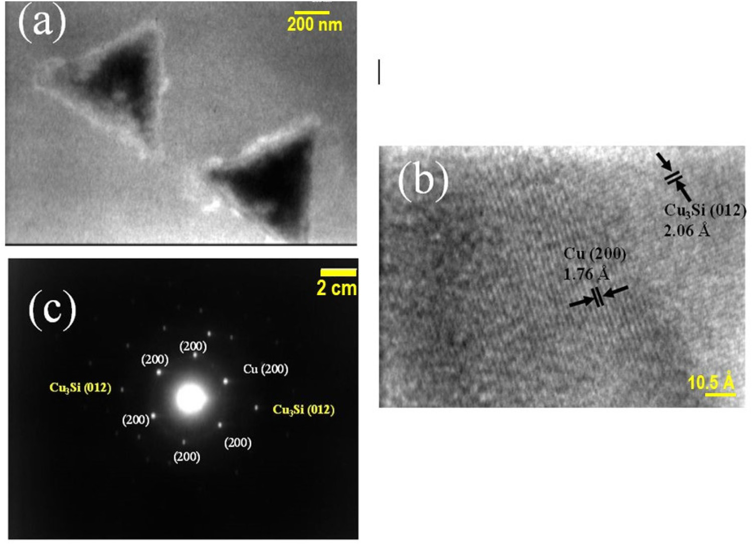
Grazing angle X-ray diffraction data of 30 nm thick films deposited at 750°C on different orientations of Si substrates are shown in Figure 5. Films of higher thickness were employed to obtain good peak intensity. Peaks corresponding to Cu3Si and small intensity peaks of metallic copper are seen for all substrates. It signifies interaction of Cu with substrate yields copper silicides and is in agreement with earlier studies [6,30–32,41]. XRD spectra also show the presence of un-reacted metallic copper present to be top surface of nanostructures as indicated by TEM and confirmed by XPS spectra discussed below. This result is very significant, as in all the metal silicide work, the presence of pure metal layer on the top has never been reported. Also, this shows that this kind of structure can be used as Cu metal interconnects in nano-devices.
Grazing angle XRD spectra of 30 nm Cu film deposited at 750°C substrate temperature on (a) Si(111), (b) Si(100) and (c) Si(110).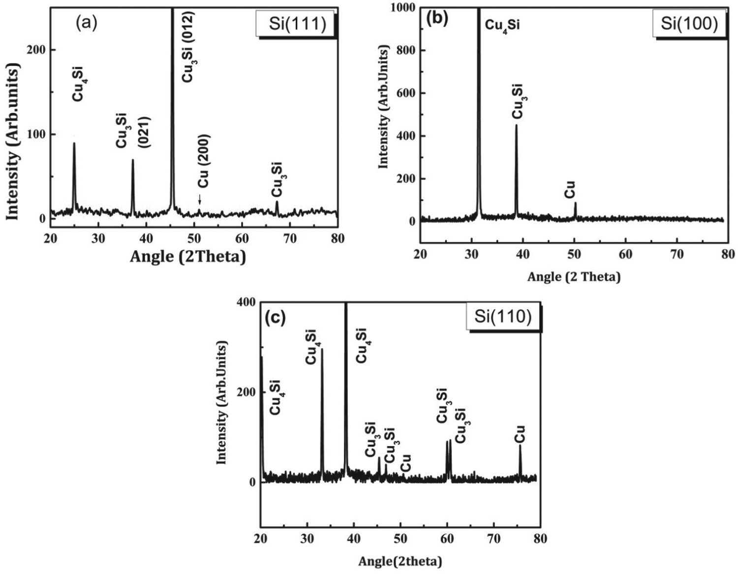
Figure 6 shows the XPS spectra of a Cu nano pyramid deposited on Si(111) substrate. Figure 6(a) is that of Cu 2p peak. The binding energy corresponds to that of pure Cu. It can be further seen that there is no signature in the formation of either copper oxides (absence of satellite peak) or copper silicide on the Cu 2p peaks. Since XPS is a surface-sensitive analysis technique with a depth analysis of just 10 nm, it is assumed that the surface of our sample is pure copper. As we have got copper silicide peak in the XRD data, it is confirmed that initially at the interface of the Cu film and Si substrate, there is a formation of copper silicide layer however the top layer of the nano pyramids is that of pure copper metal. This is because the formation of the copper silicide layer retards the further diffusion of Cu into Si substrate [7]. As the thickness of the Cu film increases the top portion of the nanostructure is pure metal. This was further confirmed by studying the Auger parameter of the Cu peak in Figure 6(b) which also matches to that of metallic copper [41,42]. The oxygen 1s peak in Figure 6(c) also shows the absence of copper oxide. However, we get a peak in oxygen 1s corresponding to SiO2. This is expected, as we have not etched the native oxide layer on the Si substrate prior to deposition. Si-2p spectra in Figure 6(d) have two peaks with binding energies around 99 and 102.7 eV. Peak with BE of 102.7 eV is attributed to thin silicon oxide layer on silicon substrate where Cu is not deposited and peak at 99 eV [43].
XPS spectra of a typical Cu film deposited on Si(111) at 750°C (a) Cu 2p, (b) Cu Auger, (c) O 1s peak and (d) Si 2p.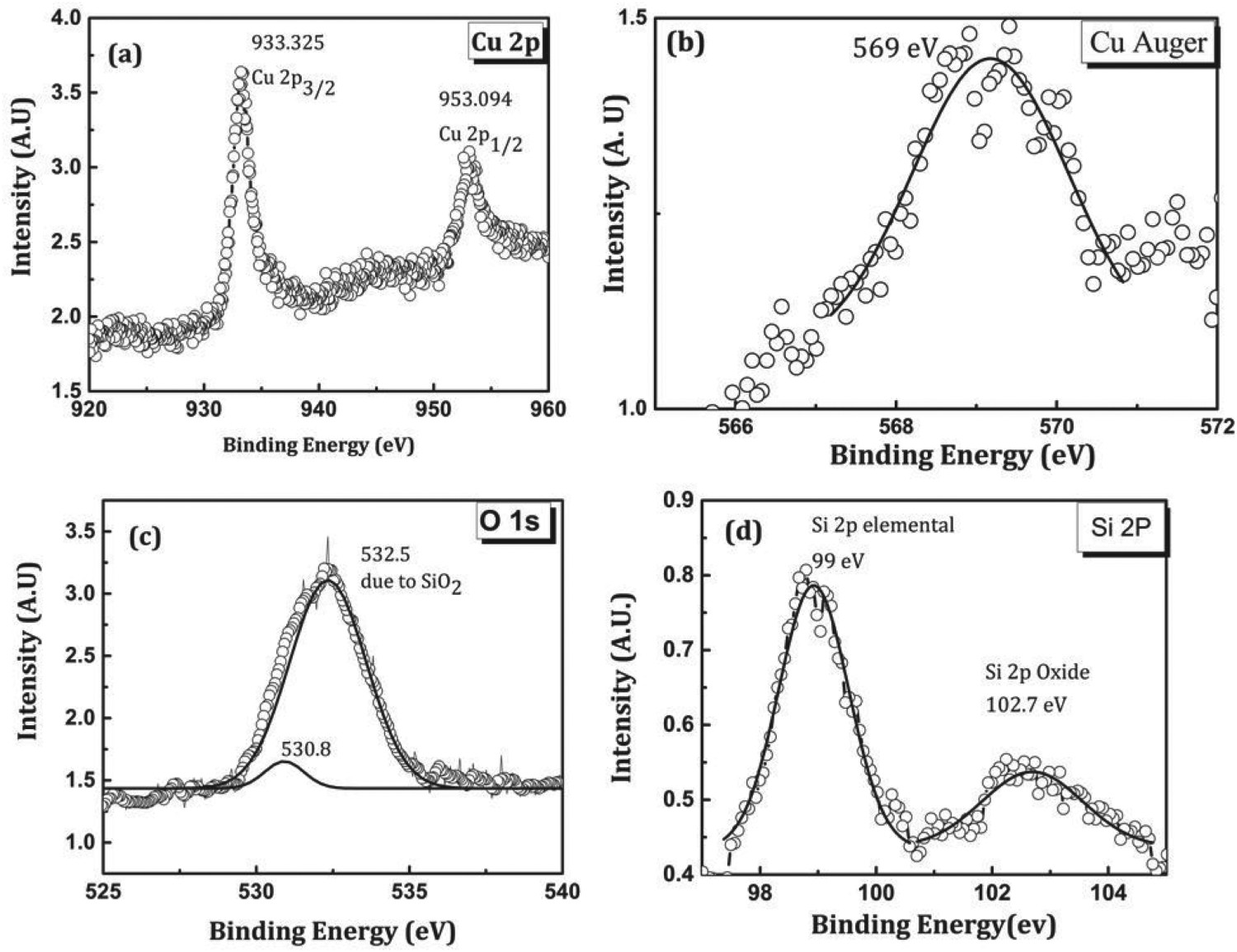
From the SEM and TEM micrographs, it is confirmed that the edges of the nanostructures are well aligned with some crystallographic axis of the Si crystal. The orientation of these nanostructures on the silicon substrate was identified by observing the alignment of the sides of the structures with respect to flats on Si substrates. In case of Si(111) substrates, the sides of the triangle were found to be oriented along the [−110], [01−1] and [−101] directions. This is similar to the reported formation of Gold silicide islands on Si(111) [43]. In case of nano-squares and nanowires on Si(100) substrate their sides were found to be oriented along [011] and [01−1] as reported in the formation of copper silicide nanobeams [37]. On the Si(100) substrates, we have also observed few islands elongated in one direction indicating tendency for 1D growth. Here, the square nanostructures get elongated leading to the growth of nanowire-like growth on the Si(100) surface at few places [44]. On the Si(110) surfaces, we observe growth of hexagonal-shaped rods with long axis of all rods parallel to each other. As the Si(110) substrates available with us did not have flats, the growth direction of wires could not be directly identified. We note that Si (110) substrate has a twofold rotation symmetry. Observation of rods along one direction only indicates that the long axis could be parallel to [−1 1 0] or [001] axis. In a recent study, dysprosium silicide on Si(110) is reported to grow in the form of nanowires with long axis along [−1 1 0] direction [45]. Therefore, we may expect growth along this axis. The schematic diagram of a rod is shown in Figure 7. The growth along this axis is further supported by measurement of angle α. A value of ∼ 55° indicates that the growth of nanowires terminates on edges parallel to [−1 1 2] and [−1 1 −2] directions. The Si substrate-dictated shapes of the structures are consistent with previous reports. Furthermore, our studies give insight into the growth direction of these structures on the Si substrate and can be very useful information for site-specific applications. The observed orientations of the different structures are similar to that reported by Zhang et al. [32] where they have grown similar structures on Si substrate with an oxide layer using Au nanoparticles as a catalyst. But in our case, we have not employed any catalyst which simplifies the growth procedure and also prohibits the addition of any impurity from the catalyst.
Schematic diagram of Cu3Si nanowires deposited on (110) oriented substrates. The angle α determined from SEM was measured to be varying between 50° and 60° for different wires with average value of ∼55°. Theoretically calculated angle is expected to be 54.7°.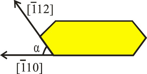
Thus, all our experimental results point to the fact that very definite nano-patterns are formed which are dictated by the orientation of the underlying Si substrate. This observation has been reported by many groups and for different metallic silicides. Our study also supports that on top of the interfacial layer of copper silicide, we get pure metallic layer which has significance in device applications. But the fundamental reason for the growth of specific structure is still not understood and most of the groups have not tried to explain this. In the following section, we have tried to understand the growth mechanism of the island structures and the probable reason for them acquiring definite shapes.
Understanding growth behaviour
Some of the interesting observations that may elucidate the growth mechanism are (a) shape of the structures (triangles observed in Figure 2) is better defined (sharper) as the thickness increases and (b) structure being rounded with larger thickness at the centre (confirmed by AFM Figure 3). We propose that the rounding of edges for films with smaller thickness occurs due to re-evaporation of atoms from the islands as the ad-atom pressure is reduced and because the triangular-shaped islands are kinetically driven (during growth) with hexagonal shape being thermodynamically more stable. The effect of this post growth atomic migration is reduced on thicker and wider islands leading to their better defined triangular shape. The growth of thick islands before agglomeration of nuclei may be attributed to higher energy barrier for nucleation of a new row along the triangle edges in comparison to nucleation and growth in the next layer. The round shape of islands as seen in AFM may be caused by need to minimise their free energy [46,47]. We may note that the 3D island growth seen here is in contrast to layer-by-layer growth (on each island) seen for homoepitaxy [48–50].
Furthermore, in this study since no catalyst has been used, the vapour–solid mechanism is the likely mechanism responsible for the growth of different nanostructures. At the initial phase of deposition, the Cu vapour reacts with substrate Si and forms copper silicide [40,51]. The presence of an oxide layer on the Si substrate was neither found to hamper nor found to assist the interaction of Cu with the substrate [6]. Second, at elevated substrate temperature (750°C), the thickness of the native oxide layer is assumed to be very less or negligible. As per the Cu-Si phase diagram at a temperature around 750°C, the η−Cu3Si phase is formed which is supported by XRD peaks on all three substrates [50,51]. The inter-diffusion of Cu on Si substrate covered with native oxide has been reported to be very slow [52,53]. As in our experiments, the growth rate was controlled at 1 Å s−1 thus ample time is provided to the incoming Cu vapour to diffuse and react with the underlying Si. We have confirmed that no pattern formation is observed when the rate of deposition was increased to 5 Å s−1. Second, the AFM studies have shown that the total thickness of a particular island was found to be ∼150 nm, implying the initial formation of Cu3Si layer impedes further diffusion of Cu into the Si which gives the top layer of the islands as pure Cu [18,54].
It is highly interesting to note that the observed nano-pattern is only formed when the deposition is carried out at a substrate temperature of around 750°C. At temperatures around 500°C, we obtain spherical nanoparticles of Cu on all the Si substrates with different orientations. This shows that temperature is an important parameter irrespective of their orientation controlling the geometry in the growth of these patterns. When an epitaxial layer is grown on a substrate due to lattice mismatch the layer undergoes a strain. To relieve these strains, the layer forms islands, which is a widely known phenomenon [41]. However, the shape of these islands is dependent on the underlying substrate upto a certain thickness. With an increase in layer thickness, these strains decrease and ultimately the islands coalesce to form a continuous film even at high temperatures. This phenomenon has been confirmed by depositing a film of thickness of 1000 Å at 750°C. This film was found to be continuous in nature without the formation of any nano-pattern/islands. This gives an indication that the nano-pattern formation on the Si substrates at low thickness and a definite temperature range may be because of island formation to relieve strain and supported by the surface reconstruction occurring around 750°C. The pyramidal and layered structure of the nanostructures formed indicates that the growth occurs in the Stranski–Krastanov (SK) mode; where initially the growth of a monolayer takes place and then ad-atoms start nucleating on top of this layer. This growth process is similar to that observed by Chakraborty et al. [54] in case of growth of gold silicide on Si(111) surface. In the SK growth model, the substrate orientation influences the growth behaviour of these strained layers. Appropriate changes in substrate orientation induce different morphologies of islands for the same epitaxial film [48,49].
It must be noted that reports on Si surface reconstruction generally use atomically clean substrates, which are annealed at around 700°C for many hours and then flash heated to 1000–1200°C by passing direct current through them in UHV conditions [16,55,56]. In our study, we have heated all the substrates at 750°C for 2 h in the vacuum chamber prior to deposition. Some substrates were used with their native oxide layer and some were etched using the HF solution. However, we have not observed any difference in the pattern size and shape on both kinds of substrates. The only visible difference was in case of pattern formed on etched substrates the edges of the nano-patterns were very sharp.
The phenomenon of surface reconstruction is the rearrangement of atoms at the surface due to the termination of the bulk structure at the solid–vacuum interface has been extensively investigated. The surface reconstruction is motivated by the reduction of dangling bonds on the surface thus forming minimum energy states [3]. During the deposition of thin film atoms are deposited on sites of a regular lattice, migrate on the surface and nucleate islands that continue to grow and eventually complete a new atomic layer. However, surface reconstructions can drastically alter established patterns of the surface morphology evolution. The Cu metal atoms approaching the reconstructed surface (of Si in this case) encounter an attractive potential well, existing on the surface. The ad-atoms get trapped in these low-energy regions and form a regular array of clusters with well-defined shape, which is the shape of a unit cell in the reconstructed surface. The extra ad-atoms try to diffuse into this domain of lower energy so as to acquire minimum energy. This is the case when the thickness of the film is few monolayers or even less than a monolayer [57,58]. However, with the increase in thickness they start expanding over plural subunits and these islands are crystalline in nature. Thus, the formation of amorphous clusters is followed by the growth of crystallised islands as happens in our case [49].
Growth on Si(111) substrate: The reconstruction of Si(111) substrate occurs by the formation of dimers, ad-atoms and stacking faults in order to minimise the number of dangling bonds and leads to the formation of two dimensional rhombic unit cell with edges of 26.9 Å length [3,4,16]. The rhombic unit cell in turn consists of two triangular half unit cells (HUC), one with a stacking fault (HUC-F) and one without a stacking fault (HUC-U) with respect to the bulk. Two dimensional islands nucleate at the domain boundary of (7 × 7) reconstruction as atoms in this region have higher energy due to broken symmetry. The observation of triangular-shaped crystalline nanostructures and orientation of triangular edges along [-110], [01-1] and [-101] axes (edges of 7X7 HUC) support that this mechanism reported for homoepitaxy is applicable in the present case of growth of Cu on silicon as well.
Growth on Si(100) substrate: On Si (100) substrates, we observe the formation of square islands with some of the islands elongated in one direction indicating some tendency for 1D growth. The surface reconstruction on Si(100) leads to the formation of 2 × 1 unit cells that reduces surface energy by reduction in number of dangling bonds [39]. In the initial stages of growth, the atoms nucleate on the dangling bonds of the dimmer row and form a square nanostructure [9]. With increase in number of ad-atoms, due to high mobility along the dimmer rows and low across them, the arriving ad-atoms on island sides are transported to the ends [49], resulting in 1D growth. Thus, the square islands get elongated leading to the growth of Cu nanowire-like growth on the Si(100) surface at few places[16]. The length of these wires are found to be perpendicular to each other (Figure 2(b))because as the stacking sequence in the Si(100) substrate, the dimmers are rotated by 90° on two adjacent terraces separated by a monoatomic step [49,51].
Growth on Si(110) substrate: The formation of metallic structures on Si(110) substrates has not been much reported. On these substrates, we observe the growth of hexagonal-shaped wires with the long axis of all wires parallel to each other. It is reported that Si(110) substrates are expected to undergo 16X2 surface reconstruction with equivalent chains along [-1 1 2] and [-1 1 -2] directions.[59,60] If the growth occurred along the chains, we should have observed long axis along these two different directions with angle of 109.4° between them. However, as discussed in Figure 7, this is not observed. In a recent study, dysprosium silicide on Si(110) is reported to grow in form of nanowires with long axis along [-1 1 0] direction [45]. Therefore, we may expect growth along this axis. The growth of nanowires terminates on edges parallel to [-1 1 2] and [-1 1 -2] directions of chains for 1 × 16 reconstruction. This indicates that diffusion is faster along these chains compared to normal to the chain direction.
Thus, Si surface reconstruction explains the shapes and the geometry of the Cu nanostructures by providing minimum energy sites on the surface. The lowest energy basin has a particular shape depending on the unit cell of the reconstructed and the ad-atoms settle preferentially on certain crystallographic planes more strongly than the others. The extra ad-atoms try to diffuse into this lower energy so as to acquire minimum energy. It is also typically assumed that the atoms diffused into the low-energy configuration remain in that state unless an extra energy is provided to them to climb up the basin and diffuse into the next basin. This preferential adsorption lowers the surface energy bound to the plane resulting in the definite morphology of the copper nanoparticles with respect to the reconstructed silicon surface.
Application of Cu/Cu3Si nano pyramids
Field emission: To investigate the application of these nanostructures on Si substrate the field emission study of one of the samples, i.e. on Si(110) is carried [61–64]. The field emission studies were carried out in a planar diode (close proximity) configuration at background pressure of ∼1 × 10⁻⁹ mbar. An emission current density of ∼3 μA cm−2 has been drawn at an applied field of ∼4.6 V μmas−1 shown in Figure 8. The Folwer–Nordhiem plot showed a non-linear behaviour in Figure 8(b). The high value of field enhancement factor (β ∼1 × 10⁴), estimated from the slope of the F–N plot, suggests that the emission is indeed from the nanometric tips of the Cu/Cu3Si nano pyramid. The emission current stability studied at the preset value ∼1 μA over the duration of more than 2 h is found to be very good, suggesting the use of Cu nanorods as promising electron source for field emission-based micro/nano-electronic devices.
(a) Field emission current density versus applied field (J–E) curve of the nano pyramid of Cu/Cu3Si on Si(111) substrate recorded at base pressure of ∼1 × 10⁻⁹ mbar, (b) the Folwer–Nordheim (F–N) plot derived from the J-E curve and (c) field emission current–time (I–t) curve recorded at base pressure of ∼1 × 10⁻⁹ mbar at preset value ∼1 μA. In the inset field emission image of the nano pyramids of Cu/Cu3Si recorded at base pressure of ∼1 × 10⁻⁹ mbar.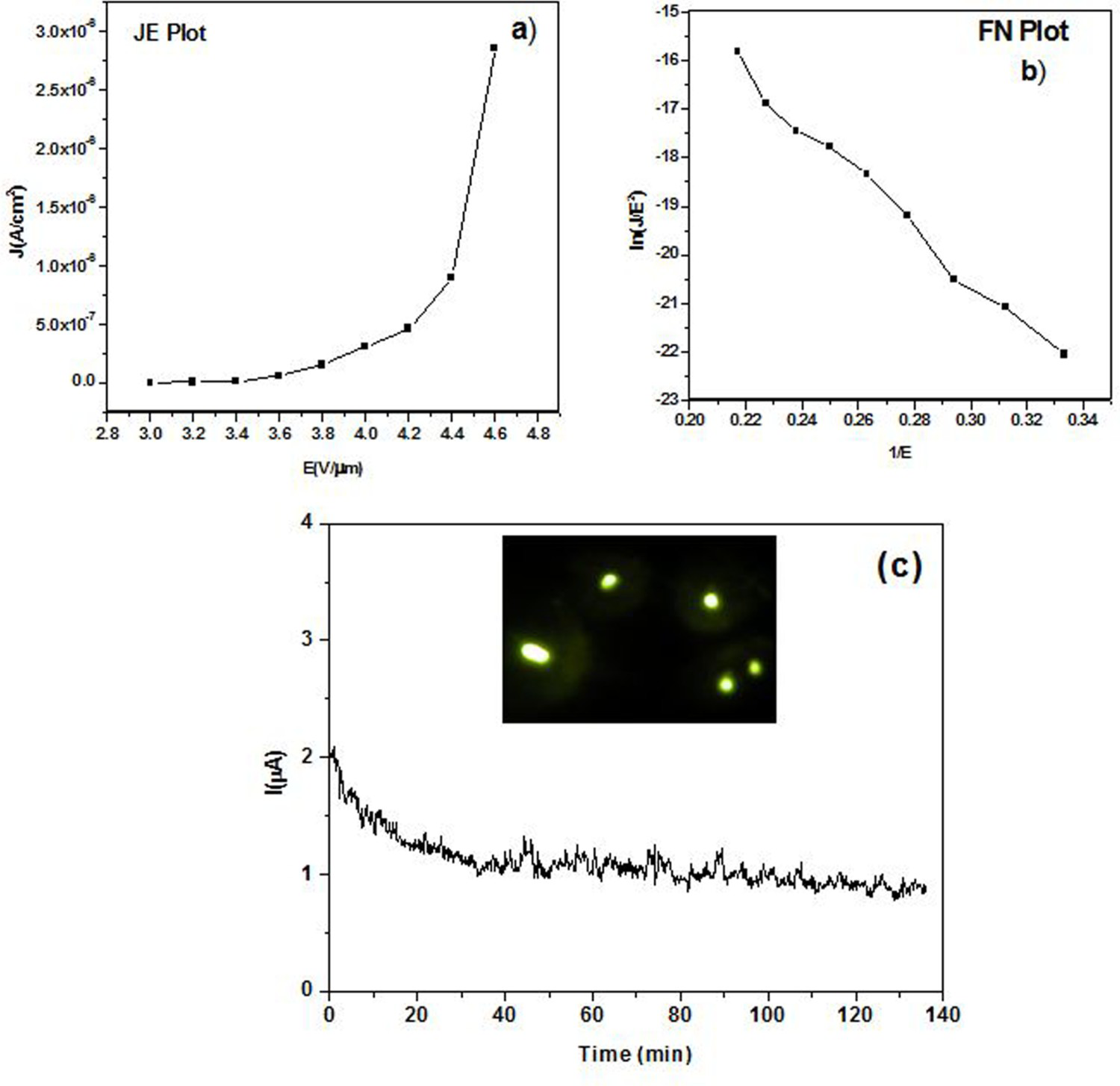
Template for carbon fibre: Furthermore, these nanostructures were investigated for use as templates for the growth of carbon nano-fibres (CNF) [31,65]. The Si substrate with Cu/Cu3Si structure was kept in a tubular furnace and heated to 800°C. The deposition of carbon fibre was carried out by flowing Ar gas through benzene into the furnace at a rate of 10 cc min−1. The deposition was carried out for 1 h. The Si substrate was characterised using SEM micrography and Raman spectra (Figure 9). The SEM spectra reveal that the nanao-structures are covered with CNFs with a diameter of about 50 nm. The carbon structure is rooted at the Cu/Cu3Si pattern and is tapering outward. The samples were characterised further by using Raman spectra. Typical features of the Raman spectra in the CNTs appear in the G band (1593 cm−1), originating from the graphite structure and D band (1351 cm−1) originating from the disordered carbon. The IG/ID ratio is a well-accepted index for fractional content of the ordered graphene structure within a carbonaceous sample. The IG/ID ratio is small in our case indicating the formation of much amorphous carbon structure known as CNF structures. The topic is under further study and the use of the Cu/CuSi nanostructure for CNT growth is experimentally checked.
(a) SEM of carbon fibres on Cu/Cu3Si structures. (b) Raman spectra of carbon nano-fibres.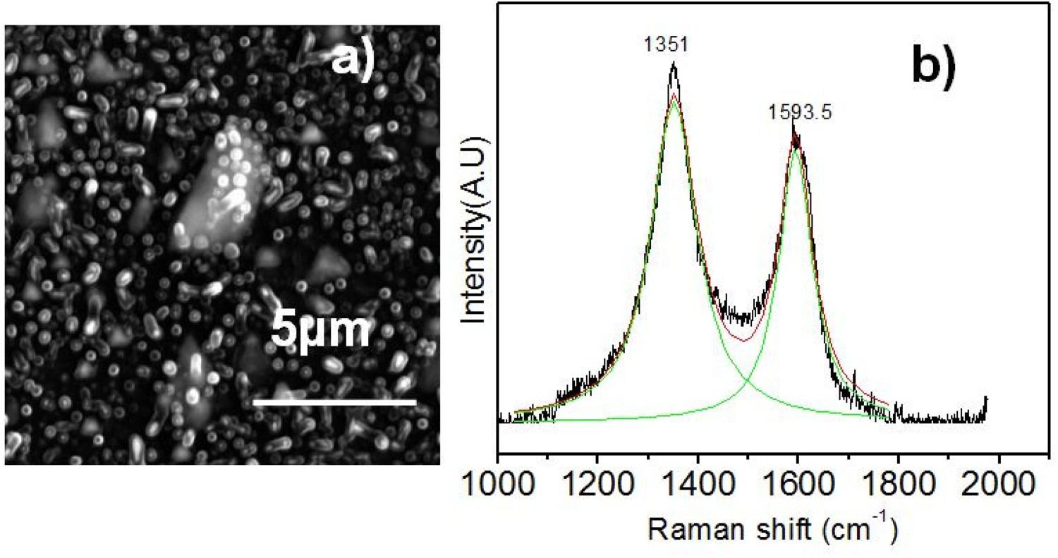
Conclusion
Oriented nano pyramids with the definite shape of Cu/Cu3Si on Si substrates with different orientations were grown and investigated by SEM, TEM, XRD and XPS techniques. (i) Nano-triangles were grown on Si(111) substrate, nano-hexagon on Si(110) and nano-sqaure was formed on Si(100) substrate. (ii) These structures were formed at a substrate temperature of 750°C under strict deposition condition. (iii) Change in deposition parameters like rate of deposition, film thickness, post deposition annealing did not yield the specific nanostructures. (iv) Studies verified that the shapes of these nanostructures were linked to the surface reconstruction of the Si substrate which is happening during annealing of the Si substrate at 750°C. (v) Investigations verified that the nanostructures have the base of Cupper silicide and the top was of pure copper. (vi) These nanostructures can be used as field emitters and have good long-term stability. (vii) These nanostructures can be used as a template for the growth of carbon nanostructures.
Footnotes
Acknowledgements
Authors are grateful to Dept of Physics, University Pune for FEM measurement and Professor P V Satyam, IOP Bhuwaneshwar, India for TEM measurements.
Disclosure statement
No potential conflict of interest was reported by the author(s).
Data availability statement
The raw/processed data required to reproduce these findings cannot be shared at this time as the data also forms part of an ongoing study.