
Abstract
NiO films were deposited on glass and Si(100) substrates by reactive pulsed laser deposition from the Ni target. Nd: YAG laser (1064 nm) was used. The oxygen pressure was between 0.05 and 0.3 Torr. The optimum conditions for a good-quality NiO film are an oxygen pressure of 0.1 Torr and a laser power of 410 mW. Preferred orientation changes from (200) to (220) and D decreases from 27 to ∼9 nm as the temperature increases from 200 to 300°C. The preferred orientation changes into (111), nanoparticles size reduces from 46 to 26 nm and D drops from 27 to 10 nm as laser power increases from 410 to 820 mW. The oxygen pressure is significantly affecting the composition and morphologies of the NiO films. The optical band gap was 3.35 eV.
Keywords
Introduction
Motivating in the investigations of nickel oxide, NiO thin film comes back due to its heavy use in wide industrial applications. NiO is one of the transition semiconductor oxides with a wide range of technological applications in many functional devices. Also, it exhibits interesting ferromagnetic properties even at room temperature [1–3]. The thin film form of NiO is a promising object for many applications, such as spin-valve giant magneto-resistance (GMR) sensors (magnetic head for writing and reading magnetic information) and electrochromic display devices. The display device includes a layer of photoconductive material and a layer of electrochromic material between electrodes. NiO nanoparticles as transition metal oxides with high surface area, as well as such unique optical and magnetic properties, had been considered as promising electrode materials for supercapacitors and high-power energy storage devices [3–5]. NiO optoelectronic applications are such as p-type transparent conducting electrodes and are used as inorganic hole transporting layer QD-LED [6–8].
The most attractive features of NiO are its low cost, and widely varying optical, chemical and magnetic properties depending on the synthesis technique and manufacturing conditions. Also, NiO is sufficiently stable at an elevated temperature which makes it withstand the high-temperature annealing and treatment processes.
NiO like many other metal oxides crystallises in the rock-salt (NaCl) FCC structure with a lattice constant of (a = 410 m7 nm). NiO is anti-ferromagnetic insulator with Néel temperature (TN) of 525 K and electrical conductivities in 10−15-10−17 Ω−1 cm−1 range [9]. The as-grown undoped NiO films are usually p-type resulting from excess Ni vacancies. Also, non- stoichiometric NiO is a p-type of semiconductor [6,10,11]. N-type conduction results if oxygen or Ni3+ vacancies became dominant. Many researchers show that the electrical conductivity of NiO films strongly depends on the formation of the structural defects such as vacancies and/or oxygen interstitial in NiO crystals [7,12].
The quality of NiO film is strongly influenced by both the kind and temperature of the substrate during the film growth. Several kinds of substrates have been used for NiO growth. So to grow epitaxial NiO with reduced strains and dislocation the lattice-matched substrates such as MgO (100) and sapphire substrates are commonly used. Other substrates such as Si and glass substrates were also used [4].
One of the effects of the substrate heating on the quality of the gown films is the increase in the gain size. Hence the larger the gain size the smaller the gain boundaries and that leads to better quality films. The variation in the gain boundaries also causes variation in the band gap of the NiO films [13,14].
Various physical and wet deposition techniques have been used to grow NiO in thin film forms. These techniques are RF magnetron sputtering,metal-organic chemical vapour deposition (MOCVD), sol–gel, thermal decomposition and pulsed laser deposition (PLD) [5,8,10,12,15,16]. Also, NiO films were synthesised by electrochemical precipitation method [17], chemical-vapour deposition (MOCVD) [12,18] and PLD [19]. The PLD technique has advantages compared to the previous techniques. The advantages are including its capability to grow high-quality film at lower temperatures with stoichiometry preservation [20]. Hence the ablation species from the target are travelling at very high kinetic energy so PLD is expected to reduce the growth temperature [19].
For PLD of NiO films (ns) lasers had been widely used, especially the ArF (193 nm) and KrF (248 nm) excimer lasers as well as the frequency tripled Nd: YAG lasers (355 nm).
There is not too much work on the deposition of NiO thin films by laser ablation using a Ni target. NiO thin films were deposited by laser ablation of Ni target in oxygen reactive atmosphere by using Nd: YAG pulsed laser that was operated at a wavelength of 1064 nm on different types of substrates as reported [21,22]. As it was reported that NiO was deposited by laser ablation of Ni targets in an oxygen atmosphere by a 355 nm pulsed laser on different types of substrates [10]. They studied the influences of the O2 pressure during the deposition process on the morphology, In their work, NiO films were obtained by reactive laser ablation of Ni target under an oxygen atmosphere on Si (100) substrates with an Nd: YAG laser of 355 nm wavelength as the pulse laser source. The electrical and sensing properties of the films are greatly affecting on the structure and optical properties of NiO film. Nanostructured nickel oxide films were prepared on quartz substrates under an oxygen partial pressure of 1.5 × 10⁻³ Torr but under very high substrate temperature [21]. Relatively very high laser power was used to prepare nickel oxide nanomaterials by Nd: YAG laser compared to the current work [22]. The properties of the film, such as the structure, optical, electrical and surface morphology, completely depend on the preparation method, deposition conditions and/or post-annealing conditions [10].
In this study, we investigated the structural, morphological and optical properties of NiO films grown on both Si(100) and bear glass deposited by PLD. The structural properties of NiO films on Si(100) were measured using X-ray diffraction (XRD), Atomic force microscope (AFM), scanning electron microscope (SEM) and transmission electron microscope (TEM).
Experimental
Pulsed Nd: YAG laser was operated at a wavelength of 1064 nm with a repetition rate of 10 Hz. The laser power is 410 and 820 mW and the pulse width (FWHM) is 18 ns. These laser pulses are introduced into a stainless steel ultrahigh-vacuum (UHV) PLD system chamber, 15 cm in diameter and 25 cm high, and focused on the target by a 75-cm focal length lens. The chamber is evacuated by a turbo-molecular pump and then an ion pump to abase a pressure of ∼3-5 × 10⁻⁸ Torr. A Ni circular plate (purity 3N) 1 in diameter and 0.125 in thick will be used as the target. The laser was incident on the Ni target at an incident angle of 45°. The target was rotated at a speed of 36 rev min−1 to minimise the possibility of any particulate formation and to ablate fresh surface homogeneously during the deposition process. The target-to-substrate distance was fixed at ∼ 4 cm. Once the desired vacuum is achieved the oxygen gas injection was achieved through stainless steel tubing, through an ultra-precision leak-valve. The oxygen partial pressure was adjusted during the deposition using the leak valve. NiO films were deposited on both glass and silicon substrates at oxygen (purity 99.99%) in the range pressure of 0.01-1 Torr in the static regime. Si 5 × 15 mm2 substrates were cut from a Si(100) wafer (n-type, doped, 500-μm thick). The Si(100) surface was prepared by chemical etching just before being loaded into the UHV chamber using a method which is explained in detail in [20]. The glass substrates cleaning was done by cleaning them with chemicals in ultrasonic. Acetone, methanol and DI water were used separately in ultrasonic for 5 min each. The substrate was uploaded into the chamber and the system was pumped down to the minimum pressure the ion pump could reach. A Valued Ocean Optics s2000 spectrometer model USB2E1225 was used to identify the lines of the spectra of the laser plume during the ablation process and to check the foundation of the oxygen peaks in the spectra during the ablation.
SEM was used to investigate the grain growth morphology of thin films. JEM-2100F is an advanced Field Emission TEM with an ultrahigh resolution that was used to check the morphologies of the films. The films, together with the substrate, were fractured to prepare a cross-sectioned structure to check the thickness of the films. A JEOL JSM-6060 LV SEM scanning electron microscope operated at an accelerating voltage of 30 kV was used. The influence of the oxygen gas pressure of the PLD process on the Ni/O ratio was investigated using the EDX measurements. For checking the chemical composition of the samples the EDX measurements were done using, a Röntec EDX detector that is attached to the SEM. An accelerating voltage of 15 kV with a working distance of about 10 mm was applied. Ni/O ratio with an accuracy better than 3%, was obtained for NiO films. Atomic force microscopy was used to characterise the surface morphology of the film post-deposition. The Digital Instruments Dimension 3100 AFM was used in the air using under a tapping mode to get AFM images.
The structure of the NiO thin films was examined using a Rigaku RadB model X-ray diffractometer. The XRD measurements were done with Cu Kα1 radiation (λ = 1.54056 Å). The optical transmission of films was carried out with a double-beam spectrophotometer (Perkin Elmer Lambda 2S) in the UV/VIS/NIR regions. The optical transmittance at normal incidence was recorded in the wavelength range of 200–900 nm.
The thickness of the PLD-grown films is about 120 nm by conducting similar deposition conditions on Si substrate at different deposition times then followed by cross-sectional scanning electron microscopy (SEM) measurements to get the thickness calibrated versus time.
Results and discussion
Thin film surface characterisation
Figure 1 shows the SEM images of the NiO thin films that were deposited on Si substrate at different oxygen background pressure and two laser powers: 410 and 820 mW. As shown in Figure 1 the surface morphologies and grain size of the deposited films are depending on pressure of the oxygen as well as the laser power that was used during the film's deposition. As oxygen gas pressure increases from 0.1 Torr to 0.3 Torr at 820 mW laser power the surface features are getting rougher and their size is decreasing, as shown in Figure 1(a,b). For samples that were prepared at 410 mW laser power one could notice smooth surfaces of films were obtained at lower oxygen pressures Figure 1(c,d) and surface roughness increased as oxygen pressure was increased with a further increase in the oxygen pressure from 0.2 Torr to 0.3 Torr, as shown in Figure 1(e,f). Such results are in good agreement with that reported before for the effect increasing of the pressure on surface roughness at high pressure [19].
SEM images for NiO thin films deposited at different oxygen gas pressure, first two (a) 0.1 Torr, (b) 0.3 Torr at 820 mW and (c) 0.05 Torr, (d) 0.1 Torr, (e) 0.2 Torr, (f) 0.3 Torr at 410 mW.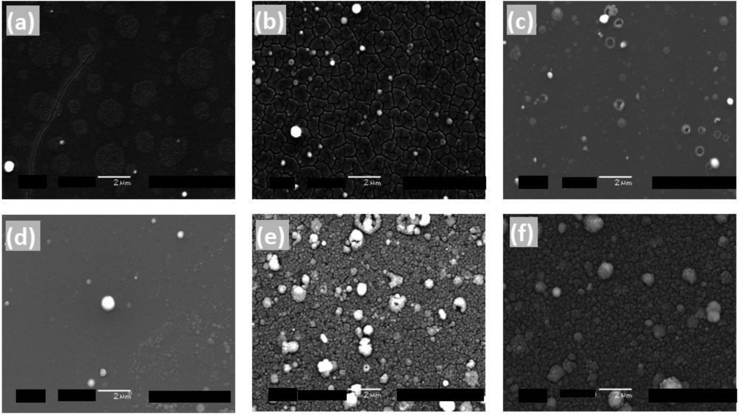
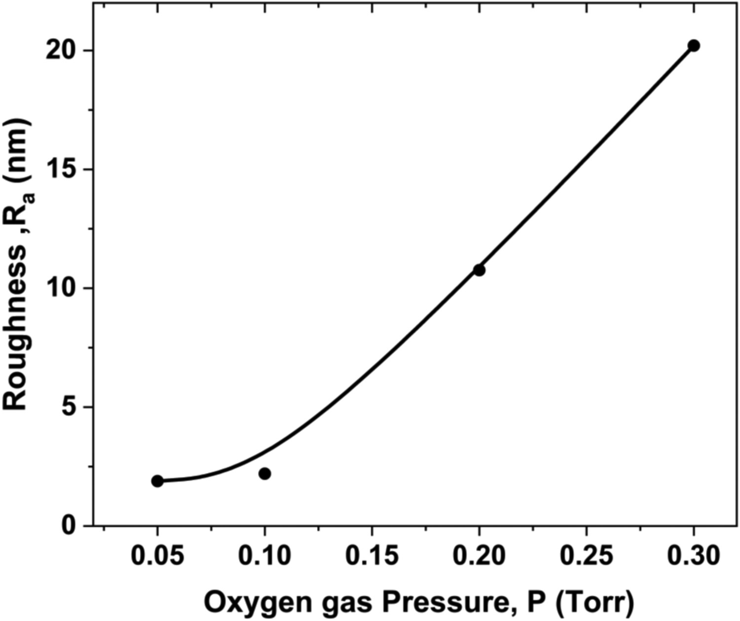
Figure 2 shows the AFM in three dimensions representations, for the NiO films that were deposited at different oxygen background pressures and two laser powers, namely 410 and 820 mW. The surface roughness deduced from the AFM images for both laser powers illustrates that the surface roughness is depending on the oxygen pressure during the deposition. The roughness is increasing from 1.18 nm to 20.8 nm as oxygen pressure during the deposition was increased from 0.05 to 0.3 Torr for samples that deposited at 410 mW laser power Figure 2(c–f). On the other hand, the NiO films that were grown at 820 mW showed not much changes in surface roughness as O2 pressure increases from 0.1 to 0.3 Torr, as shown in Figure 2(a,b). Figure 3 shows the increase in the average roughness, Ra of NiO films deposited on Si(100) substrate at vs. oxygen partial pressure during the PLD. The lower the oxygen pressure the smoother surface as well as the smaller the obtained grains in the films. The obtained results are in good agreement with results that were reported for reactive pulsed laser-deposited NiO films [10]. The increase in the surface roughness of the films with increasing oxygen background pressure is anticipated as the outcome of competition between the flux of atoms in the plume and the surface diffusion of the adatoms. The change in the gas pressure is absolutely affecting the adatom flux and the nucleation density. The surface roughness and the size of the formed grain in the deposited thin film are oxygen pressure dependents [19]. The higher the gas pressure, the lower the kinetic energy of adatom which leads to higher surface roughness and vice versa. The higher the gas pressure, the lower the kinetic energy of adatom which is leading to higher surface roughness and vice versa. The higher the kinetic energy of the adatoms, the smoother the surface of the NiO films, and certainly the kinetic energy of adatoms decreases with increasing pressure which lead to higher surface roughness at high pressure [19].
3D AFM recorded in tapping mode for NiO thin films deposited at different oxygen gas pressure, first two (a) 0.1 Torr, (b) 0.3 Torr at 820 mW and (c) 0.05 Torr, (d) 0.1 Torr, (e) 0.2 Torr, (f) 0.3 Torr at 410 mW. The average roughness, Ra Vs oxygen partial pressure during the deposition.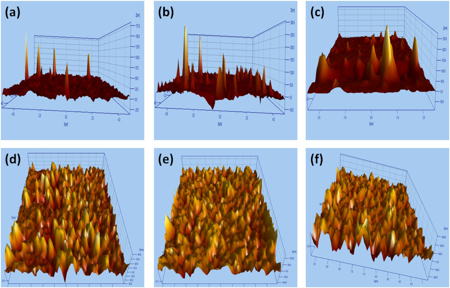
On the other hand, increasing the laser power at the same oxygen gas pressure results in less surface roughness of the NiO films as can be seen from both SEM and AFM images in Figure 1 and Figure 2(a,b) at 820 mW and (d,f) at 410 mW, respectively. The increase in the laser power causes an increase in the smoothness of the films’ surface as expected.
Increasing the laser power results in higher kinetic energy and a high flux of the ions of the plume [23]. Such results permit the formation of smoother NiO films, with low surface roughness, as seen in Figures 1 and 2.
EDX and photo spectral results
The conditions under which this series of samples were prepared, Ni and O atomic % and average surface roughness, Ra from AFM measurements.
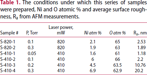
Figure 4 compares the results of the spectrums of Ni deposited under ultrahigh vacuum∼2 × 10⁻⁸ Torr with those of NiO deposited at 0.1 Torr at two different laser powers (410 and 820 mW). As shown in Figure 4 there are some extra peaks in the spectrum of the plume species at 0.1 Torr compared to the spectra of the plume obtained from the Ni target in ultrahigh vacuum conditions. The peak for oxygen O is developed specifically the strongest one at 777 nm. This is a confirmation of the reactive reaction of the laser with oxygen at the used oxygen pressure (0.1 Torr) and laser powers.
The photo spectra of Ni plume under high vacuum and at 0.1 Torr oxygen gas pressure for two laser powers 410 mW and 820 m.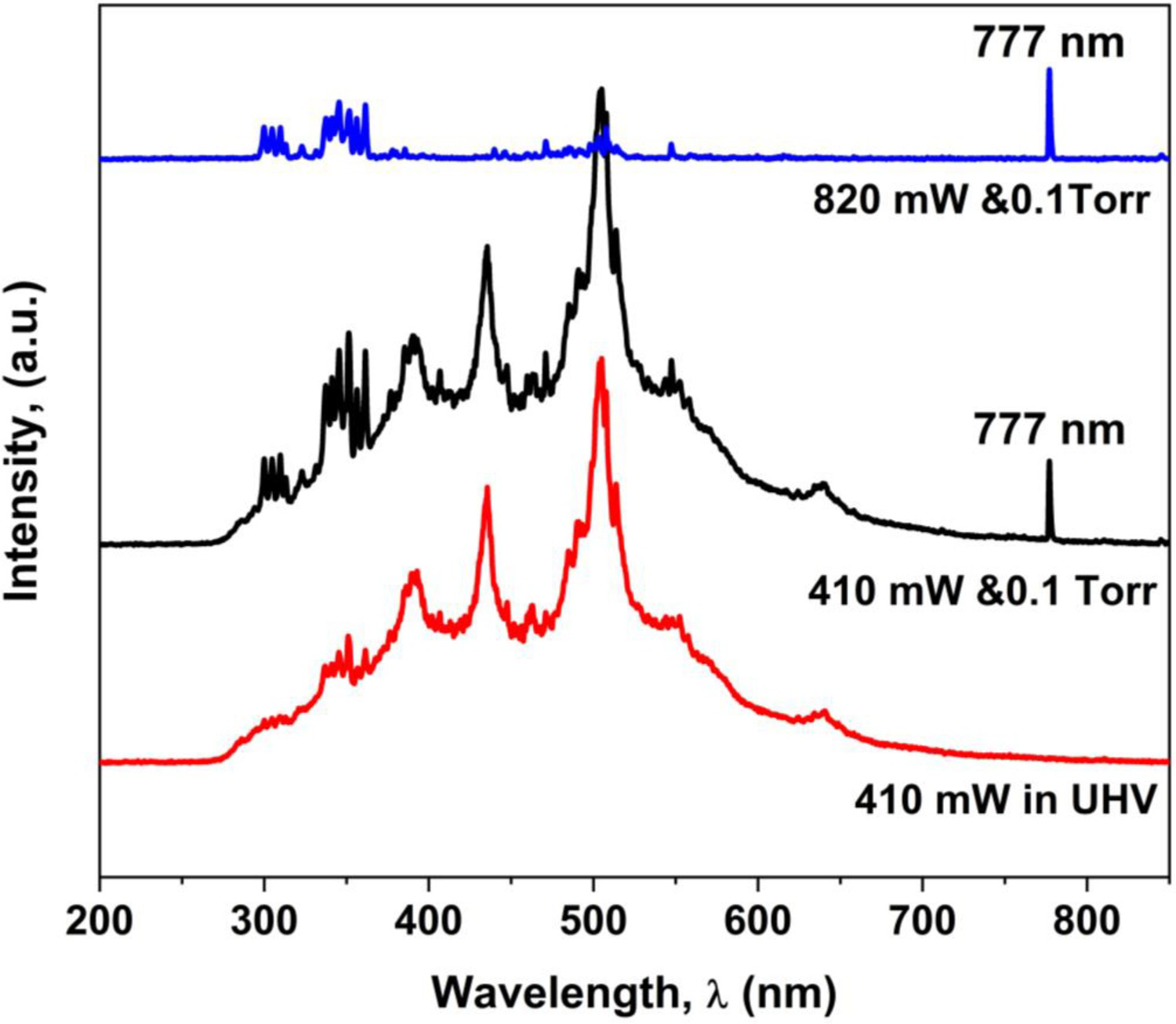
These results confirm that the selected gas pressure of 0.1 Torr results in NiO plume form NiO near stoichiometry uniform thin film.
Structural and morphological characterisation NiO films deposited at 0.1 Torr
The microstructures of NiO thin films deposited at 0.1 Torr were characterised by X-ray diffraction (XRD). Figure 5 shows XRD patterns of NiO thin films that were deposited on Si substrate at two laser powers (410 and 820 mW) and different substrate temperatures. As shown in Figure 5, the NiO films are not highly crystalline and the films have some preferred orientations that depend on laser power and on the substrate temperature. At a laser power of 410 mW, the preferred orientation of the cubic NiO structure is changing from (200) to (220) for NiO films with changes in the average crystallite size, D, from ∼27 nm to ∼9 nm, as temperatures of the substrate were increased from 200°C to 300°C. The average crystallite size was calculated from line broadening by X-ray diffraction using the Scherrer equation. On the other hand, as the laser power increases from 410 to 820 mW preferred orientation changes from (200) to (111) and D drops from 27 nm to 10 nm.
XRD diffraction patterns of NiO films deposited on Si(100) substrate at two different laser powers (410 and 820 mW) and two different substrate temperatures (200°C and 300°C).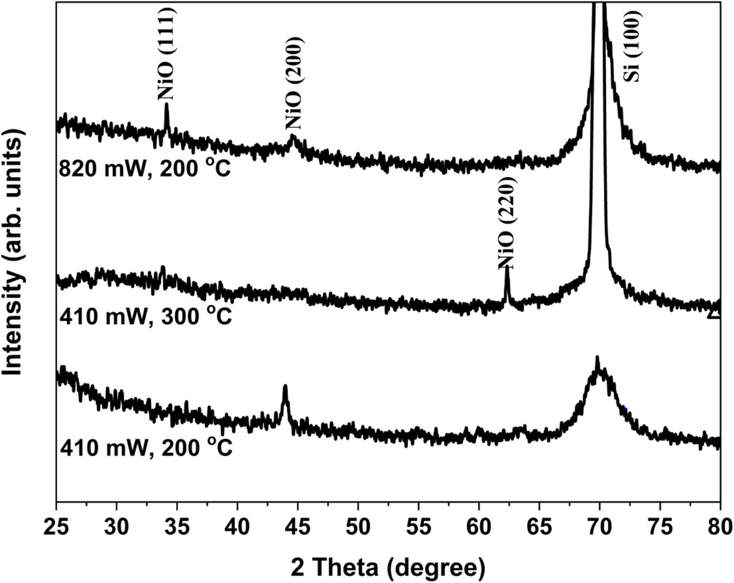
As the laser power is increasing the flux of Ni ions and the kinetic energy of the ablated plume are increasing [23]. This effect results in more dissociation and ionisation of oxygen which leads to increase oxygen content and this is extensively affecting the crystal structure of the film.
Here it is worth mentioning that several NiO samples were prepared at different oxygen gas pressure and two different laser powers to find out the paramount conditions of oxygen gas pressure to obtain good-quality NiO thin films with optimised optical band gap and lowest surface roughness. The best conditions were used to study the effect of laser power and annealing treatments on structural and surface morphology.
Based on previous results of surface roughness, EDX and photo spectra of Ni plumes the principal conditions for obtaining high-quality NiO thin films with the lowest surface roughness for oxygen gas pressure. The best conditions are for NiO films that were papered at an oxygen pressure of 0.1 Torr and 410 mW laser power.
Figure 6 shows the XRD of as-deposited NiO films grown on glass substrate at the preferred conditions: 0.1 Torr, 200°C and 410 mW. The results show that the sample is in an amorphous state embedded with NiO crystallites as indicated by the obtained hump at low 2-theta angles and crystalline NiO cubic peaks at (101), (111) and (220), as shown in Figure 6. As the sample was annealed at 300°C for 2 h under N2 gas flow the intensities of that peak are increasing with a preferential orientation in (111) direction. As the annealing time extended to 8 h the NiO peaks became dominant in the amorphous phase. The intensity of the (111) peak is increasing relative to the intensities of the other two peaks and then the preferential orientation is the (111) direction. The increase in the intensity of the XRD with an increase of annealing temperature and annealing time could be due to the improvement of the surface oxidation of the film which is reflecting progress in the crystallinity and that causes re-crystallisation of the film [24].
XRD diffraction patterns of NiO films deposited on glass substrate annealed at 300°C for two different periods.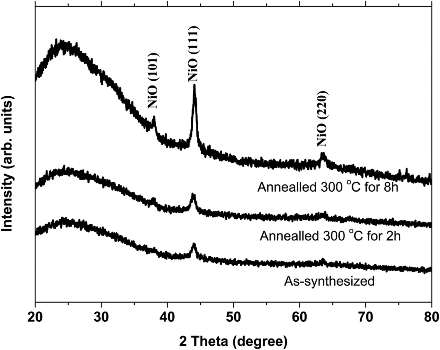
Figure 7 shows the TEM image of the NiO thin films deposited at 0.1 Torr and two different laser powers 410 and 820 mW. One can see that the NiO nanostructures were formed on the film with size decreasing as laser power was increasing. The insets in Figure 7(a,b) show the SAED patterns of NiO nanostructures formed in the films. The formation of such rings indicated the formation of NiO in the cubic phase. The obtained rings of the SAED pattern cloud be indexed from inside to outside as the (111), (200), (220), and (311) reflections of the NiO cubic phase [8]. Figure 7(b,d) show high magnification images of NiO films grown on Cu- grids at 0.1 Torr at two different laser powers 410 and 820 mW. The investigation of these TEM images shows that the formation of nanoparticles on the film same as in the SAED patterns. Such results confirm the formation of poly-crystal NiO thin films which are in agreement with the XRD results. On the other hand, the structure of the obtained NiO thin films here is different from the structure obtained from XRD results. Since for TEM measurements Cu- grids were used as a substrate and which is different from the XRD case. The degree of mismatch between the thin film and substrate structures is deeply affecting the structure of the grown thin film.
HRTEM of NiO/Si at 0.1 Torr (a) and (b) at 410 mW (c) and (D) at 820 mW.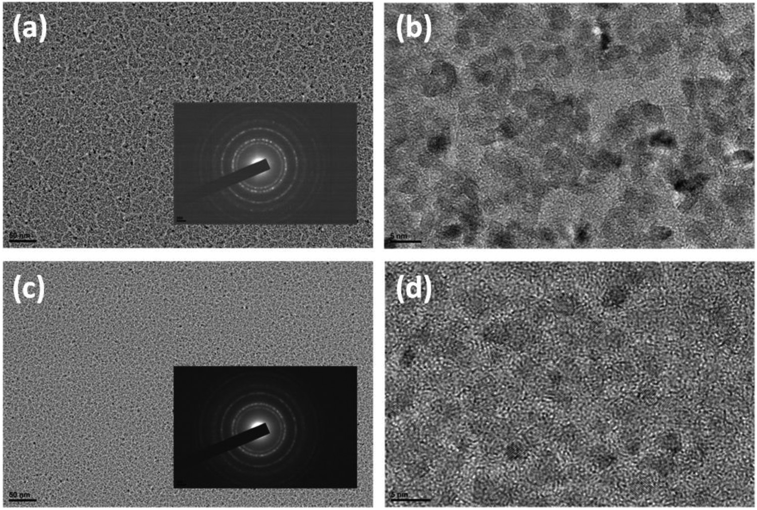
Figure 8 shows the surface morphological images of NiO films deposited at different laser powers using the AFM technique. AFM images were obtained for films in the air by tapping mode. NiO film that was deposited at 410 m W laser power showed nanoparticles with an average particle size of 42–46 nm with some smaller nanoparticles. As the laser power was increased to 820 m W the obtained NiO film cosseted smaller sizes of the NiO nanoparticles. The average particle size for the sample that was prepared at 820 m W laser power was 23–26 nm. Such smaller particle size leads to a much smoother surface. Increasing the laser power results in more ions with higher kinetic energy in the laser plume which is ensuing lower surface roughness. This is good agreement with a previous study that was using reactive PLD, that higher laser power results in in smaller particles size [23]. The higher the laser power, the lower the size of formed nanoparticles which confirmed the TEM results of NiO films in Figure 7.
2D AFM images of NiO/Si at 0.1 Torr (a) at 820 m and (b) at 410 mW.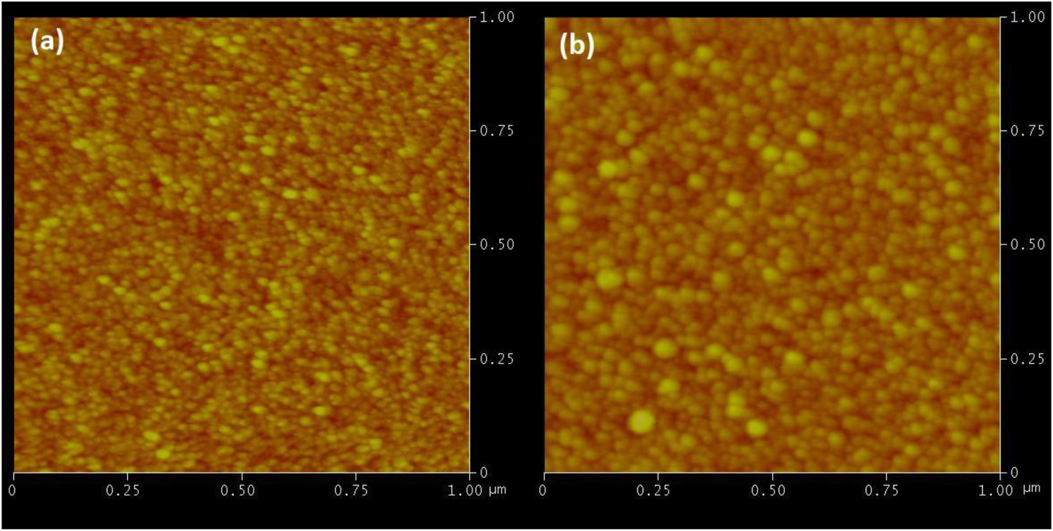
Optical properties niO film deposited at 0.1 Torr
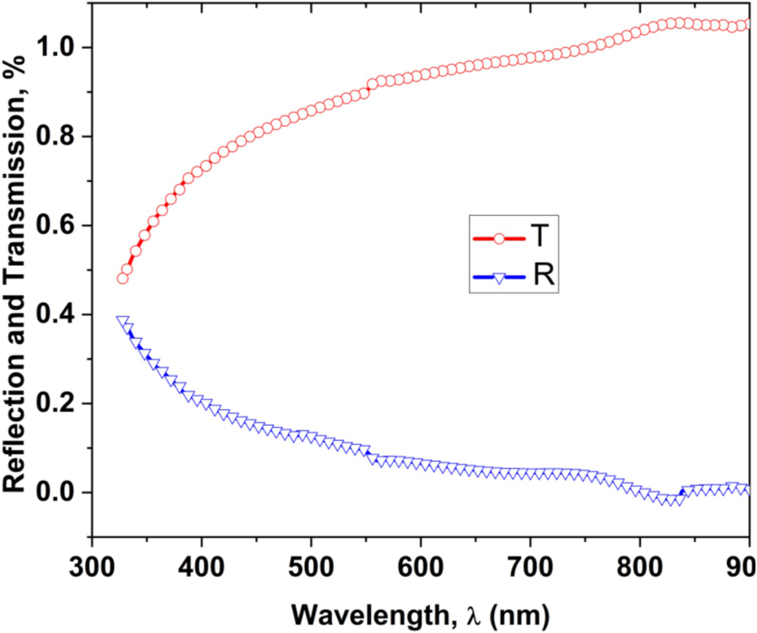
Figure 9 shows the optical transmittance and reflectance spectra of NiO film that was deposited on glass substrate at 0.1 Torr and 200°C in the wavelength range 190–900 nm. The NiO film illustrates high transparency over a higher region of the wavelength then the transmission of the film drops in the shorter wavelength range, as seen in Figure 9. The optical parameters of the film that are including refractive index (n), absorption coefficient (α) and energy gap (Eg) were determined. The refractive index (n) was calculated from the reflectance data (R = 1-T-A) according to the following equation [25]:
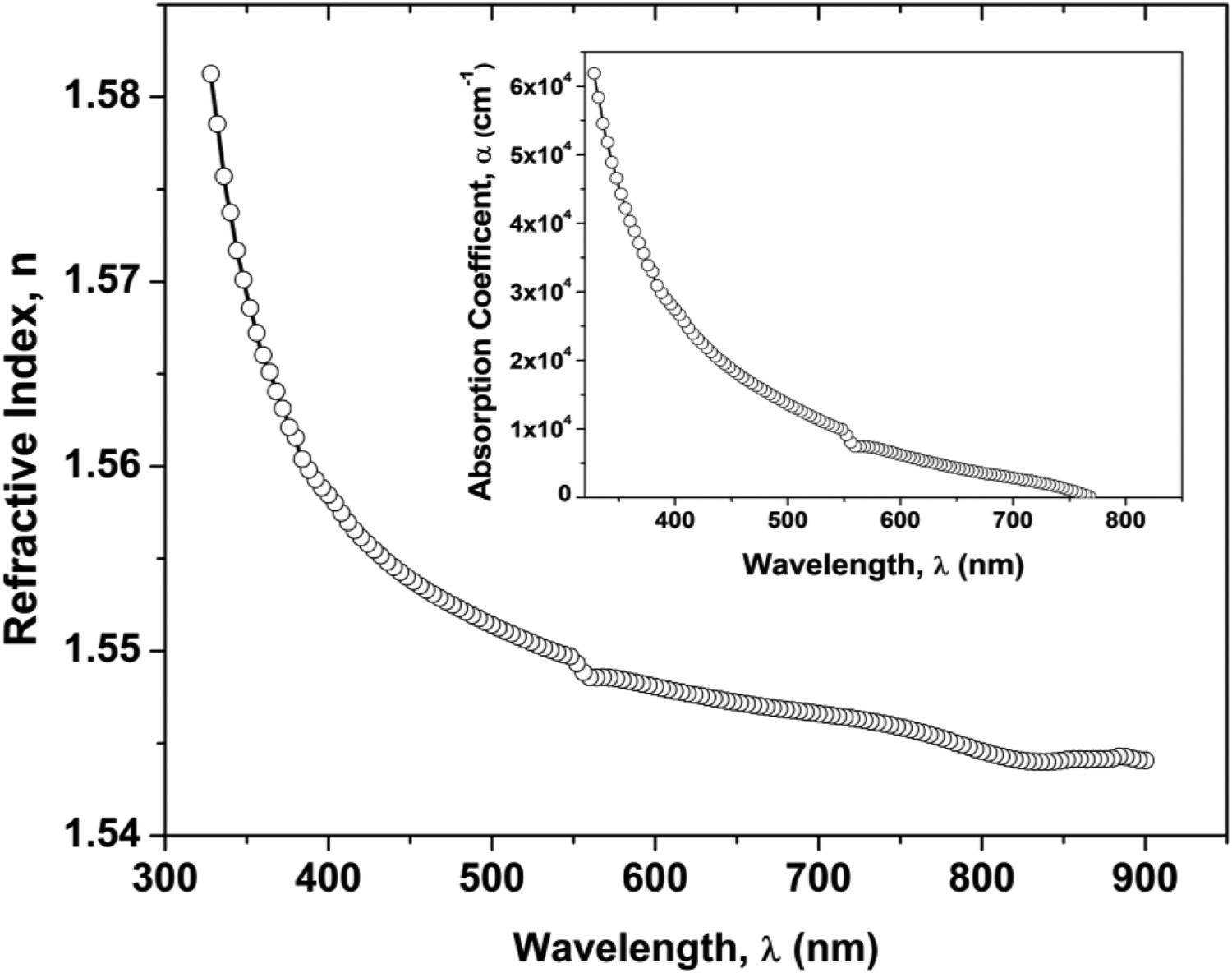
Spectral variation of transmittance T and reflectance of NiO film deposited on glass substrate at 0.1 Torr and 200°C in the wavelength range 190 to 900 nm. The refractive index, n vs. the wavelength of NiO film deposited on glass substrate at 0.1 Torr and 200°C. The inset shows the variation of absorption coefficient α vs. the wavelength.


The optical band gap of the NiO film had been calculated from the Tauc equation for direct-band gap materials [30]:
The variation of 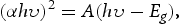
Conclusion
NiO thin films were deposited from metallic Ni targets at different oxygen gas pressures using the reactive PLD technique. The changes in two of the PLD parameters, namely, the laser power and oxygen gas pressure, were employed to reach the best optimal conditions to grow NiO films on both glass and Si(100) substrates. NiO thin films crystallised in a cubic NiO structure with particle size that depends on laser power as seen from SEM and AFM results. The oxygen partial pressure during the deposition significantly affects the chemical composition and the surface morphology of NiO films. The paramount conditions to obtain good-quality NiO film is an oxygen pressure of 0.1 Torr and 410 mW laser power. Annealing of NiO deposited on glass substrate at 300°C under N2 gas flow showed a preferential orientation dominated in the (111) direction due to the improvement of the oxidation of the film. The optical band gap of NiO film deposited at 0.1 Torr was 3.35 eV. The preferred orientation changed from (200) to (111) and crystallite size dropped from 27 to 10 nm and average particles size decreased from 46 to 26 nm as laser power was increased from 410 mW to 820 mW of the NiO films on Si(100) substrate at 200°C and 0.1 Torr.
Footnotes
Disclosure statement
No potential conflict of interest was reported by the author(s).