






Abstract
TiN x films were deposited using direct current reactive magnetron sputtering on glass substrates, and the variation of resistivity and infrared emissivity of TiN x films deposited at different substrate temperatures was investigated. The N/Ti ratios of prepared films were off-stoichiometric, and reached the highest value 0.97 at 350°C. The results showed that substrate temperature had an important role in regulating the resistivity and infrared emissivity of TiN x films, and the change in resistivity of the films was consistent with their infrared emissivity. As the substrate temperature increased from 25 to 350°C, the resistivity of the films decreased from 15.7 × 10³ to 0.9 × 10³ μΩ cm. Infrared emissivity in the wavelength of 3–5 μm decreased from 0.55 to 0.29, and the value in the wavelength of 8–14 μm dropped from 0.54 to 0.27.
Introduction
With the rapid development of infrared technologies, low infrared emissivity materials attract more and more attentions due to their widespread applications in civil and military fields, such as energy conservation in industry field and military targets stealth or infrared detection in the military field [1,2]. As a consequence, various new materials with low infrared emissivity have been prepared and investigated to satisfy the applications of different infrared technology fields [3-5].
Titanium nitride (TiN) film exhibits a unique combination of physical and chemical properties, including exceptional hardness, high resistance to wear and corrosion, high thermal stability and good electrical conductivity. Therefore, TiN film has been widely used in many industrial areas, such as hardening coatings on tools, decorative coatings, the diffusion barriers and adhesive layers for electronic devices etc. [6-10]. As an attractive transition metal nitride, TiN exhibits free-electron-like behaviour and good electrical conductivity [11]. During the formation of TiN, each N atom with five valence electrons in the outer shell, gives them away to form chemical bonds with its nearest neighbours. Each Ti atom with four valence electrons in the outer shell, gives three electrons away to form covalent bonds with nitrogen (Ti–N), and the fourth valence electron is redundant [12]. These redundant electrons produce shallow donor levels in the band gap of TiN, and can be easily activated into the conduction band [13]. Therefore, the interaction between the free carrier of TiN film and the infrared electromagnetic wave is similar to that of the metal, indicating that TiN film may have a low infrared emissivity and is promising for infrared applications. However, there is a lack of systemic studies that explore the infrared properties of TiN film.
DC reactive magnetron sputtering is of importance in the industrial production of TiN films, which provides TiN films with various properties by altering the technique parameters such as substrate temperature [14-16]. In this study, TiN x films were deposited onto the heated substrates using DC reactive magnetron sputtering, and the structure, electrical properties and infrared emissivity of TiN x films at different substrate temperatures were discussed.
Experiments
Deposition of TiN x films
The deposition of TiN x films was carried out on glass substrates with a Ti target (99.995% in purity) using a direct current reactive magnetron sputtering system (JPG450). The base pressure of vacuum chamber was pumped to 5.0 × 10 −4 Pa. Before deposition, the target was pre-sputtered by Ar gas (99.999% in purity) for 15 min to remove the surface oxide layer. After pre-sputtering, the mixture of Ar and N2 gas (99.999% in purity), fixed at 100 and 20 standard cubic centimetres, respectively, was introduced into the chamber using mass flow controllers to regulate the flow of gas. A total gas pressure of 0.6 Pa and a sputtering power of 120 W were used to deposit 400 nm films. During the film deposition, the substrate temperatures for different samples were held at 25, 150, 250 and 350°C, respectively.
Characterisation techniques
The crystal structure and grain size of TiN x films were obtained by an X-ray diffraction analysis (Philips X'Pert Diffractometer). Cu Kα (λ = 0.1514 nm) radiation was used as the source for diffraction. The bonding states of elements and N/Ti ratios of the films were identified by X-ray photoelectron spectrometry (XPS, ESCALAB 250Xi). Composition analysis was performed after ion etching 360 s using 3KeV Ar+. The thickness was observed by a field-emission-gun scanning electron microscopy (ZEISS SUPRA 55). The resistivity of the films was measured with a standard four-point probe measurement method. The carrier concentration and Hall mobility were measured by a Hall measurement system. The infrared emissivity of TiN x films in the wavelength of 3–5 and 8–14 μm was measured using an ISTP IR-2 dual-band emissivity tester at room temperature.
Results and discussion
Phase constituent of TiN x films
The XRD patterns of TiN
x
films deposited at different substrate temperatures are shown in Figure 1. It confirms that all the films are composed of TiN phase with a faced-centered cubic crystal structure based on JCPDS No.87-0628. An obvious (200) peak is observed for all the films, indicating that TiN
x
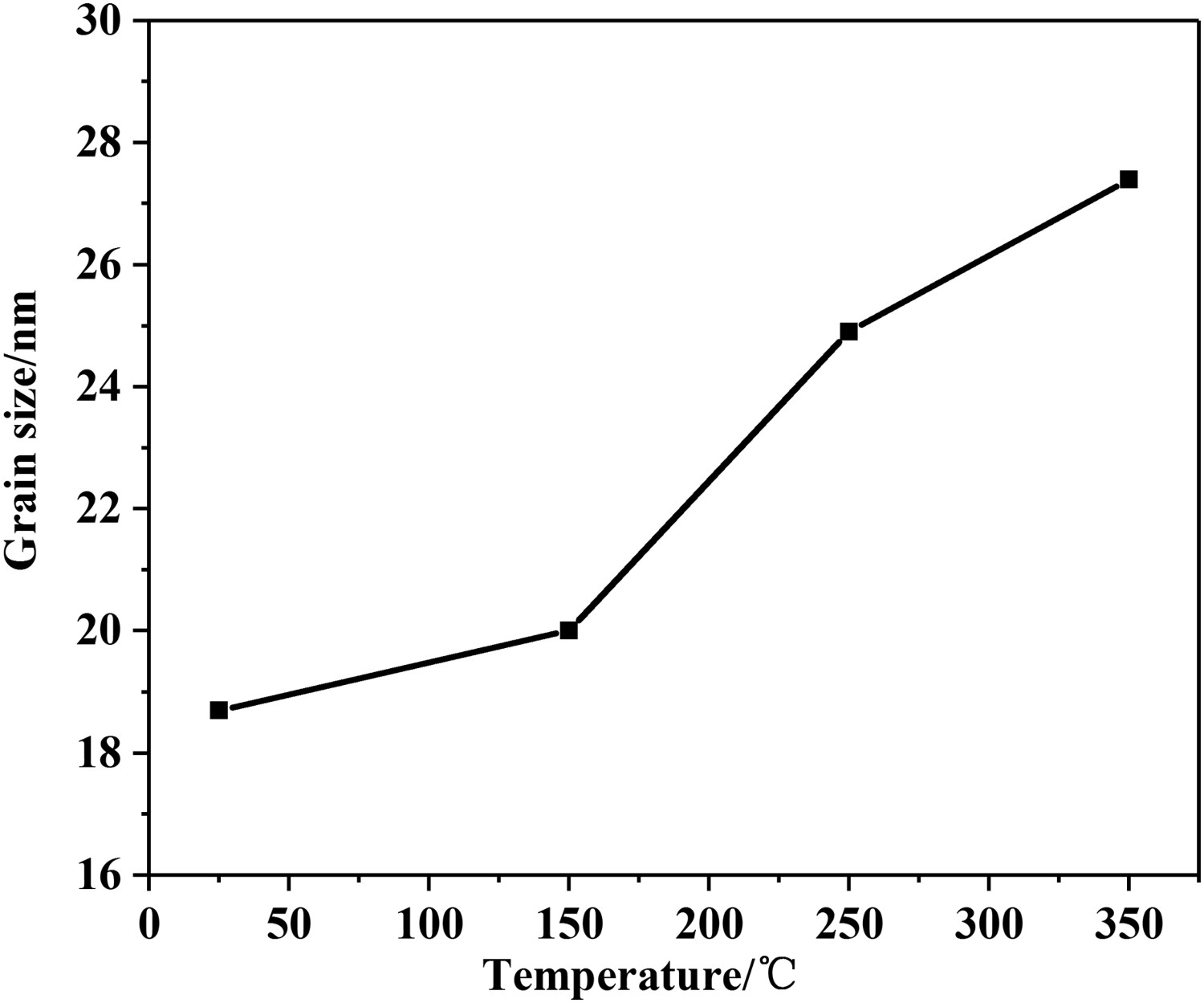
films with polycrystalline structure are formed. It can be observed that the (111) and (220) crystalline plane is negligible for the films except for the film deposited at 250°C, which exhibits a mixture of the structure in a more pronounced (200) orientation with less (111) and (220), showing changes in the crystalline orientations. As substrate temperature increases, the intensity of XRD peaks also increases and the full width at half maxima of the peaks becomes narrower, indicating a rise in grain size. The grain sizes of TiN
x
films deposited at different substrate temperatures are shown in Figure 2. The grain size (D) of TiN
x
films can be calculated using the Scherrer equation [17]:
XRD patterns of TiN
x
films deposited at various substrate temperatures. Grain sizes of TiN
x
films deposited at various substrate temperatures.

Binding states of the elements in TiN x films
The X-ray photoelectron spectra of Ti 2p and N 1s for TiN
x
film deposited at 250°C are shown in Figure 3(a,b). The binding energies of the peaks are calibrated respect to C 1s peak at 284.8 eV. In Figure 3(a), Ti 2p states exhibit 5 binding peaks, which are 454.9, 456.2, 457.8 eV of Ti 2p3/2 and 460.9, 463.0 eV of Ti 2p1/2. The XPS peak of Ti2 p3/2 at 454.9 eV can be ascribed to the formation of TiN phase [18,19]. The peaks at 456.2 eV and 457.8 eV suggest the formation of the titanium oxy-nitride and TiO2 phase. The peaks of Ti 2p1/2 are composed of two peaks at 460.9 eV (TiN) and 463.0 eV (TiO2). In Figure 3(b), the peaks of N 1s spectra at 397.3 eV and 399.5 eV can be assigned to the presence of TiN and titanium oxy-nitride phase, respectively, [20,21].
XPS spectra of TiN
x
films deposited at 250°C (a) Ti 2p; (b) N 1s.
The N/Ti ratios calculated from the XPS spectra of the films are shown in Figure 4. The N/Ti ratio rises when the substrate temperature increases, whereas the ratio of N/Ti at 250°C is exception. The N/Ti ratio is in range of 0.81–0.97, indicating that all the films are off stoichiometry and deficit in nitrogen. When the substrate temperature increases, the mobility and diffusion of reactive atoms are enhanced to reduce the detrimental effects and increase the N/Ti ratio. At 250°C, the N/Ti ratio shows a sudden decrease, which could be explained by the orientation of TiN
x
films. Combadiere et al. [22] reported that the (111) planes consisted only of Ti atoms. As for the (220) and (200) planes, they contained both N and Ti atoms. The film deposited at 250°C exhibits an obvious (111) plane, so there are more Ti atoms in the film deposited at 250°C than others, which leads to the sudden decrease of the N/Ti ratio. This result is in good agreement with those obtained by XRD.
N/Ti ratios of TiNx films deposited at various substrate temperatures.
Electrical properties of TiN x films
Figure 5(a,b) shows the resistivity, carrier concentration and Hall mobility of TiN
x
films deposited at different substrate temperatures. It is observed that the substrate temperature has a significant effect on the electrical properties of TiN
x
films. The resistivity of TiN
x
films decreases obviously from 15.7 × 10³ μΩ cm at 25°C to 0.9 × 10³ μΩ cm at 350°C. It is known that the non-stoichiometric TiN
x
films contain more lattice defects, which increase the resistivity of the films. Therefore, the resistivity of TiN
x
films is higher than the single-crystal TiN film, 18 µΩ cm [23].
Electrical properties of TiN
x
films deposited at various substrate temperatures (a) Resistivity; (b) Carrier concentration and Hall mobility.
The evolution of resistivity can be explained by the changes of carrier concentration and Hall mobility using Equation (2) [24]:

When the substrate temperature goes up, the N/Ti ratio of TiN x film is closer to the stoichiometric ratio, as shown in Figure 5(b), the carrier concentration n increases. Meanwhile, with substrate temperature increase, the grain size of TiN x films rises and the crystal structure of films grows more perfect, causing that the number of grain boundary and crystalline defects decreases. The structure of TiN x films becomes denser, leading to an increase of mobility μ due to the decrement of grain boundary scattering and crystalline defects scattering. Consequently, the resistivity of TiN x film goes down.
Infrared emissivity of TiN x films
The infrared emissivity curves in the wavelength of 3–5 and 8–14 μm of TiN
x
films deposited at various substrate temperatures are shown in Figure 6. The increase in substrate temperature leads to the decrease of infrared emissivity of the films. With the substrate temperature rising from 25 to 350°C, the infrared emissivity of TiN
x
films in the wavelength of 3–5 μm decreases from 0.55 to 0.29, and the value in the wavelength of 8–14 μm drops from 0.54 to 0.27. The change in infrared emissivity of the films is consistent with their resistivity, which can be explained using the Hagen-Rubens equation [25]. According to Hagen-Rubens relation, the infrared emissivity ε can be expressed as Equation (3).
Infrared emissivity of TiN
x
films deposited at various substrate temperatures.

Conclusions
TiN x films were prepared on glass substrates using DC reactive magnetron sputtering technique, and the variation of resistivity and infrared emissivity of TiN x films deposited at different substrate temperatures (25, 150, 250 and 350°C) was investigated. The XRD patterns revealed that the prepared films were composed of TiN phase with the (200) preferred orientation, and the grain size along the sample surface went up with the substrate temperature rise. The prepared films were off-stoichiometric, and N/Ti ratio reached the highest value 0.97 at 350°C. As the substrate temperature rose from 25 to 350°C, the resistivity of the films decreased from 15.7 × 10³ to 0.9 × 10³ μΩ cm. Infrared emissivity of TiN x films in the wavelength of 3–5 μm decreased from 0.55 to 0.29, and the value in the wavelength of 8–14 μm dropped from 0.54 to 0.27. Increase in the substrate temperature had an important role in regulating the resistivity and infrared emissivity of TiN x films, suggesting that TiN x film is promising for infrared applications.
Footnotes
Disclosure statement
No potential conflict of interest was reported by the authors.