
Abstract
Li-doped CdS (CdS:Li) thin films with 0, 1, 2 and 3 wt-% Li concentrations were prepared by the spray technique using a perfume atomiser. The effect of Li doping concentration on the structural, optical, electrical and magnetic properties was systematically investigated and the results are reported in this paper. Analysis of the microstructure indicates that all the films consist of a hexagonal CdS phase with a strong (0 0 2) preferential growth texture. Nanoneedles were evinced from the SEM images of the doped films. Optical studies reveal that the transparency and band gap were dependent on Li-doping content. Hall effect measurements reveal that all the doped films exhibit p-type conductivity and the resistivity values strongly depend on the occupancy of Li atoms on the substitutional and interstitial sites of the CdS lattice. Room temperature ferromagnetism was observed for the doped films.
Introduction
Cadmium sulphide (CdS) is a promising II–VI group n-type semiconductor that possesses special optoelectronic properties, moderate band gap (2.42 eV) and excellent stability which makes it suitable for solar cell applications as an efficient window layer, photo anodes in photo-electrochemical solar cells, tuneable light-emitting diodes, etc. [1,2]. Nanostructured CdS functionalised with bio-molecules finds applications in biology as a molecular fluorescent probe [3]. The performance of CdS-based devices depends on its structural, optical and electrical properties which can be controlled by adjusting its native defects such as cadmium interstitials/sulphur vacancies through doping. It has been reported earlier that monovalent atoms can effectively control the native defects of CdS, thereby making it suitable for various applications [4,5]. Improved photosensitive properties of CdS through boron doping have been reported by Challa et al. [6]. Decreased electrical resistivity and increased transparency have been reported for Ag-doped CdS thin films by Narasimman et al. [7]. High optical transparency and decreased resistivity have been reported for CdS thin films doped with chloride by Sivaraman et al. [8]. Improved optical and electrical properties of CdS thin films through bromine doping have been reported by Narasimman et al. [9]. Lithium is a monovalent atom which proved to be effective in improving the electrical properties of NiO thin films [10]. Improved electrical conductivity through Li doping has been reported by Dakhel et al. [11] for CdO thin films. Among the group I elements, Li has the shallowest ionisation energy which can modify the optical, electrical and ferroelectric properties of semiconductor oxide thin films [12,13]. Improved ferromagnetism through indirect exchange via Li-related defects has been reported by Lin et al. [14] for Co, Li-codoped ZnO thin films. Motivated by these observations, it can be predicted that Li doping could enhance significantly the structural, optical, electrical and magnetic properties of CdS thin films. Hence, in this work, Li-doped CdS thin films with 0, 1, 2 and 3 wt-% Li concentrations were deposited by the spray technique using a perfume atomiser and the effect of Li doping on the structural, optical, electrical and magnetic properties of CdS thin films was systematically investigated and reported. The spray technique using a perfume atomiser is used to deposit the undoped and Li-doped CdS thin films. The use of perfume atomiser has several advantages such as low cost and lesser deposition temperature. [15].
Experimental details
Li-doped CdS (CdS:Li) thin films were prepared by the spray technique using a perfume atomiser. Cadmium chloride [CdCl2·2H2O], thiourea [SC(NH2)2] and lithium chloride [LiCl3·2H2O] were used as the precursor salts to deposit CdS:Li thin films. Aqueous solution (40 mL) of cadmium chloride and thiourea, each of 0.05 M was sprayed over hot glass substrates to get CdS thin films. To achieve lithium doping, lithium chloride with concentrations 1, 2 and 3 wt-% was added to the above-prepared solution and sprayed. The thickness values of the films measured using a stylus profilometer (Surftest SJ-301) were found to be equal to 393, 418, 411 and 406 nm, respectively, for the CdS film doped with 0, 1, 2 and 3 wt-% Li-doping concentrations. The crystal structure of the CdS:Li thin films was studied using a X-ray diffractometer (X-pert PROanalytical-PW340/60) with CuKα radiation (λ = 1.5406 Å). Surface morphology of the films was analysed using a scanning electron microscope (HITACHI S-3000H) and a transmission electron microscope (200 KV Technai-20G2). Transmission spectra were recorded using UV–VIS-NIR double beam spectrophotometer (LAMBDA-35). Electrical studies were performed using the Hall measurement set-up. Magnetic studies were performed using a vibrating sample magnetometer (Lakeshore 7410).
Results and discussion
XRD analysis
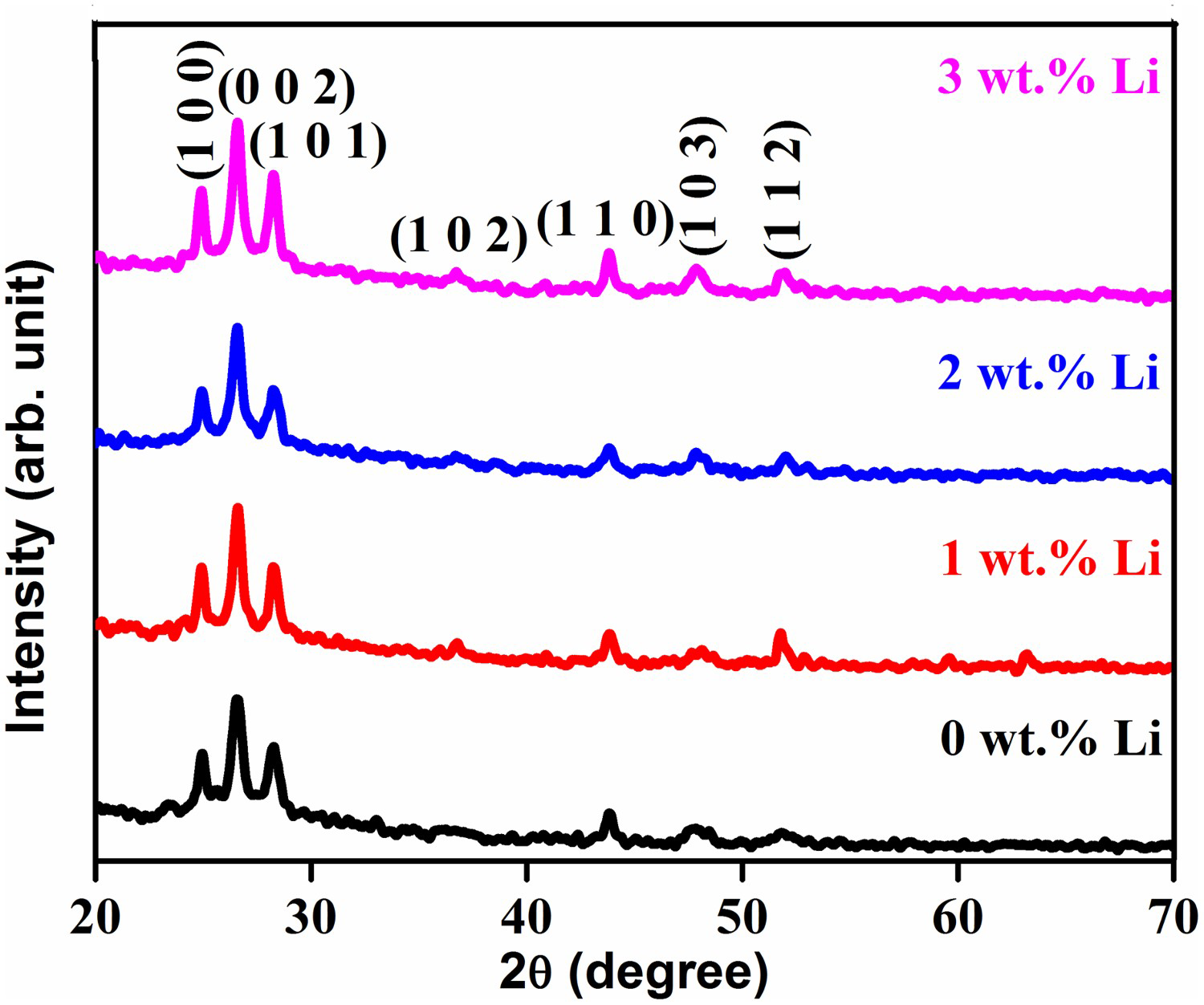
Figure 1 shows the X-ray diffraction spectra of the CdS:Li thin films. Well-defined diffraction peaks associated with the hexagonal phase of CdS (JCPDS Card No. 65-3414) were observed in the spectra. It is clear that the growth of the CdS:Li thin films occurs in the (0 0 2) direction normal to the plane of the films. Similar (0 0 2) preferential growth has been reported earlier in the literature [9,16]. No traces of Li-related phases were observed within the sensitivity of XRD measurements. The variation of the peak position (2θ), full width at half maximum (FWHM) (β), d-spacing value of the (0 0 2) plane, lattice parameters ‘a’ and ‘c’, particle size (D) and strain (ε) values of the CdS:Li thin films are compiled in Table 1. The peak position slightly shifts towards higher (2θ) angle up to 1 wt-% of Li, suggesting lattice contraction, which might be due to the decrease in interatomic spacing due to the substitution of smaller sized Li+ ions (0.68 Å) into the CdS lattice replacing larger sized Cd2+ ions (0.97 Å). The peak positions of the 2 and 3 wt-% Li-doped films shift towards lower (2θ) angles which are related to the increase of their lattice constant values which might be due to the limited solubility of Li in CdS and the extra Li atoms may be incorporated at the interstitial sites of the CdS lattice leading to its expansion. This is in accordance with the results reported by Wang et al. [17] for Mg-doped SnS2 nanoflowers. The particle size (D) and strain (ε) values were calculated from the (0 0 2) plane using the following formulae:
XRD patterns of the CdS:Li thin films. 2θ, full width at half maximum (β), d-spacing, particle size (D), lattice constants, strain (ε) and electrical resistivity values of the CdS:Li thin films.

SEM and TEM studies
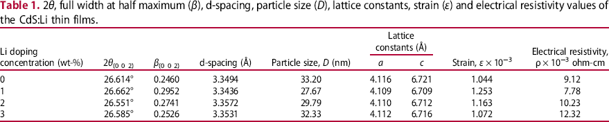
Figure 2 shows the SEM images of (a) 0 wt-%, (b) 1 wt-%, (c) 2 wt-% and (d) 3 wt-% Li-doped CdS thin films. Nanosized needle-shaped grains were observed for the doped films. Figure 3 shows the TEM images of (a) 0 wt-%, (b) 1 wt-%, (c) 2 wt-% and (d) 3 wt-% Li-doped CdS thin films. Grains appear to be in nanoregime for all the films. Even though, needle-shaped grains could not be detected in the TEM images, they can be observed from the SEM images that Li doping strongly influenced the surface morphology of pure CdS.
SEM images of (a) 1 wt-%, (b) 2 wt-%, (c) 3 wt-% and (d) 4 wt-% Li-doped CdS thin films. TEM images of (a) 1 wt-%, (b) 2 wt-%, (c) 3 wt-% and (d) 4 wt-% Li-doped CdS thin films.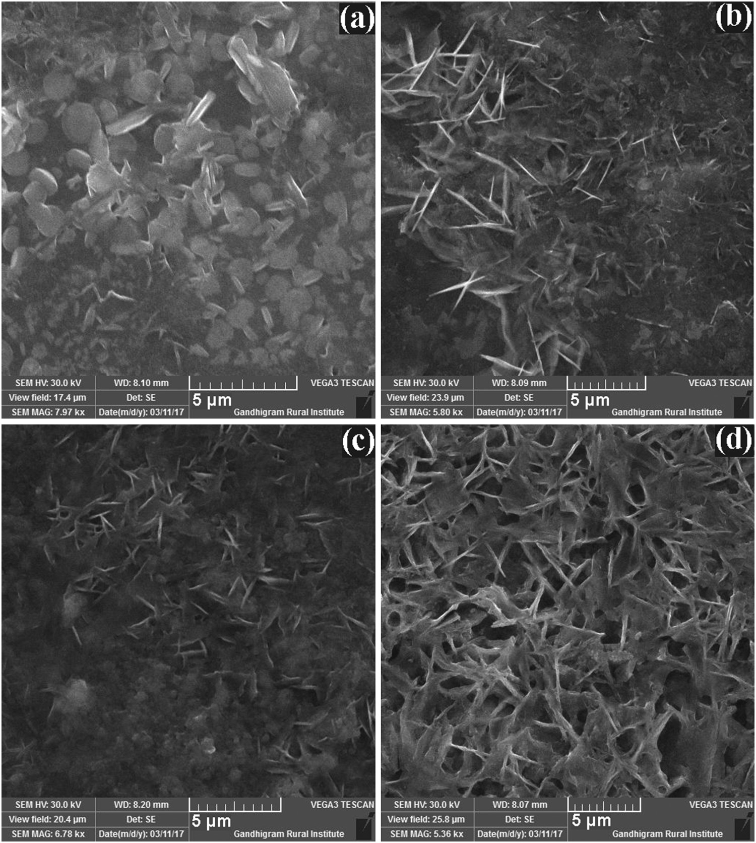
XPS studies
Figure 4(a) shows the survey scan spectrum of 1 wt-% Li-doped CdS thin film (film with better structural properties). Elements Cd, S and Li were observed in the spectrum. The high-resolution XPS spectrum of Cd3d shown in Figure 4(b) confirmed the presence of Cd3d5/2 peak at 403.8 eV and Cd3d3/2 peak at 410.6 eV with a spin-orbital splitting of 6.8 eV. The XPS spectrum of S2p (Figure 4(c)) observed at 160.4 eV corresponds to S2− in the CdS [19]. The Li 1s peak is observed around 38 eV.
XPS spectrum of the 1 wt-% Li-doped CdS thin film.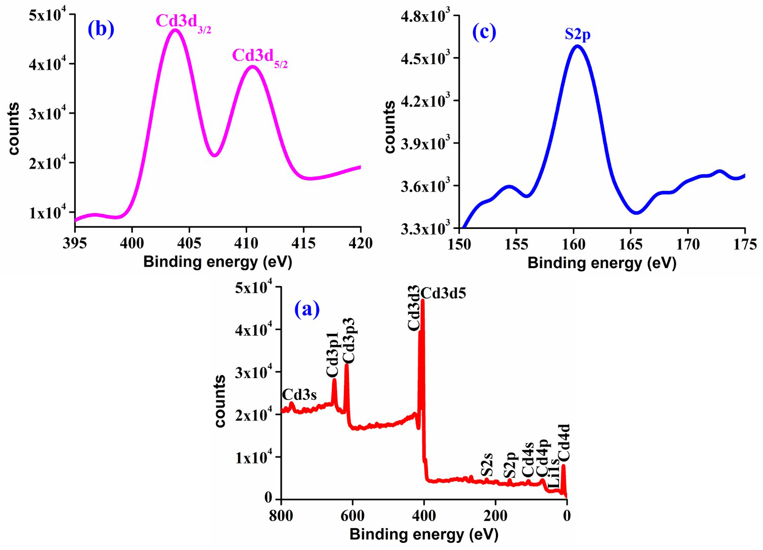
Optical studies
Lithium has one valence electron less than that of cadmium and hence substitutional incorporation of Li+ ions (Licd) in CdS can create one hole in sulphur p state, while the interstitial Li (Lii) can introduce one electron in the CdS lattice and hence in the CdS:Li system, Licd and Lii may exhibit both acceptor and donor behaviours, respectively. Figure 5(a) shows the optical transmittance spectra of the CdS:Li thin films. All the films exhibit a maximum transparency of nearly around 80%. To investigate the effect of dual nature of Li on the band gap (Eg) of the CdS thin films, UV–VIS-NIR absorption spectra of the films were recorded and from the relation between the absorption coefficient (α) and the incident photon energy (hν), the Eg values were calculated by extrapolating the linear portion of the (αhυ)2 vs. hυ plots (Figure 5(b)) to the energy axis at α = 0. The Eg value of pure CdS thin film is found to be equal to 2.3 eV, which is in agreement with an earlier reported value [20]. As Li-doping concentration increases from 0 to 1 wt-%, the Eg value decreases from 2.3 to 2.24 eV and it slightly increases to 2.35 and 2.42 eV, respectively, for the 3 and 4 wt-% Li-doped samples. Similar results have been reported by Etefagh et al. [21] for Zn-doped SnS2 thin films. The decrement in the Eg value observed up to 1 wt-% Li doping concentration might be due to the dominance of Licd which acts as acceptors. Licd produces acceptor band inside the forbidden gap region, thereby reducing Eg. The decrement in the band gap value observed for the 1 wt-% Li-doped sample might also be due to the formation of Li-related localised levels in the forbidden zone closer to the band maxima of conduction band as reported by Chelouche et al. [22] for Li, Ce co-doped ZnO thin films deposited by the sol–gel dip coating method. However, for the 2 and 3 wt-% Li-doped films, Licd reaches saturation transforming Licd into Lii which exhibits donor behaviour. Lii weakens the acceptor band, thereby slightly increasing Eg. The Fermi level inside the conduction band moves upwards with increasing donor concentration due to the filling of conduction band by the increase of electron carriers. Thus, more electrons occupy states at the bottom of the conduction band causing it to be filled up with donor electrons. So, electrons could not be excited from the valence band maximum to the minimum of the conduction band and hence higher energies are required to reach unoccupied states resulting in the widening of band gaps. Similar results have been reported by Mugwang'a et al. [23].
(a) Transmittance spectra and (b) Plots of (αhν)2 versus hν of the CdS:Li thin films.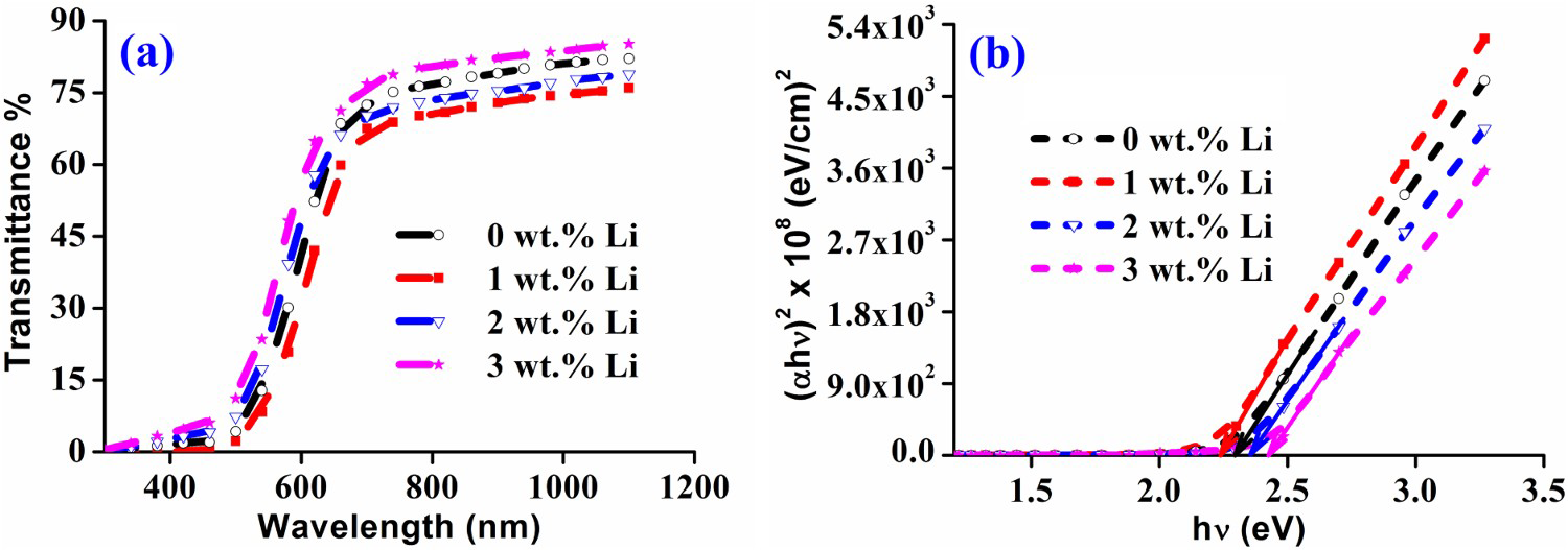
Electrical studies
The electrical properties of the undoped and Li-doped CdS thin films were measured at room temperature using the Hall effect measurement set-up (schematically shown in Figure 6). Undoped CdS films exhibit n-type conductivity, whereas all the doped films show p-type behaviour. The p-type conduction observed for the doped films might be due to the substitution of Cd vacancy by Li atoms (LiCd) which act as acceptors as reported by Fan et al. [24]. The density of these acceptors increases with the increase in Li concentration up to 1 wt-% until all the VCd defects are occupied by Li atoms leading to the increase in the hole concentration. This might be the reason for the decreased electrical resistivity value observed for the 1 wt-% Li-doped CdS film. Above 1 wt-% Li-doping concentration, the resistivity increases for the 2 and 3 wt-% Li-doped samples which might be due to the deterioration in their crystalline quality because Li atoms occupy the interstitial sites of the host lattice. Besides that, the formation of Lii donors and the existence of LiCd–Lii complexes reduce the hole concentration which increases the resistivity values. Similar results have been reported earlier by Wang et al. [25].
Schematic representation of the Hall measurement set-up.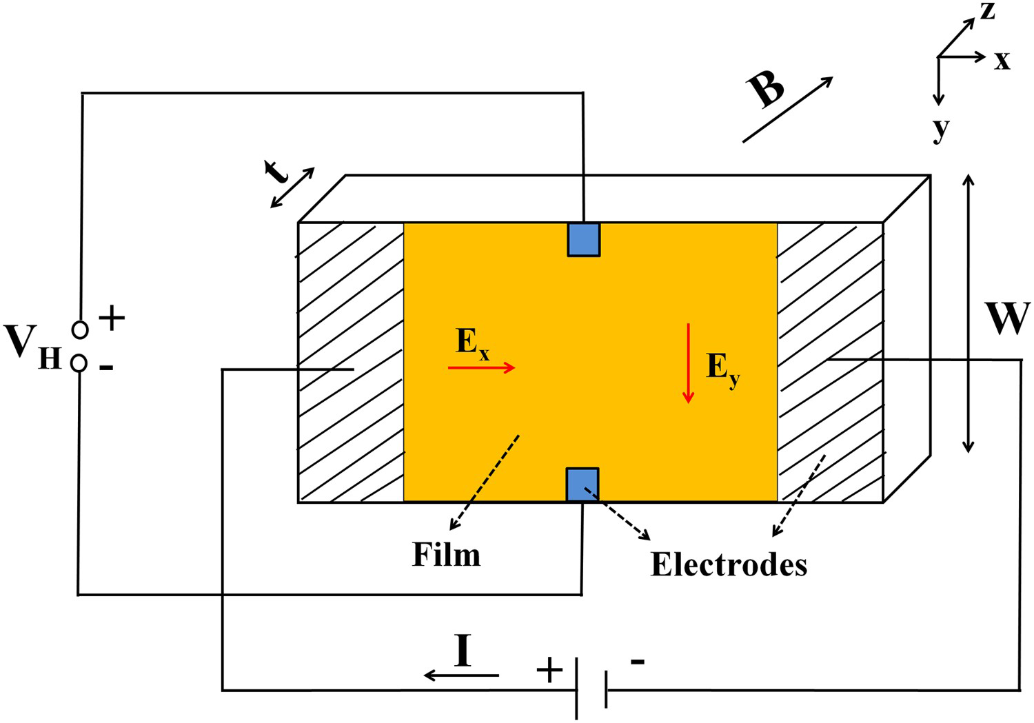
Magnetic studies
Magnetic properties of the CdS:Li thin films were determined by plotting magnetisation versus magnetic field M–H curves using a low-temperature VSM set-up. The M–H curves of the CdS:Li thin films are displayed in Figure 7. The doped films exhibited ferromagnetic behaviour with the presence of well-defined hysteresis loops. The ferromagnetic behaviour observed for the doped films might be due to the magnetic interactions between the dopant atoms or due to the substitutional spin-polarised Li+ ions occupying the CdS lattice as reported by Ravishankar et al. [26] for Fe-doped PbS thin films. Ghosh et al. [27] reported that Li+ ions induce ferromagnetism in ZnO nanowires through intrinsic structural modifications due to the creation of defects. The hybridisation between the transition metal atoms and S atoms also induces more magnetic moments in the doped films as reported by Chen et al. [28]. Owing to the decreased crystallite size values observed for the doped films, the net magnetic moment increases due to non-exact compensation of the magnetic sublattices as reported Sadoon et al. [29]. The enhanced ferromagnetic behaviour observed for the 1 wt-% Li-doped CdS thin film might be due to its decreased crystallite size value. The slight decrement in the magnetic moments observed for the 2 and 3 wt-% Li-doped films might be due to the occupancy of most Li ions at the interstitial positions and the bottom of the conduction band as reported by Vettumperumal et al. [30] for Li-doped ZnO thin films.
M–H plots of the CdS:Li thin films.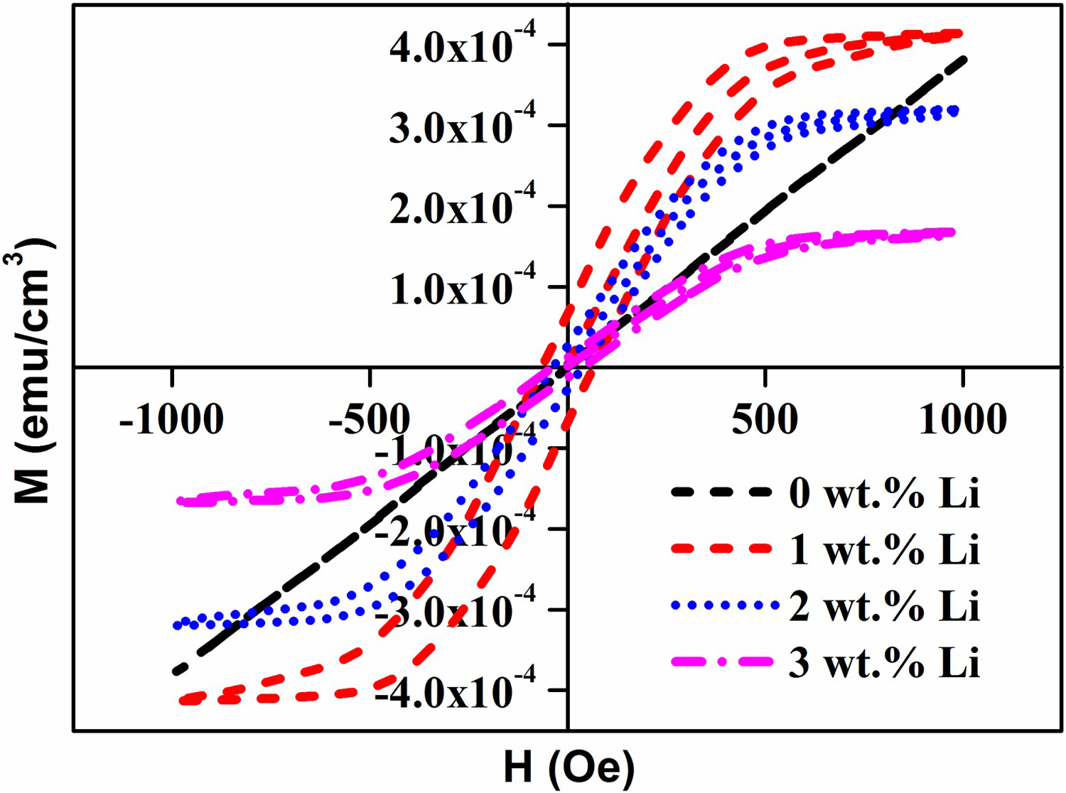
Conclusion
CdS:Li thin films with hexagonal crystal structure having (0 0 2) preferential growth were successfully deposited on glass substrates by the spray technique using a perfume atomiser. The results obtained on the structural, optical, electrical and magnetic properties of the deposited CdS:Li thin films are summarised as follows:
Decreased crystallite size was observed for the doped films. Nanoneedles were observed from the SEM images of the doped films. XPS spectrum confirmed the presence of Li in the doped films. Band gap exhibited bowing due to the dominance of Licd (acceptors) and Lii (donors). Decreased electrical resistivity is observed for the 1 wt-% Li-doped CdS thin film. The doped films showed ferromagnetic behaviour and for the 1 wt-% Li-doped CdS thin film, enhanced ferromagnetic ordering was observed.
From the obtained results, it was observed that Li doping enhanced the structural, optical, electrical and magnetic properties of CdS thin films and the CdS:Li thin films are well suited for spintronics applications.
Acknowledgements
The authors thank the Head, Department of Physics, Alagappa University for the VSM studies.
Footnotes
Disclosure statement
No potential conflict of interest was reported by the authors.