
Abstract
In this work, plasma electrolytic fluorination (PEF) was performed on AZ91 alloy in a non-aqueous NH4F-ethylene glycol (EG) electrolyte. The coating growth and the plasma discharge behaviour were investigated to understand the mechanism of PEF process. Results illustrated that the non-aqueous electrolyte determined the intrinsic characteristics of the PEF process, which resulted in the coating growth characteristics and plasma discharge behaviour distinct from those of a conventional PEO process. MgF2 compound formed from the combination of the oppositely charged ions Mg2+ from the substrate and F- form the electrolyte. The deposition of MgF2 facilitated the growth of the PEF coating with an inward-growth characteristic. The discharge was characterised by a very small size and a weak intensity of the sparks, with an electron temperature (Te) range of 3400∼3600 K. The three-type discharge model of conventional PEO processes was introduced to understand the mechanism of the PEF process.
Keywords
Introduction
The problem of global warming is pushing modern industries to reduce their greenhouse gas emissions. As a result, lightweight metals have become a boost for automotive, aerospace, transportation and many other industries [1-5]. Among them, Mg alloys are promising for sustainable manufacture in these fields, owing to the characteristics of lightweight, high performance and abundant mineral deposits [4,6]. In recent years, a great deal of works has also focused on biodegradation implants prepared from Mg alloys. These implants would make a second surgery for implant removal unnecessary, unlike in the case of conventional implant materials (e.g. titanium alloys and stainless steels) [7,8]. However, Mg and its alloys are susceptible to corrosion due to their high chemical activity, which has been considered an enormous challenge [6,9,10].
The wide applications of Mg alloys and their accompanying performance restrictions have bred a series of surface solutions. Protective coatings prepared by various surface modification technologies, such as organic coatings, electrochemical plating, anodising, conversion coatings, physical/chemical/plasma vapour deposition process and plasma electrolytic process, are available and effective for different performance demands in various fields in order to control the corrosion/degradation rate of Mg alloys [10-13].
Plasma electrolytic oxidation (PEO) is acknowledged as a unique method for fabricating oxide ceramic coatings on light metals (Mg, Al and Ti) and their alloys. The resultant PEO coatings, characterised by superior mechanical properties and chemical stability of oxide composition, can successfully protect these metal products from corrosion and wear failures and thus extend their service lives [14,15]. PEO technology has practically applied in modern industries, such as military, aerospace, automotive and 3C products. In addition, it is promising for the surface modification of orthopaedics implants and medical devices because of the natural biocompatibility of Mg, Ti and their individual alloys and oxides [7,8,16,17].
It is known that PEO processes are multifactor-controlled, such as substrate materials, electrolyte compositions and electrical parameters, and their interactions [14,18]. Among these factors, electrolyte composition has a strong influence on the resultant PEO coating in terms of its composition, microstructure and various properties [3,19-22]. Simultaneously, electrolyte characteristics also affect the coating growth and discharge events during the PEO process [19,23-26]. PEO electrolytes are generally alkaline aqueous solutions [14,27]. To date, a lot of efforts have been devoted to the development of novel electrolytes. It is the new coating-forming agents (e.g. fluorozirconate, fluorotitanate, vanadate, tungstate and stannate) that were used to replace the old ones (e.g. silicate, phosphate and aluminate) [3,15-17]. The functional additives were always incorporated into PEO electrolytes, for example, fluorides, acetates and various nano-particles [18,28-32]. However, few of them are out of the scope of aqueous solutions.
In recent years, non-aqueous electrolytes have been a new area of interest. For instance, the molten mixture of KNO3 and NaNO3 was employed to fabricate oxide coatings on 1050 Al alloy an Ti6Al4 V alloy at 280°C, respectively [33-35]. The coatings were completely composed of oxygen (O) and the substrate metal elements, without any undesirable compounds originating from electrolyte. More interestingly, molten NH4HF2 was also applied to prepare a fluoride coating on AZ31 Mg alloy at 150°C [36]. The coating was composed of almost pure MgF2, and the PEO process was designated as plasma electrolytic fluorination (PEF). These works introduced molten salts as PEO electrolytes, and thus made a breakthrough in this area. However, the high temperature of hundreds of degrees Celsius required in these non-aqueous explorations is quite harsh for equipment and dangerous for operators.
As an alternative to the molten salts, the NH4F-ethylene glycol (EG) solution at room temperature was employed as the electrolyte in our previous work [27]. Then a PEO process was carried out on AZ91 Mg alloy in the NH4F-EG electrolyte at room temperature. It unveiled a novel possibility to prepare a PEO-like but fluoride-dominated coating. Thus, the process was named as PEF. The coating was composed of pure well-crystallised MgF2, and characterised by a porous microstructure. It was attested that the coated Mg alloy performed a more desirable corrosion resistance than bare substrate.
Generally, the plasma discharge was considered as the driving force of the coating growth for a PEO process [23,37-39]. In order to investigate the discharge phenomena, an optical emission spectroscopy (OES) was employed to obtain the discharge information. Then the electron temperature (Te) of plasma could be calculated according to the Boltzmann law, which was elevated up to thousands of degrees Kelvins [14,26,38,40]. As a result, the compounds of PEO coatings originating from chemical and electrochemical depositions were finally sintered into ceramic phases. All these experimental results were utilised to build and correct the proposed theoretical models [14,26,38,40]. Owing to these achievements, it is well-founded to focus on the electrolyte characteristics, coating growth and discharge behaviour, in order to gain insight into the novel PEF process.
The study on non-aqueous PEO electrolytes at room temperature has been carried out in our previous work [27], but the study on the mechanism was absent. The current work attempted to investigate the relationship between the coating growth and the plasma discharge behaviour, in order to illustrate the mechanism of the plasma process preliminarily.
Experimental
Preparation of PEF coating
A fresh ethylene glycol (EG) solution of 8 wt% desiccated NH4F was utilised as electrolyte, with a conductivity and pH value of 5.35 mS cm−1 and 7.42 at 25°C, respectively. Samples, with dimensions of 25 × 25 × 8 mm3, were cut from the commercial AZ91 Mg alloy ingot (nominal composition in wt-%: 8.3–9.7 Al, 0.35–1.0 Zn, 0.15–0.5 Mn, ≤0.1 Si, ≤0.03 Cu, ≤0.002 Ni, ≤0.005 Fe, and balance Mg). They were polished up to 2000 grade SiC abrasive papers, washed with distilled water, degreased in ethanol ultrasonically and dried in warm air, respectively. The PEF process was performed using a conventional pulsed bipolar PEO power supply (Beijing Jinhu Technology Co. Ltd, JHMAO200H). The positive current density was kept at 8 A dm−2, while the negative current was 0 constantly. The frequency and duty cycle were 100 Hz and 20%, respectively. The electrolyte temperature was kept at 25 ± 2°C by means of a magnetic stirrer and a stainless tube cooling system.
Characterisation of PEF coating
The coating thickness was determined by the average value of 10 random test points on the coated samples by a thickness gauge (ElektroPhysik MiniTest 1100). The surface and cross-sectional morphologies of the coatings were observed by a scanning electron microscope (SEM, JEOL JSM-5600LV), and the elemental contents and mappings were detected by an X-ray energy dispersive spectrometer (EDS, Oxford Instruments X-MaxN 80) attached to the SEM. The phase compositions of the coated samples were determined by an X-ray diffraction spectrometer (XRD, PANalytical Empyrean) in the grazing incidence mode with a constant incidence angle of 2°, while the un-coated substrate was measured in the common bulk/powder mode.
A stylus profilometer (KLA Alpha-Step D500) was used to measure the 2D profile of the coating surface, with a sampling length of 5 mm and a step size of 0.1 μm. The measurement was repeated three times, and the arithmetic mean value was calculated as the surface roughness (Ra) of the coating.
Characterisation of PEF discharge
During the PEF process, the discharge spectra were captured by an optical emission spectrometer (OES, Ideaoptics PG2000-Pro-EX) with a spectral resolution of 1 nm in a wavelength range of 200–1100 nm. Considering the weak luminance of the discharge sparks, it was necessary to optimise the integration time of spectrum acquisition for a desirable signal-to-noise ratio. The integration time of 10 s was found to be appropriate for this purpose.
The analysis of the discharge spectra was based on the National Institute of Standards and Technology Atomic Spectra Database (NIST-ASD, Version 5.7.1), which provided open access and search capability for NIST critically evaluated data on atomic energy levels, wavelengths, transition probabilities and other relevant parameters.
A digital camera (Nikon D7000 equipped with Nikkor AF-S DX 18–105 mm f/3.5–5.6G) was utilised to record the photographs and video of discharge sparks. The photographs were recorded in the optimised manual mode, while the video was in an auto mode.
Results
Growth dynamics of PEF coating
Figure 1 shows the variations of the voltage and the coating thickness with the processing time during the PEF process. The voltage increased with time while the growth rate gradually slowed down. The voltage-time response underwent a sharp increase within the initial 0.75 min (Stage I), a transitional stage within the following 3.25 min (Stage II) and a slow increase within the final 11 min (Stage III). The threshold voltages of Stages II and III were approximate 270 and 470 V, respectively. The coating thickness also increased with time. The final voltage and coating thickness were approximately 565 V and 16.4 μm during a 15 min processing time, respectively.
Variations of voltage and relevant coating thickness with time.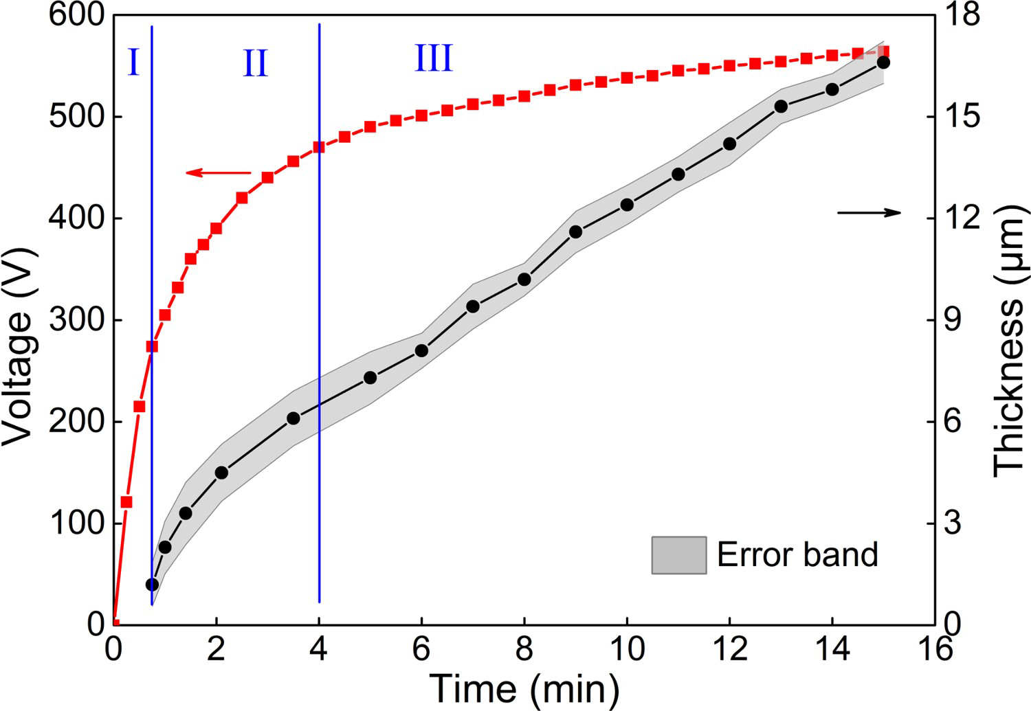
Morphological variation of PEF coating
Figure 2 shows the visual appearance of the coatings at different voltages during the PEF process. Compared with the shining metallic lustre on the polished bare AZ91 Mg alloy substrate, a great number of scattered white spots could be seen on the sample surface at 150 V, indicating that the substrate was locally coated. These white spots continuously increased in number and size with the increase of voltage, and thus spread over the entire surface when the voltage increased to 200 V. The individual coated area grew up and expanded further at 250 V. The sample surface was completely covered by a white coating when the voltage was up to 300 V. With a further increase in voltage, there was no macroscopic difference in appearance for the subsequent coatings.
Visual appearance of PEF coatings at different voltages.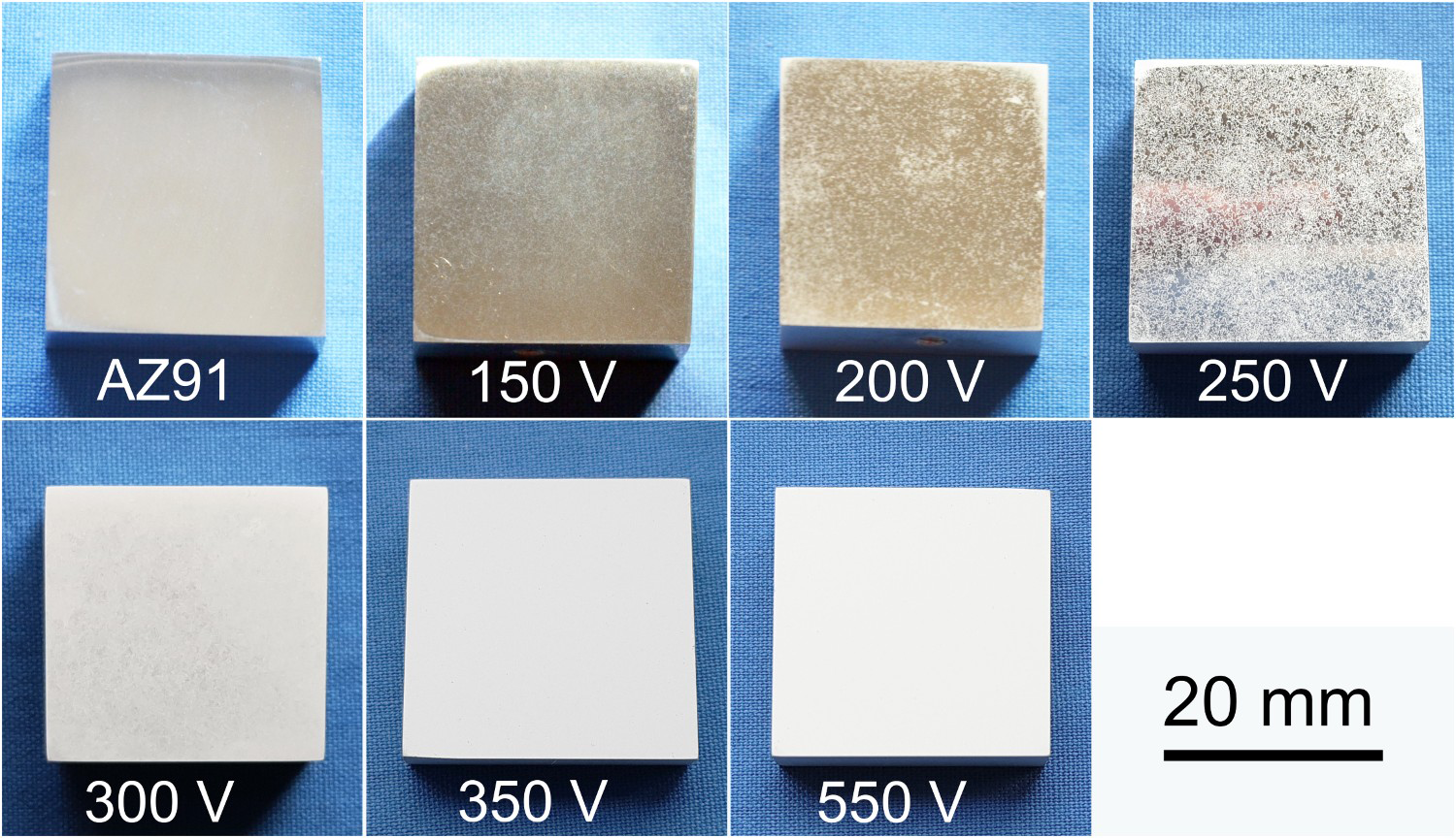
Figure 3 shows the microstructural and elemental variation of the coating during the PEF process, corresponding to the visual-appearance variation shown in Figure 2. As shown in Figure 3(a), α-Mg and β-Mg17Al12 phases could be observed and distinguished on bare AZ91 substrate, according to the elemental distribution mapping of Al [41]. When the voltage of 150 V was applied, it could be seen that the sample surface was covered with a thin film which was mainly composed of Mg and F elements (Figure 3(b)). There were also some locally accumulated micro-particles as marked by the arrows. This microstructure was appeared within the β-Mg17Al12 phase areas before α-Mg phase areas, according to the relevant EDS mapping as shown in Figure 3(b). As the voltage rose further to 200 V, a large number of micro-pores appeared on the sample surface as shown in Figure 3(c), but some areas were not yet microporous as shown by the dark areas. The relevant elemental mapping indicated that there were more micro-pores within the β-Mg17Al12 areas (as marked by the circle) than the α-Mg areas. This structural characteristic illustrated the heterogeneous growth of the initial PEF coating during Stage II as defined in Figure 1. When the voltage increased to 250 V, the sample surface was almost completely covered by a porous coating as shown in Figure 3(d). However, the microstructure and the composition of the coating were not uniform at this stage. There were obviously microstructural differences between the α-Mg and β-Mg17Al12 phase areas. As a result, the β-Mg17Al12 areas (as marked by the rectangles) were still distinguishable from the α-Mg phase areas, according to the relevant elemental mapping. This microstructural difference gradually disappeared as the voltage increased, as shown in Figure 3(e∼f). It could be seen from Figure 3 g that the coating had a uniform porous microstructure. Up to the end at approximately 550 V (Figure 3 h), the coating showed no obvious changes in microstructure.
Surface microscopy and elemental mappings of PEF coatings at different voltages: (a) 0 V, (b) 150 V, (c) 200 V, (d) 250 V, (e) 350 V, (f) 400 V, (g) 450 V, (h) 550 V.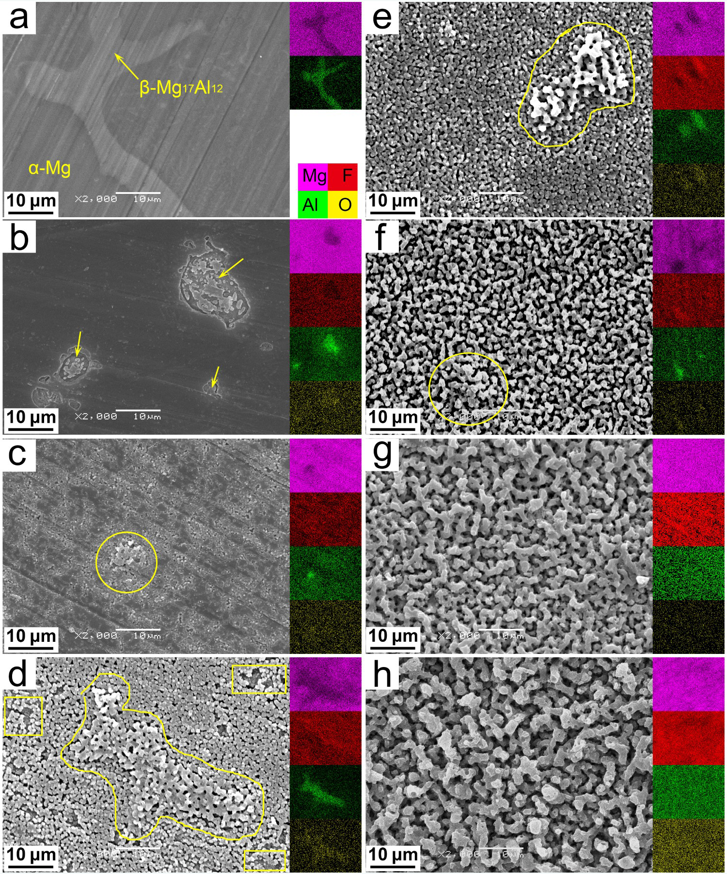
Figure 4 shows the 2D surface profile and the calculated surface roughness (Ra) of the coatings at different voltages. Corresponding to the surface morphologies of the coatings as shown in Figure 3, the porous microstructure was reflected by the fluctuations on the profiles. As shown in Figure 4(a), the profiles of the coated samples showed more fluctuations than that of the un-coated substrate (0 min). On the other hand, the baselines fluctuated more wildly as the processing time prolonged, indicating that the exceptional peaks and valleys away from the baseline were submerged gradually. Quantitatively, the surface roughness of each profile was calculated and shown in Figure 4(b). The Ra value continuously increased from 103.51 nm (the substrate surface) to 1140.72 nm (the final coated surface). In detail, the Ra values were lower than 400 nm with a small error when the processing time was less than 3 min. After that, the Ra values were higher than 400 nm with a large error. Interestingly, the relevant voltage was approximate 440 V at 3 min as shown in Figure 1. At the same time, the coating presented a uniform microstructure as shown in Figure 3 g. In summary, the surface profile and roughness measurement also indicated that the coated sample surface tended to be uniform as the processing time prolonged.
(a) 2D profile and (b) surface roughness of the coated sample in different processing times.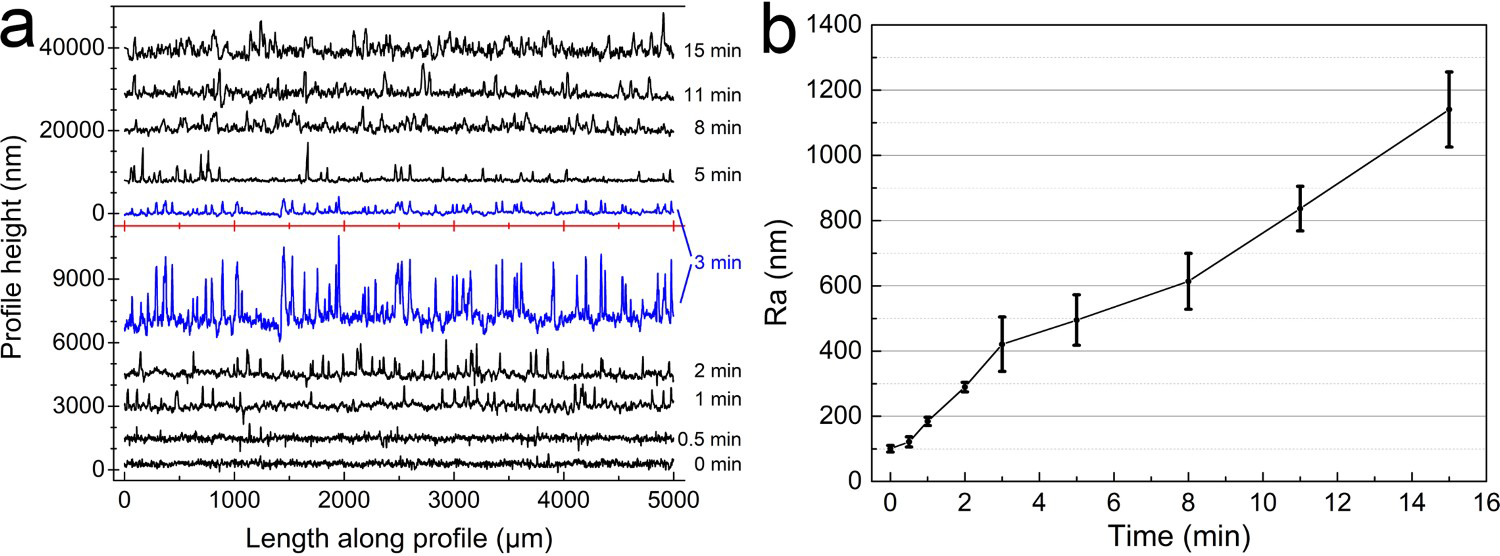
Figure 5 shows the cross-sectional microscopies of the coatings at different voltages, in order to further investigate the early coating growth. It could be seen from Figure 5(a1) that there was a thin porous layer formed at 200 V. It corresponded to the concentrated band of fluorine with a depth of less than 1 μm as shown in Figure 5(a2). The profile approximately marked the substrate/layer interface, although there was no obvious boundary between the substrate and the porous layer. As shown in Figure 5(b), a complete coating formed at 250 V, which was distinguishable from the AZ91 substrate by a distinct interface. The coating was about 1 μm in thickness, and seemed more compact and uniform than before. When the voltage increased to 350 V, the coating (Figure 5(c)) showed no difference from the final PEF coating formed at 550 V (Figure 5(d)) except for its thickness. As shown in Figure 5(b1, c and d), the fluctuations near the coating surface were correlated with the micro-pores observed in the surface view (Figure 3). In summary, there was a consistency of the morphological variation of the PEF coating in the cross-sectional (Figure 5) and surface (Figure 3) microscopies.
Cross-sectional microscopy of PEF coatings at different voltages: (a1) 200 V, (b1) 250 V, (c) 350 V, (d) 550 V. Related fluorine mappings: (a2) that of (a1), (b2) that of (b1).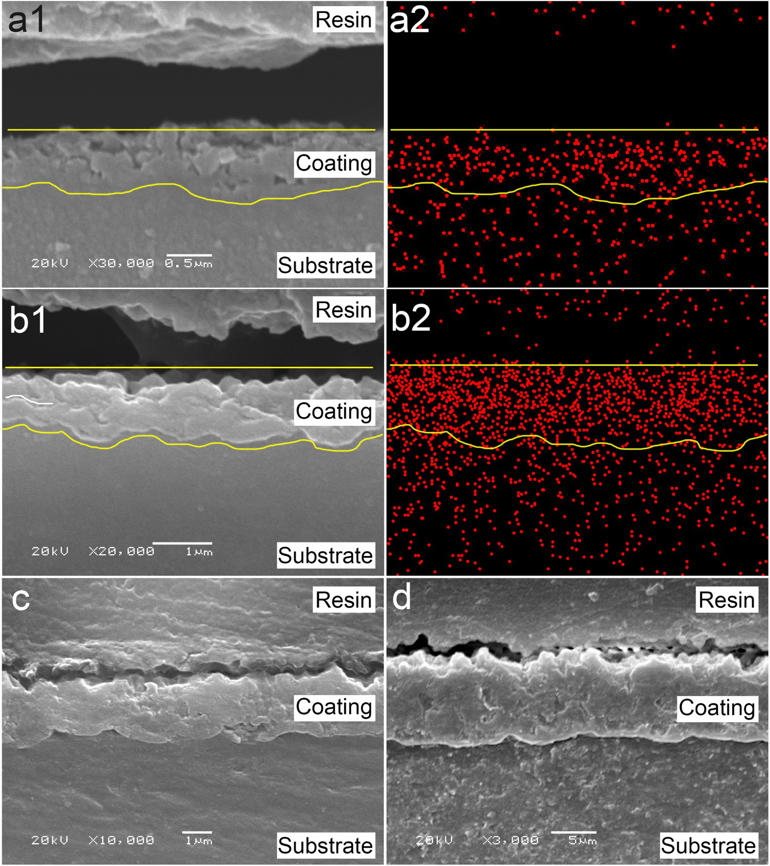
Composition variation of PEF coating
Figure 6 shows the elemental compositions of the PEF coatings formed at different voltages as shown in Figures 2 and 3. The AZ91 column refers to the un-coated substrate without voltage applied. There was 2.2 wt-% of O resulting from unavoidable natural oxidation except for Mg and Al. It could be seen that all the elements, e.g. Mg, Al, F and O, were detected in the samples when the voltage was applied. As the increase of voltage, the contents of Mg and Al decreased sharply, while that of F element increased substantially. When the voltage was above 350 V, the elemental content did not change with the further increase of voltage. Eventually, the contents of Mg, F and Al were stabilised at approximate 37.8, 57.4 and 2.5 wt-%, respectively. In the case of O, the content increased up to 4.0 wt-% at 200 V and then dropped to the initial level of 2.2 wt-% during the PEF process. In addition, the F/Mg ratio was stabilised at 1.52 for the sample surface at different voltages, which was very close to the constituent of MgF2 (1.56, in wt-%). It suggested that the PEF coating might be mainly composed of the MgF2 phase.
Elemental contents of PEF coatings at different voltages.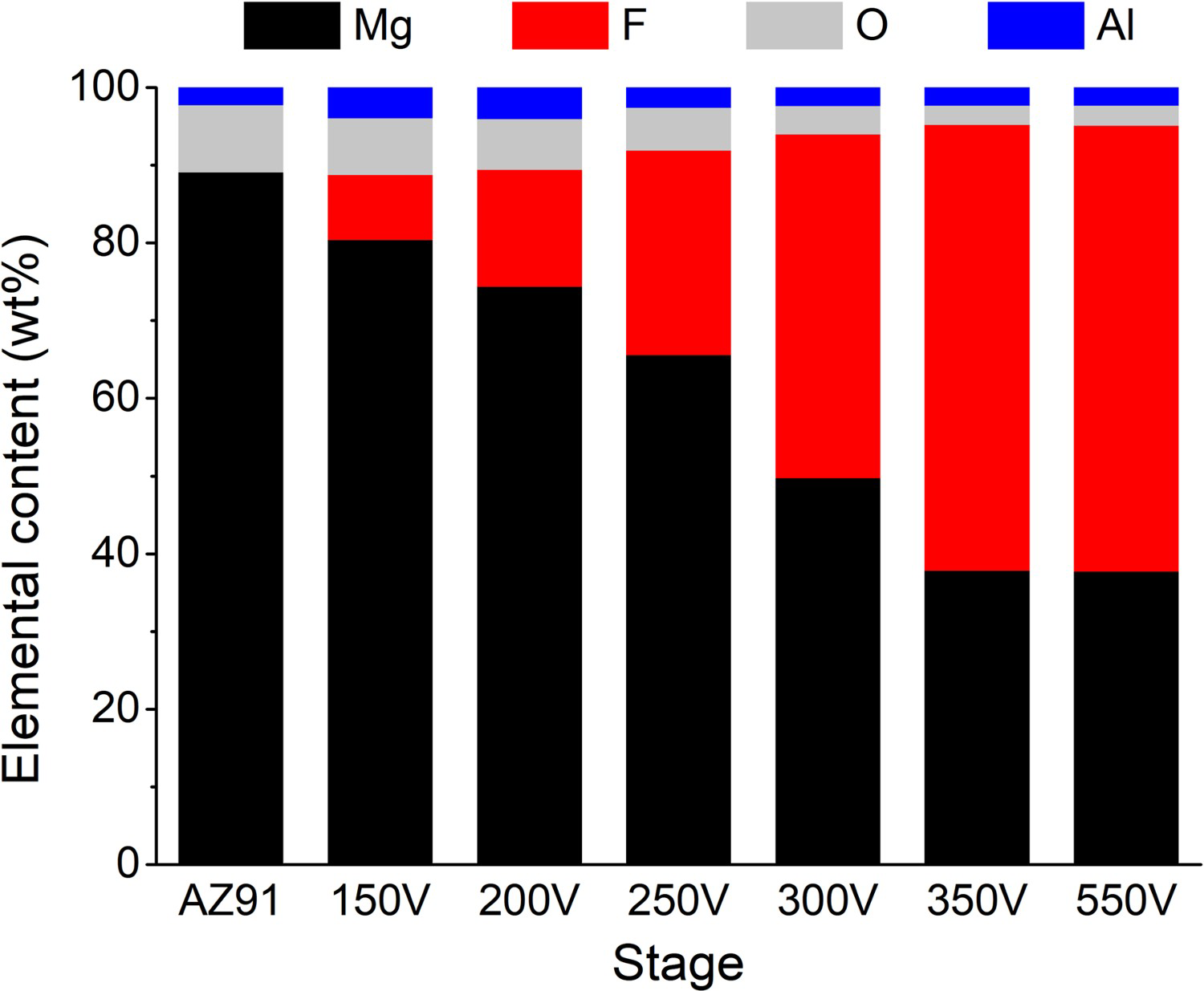
Figure 7 shows the XRD patterns of the coated samples at different voltages and the un-coated substrate. For the un-coated substrate, the diffraction peaks corresponding to Mg phase were identified in the AZ91-marked pattern. For the samples coated at 250 and 350 V, the humps (as marked by the dashed line boxes) appeared around 27.23, 40.43 and 53.49° of the 2Theta ranges. They were corresponding to MgF2, according to the powder diffraction file of MgF2 (PEF#70-2269). This suggested that an MgF2 coating was generated on the substrate. However, these marginal signals from MgF2 in the initial PEF coating were hard to be distinguished from the strong signals from the substrate Mg, because the coatings were too thin as shown in Figures 1, 2 and 5. For the samples coated at 450 V, the diffraction peaks corresponding to MgF2 were evidently detected, instead of the Mg peaks. And the MgF2 signals increased with the voltage increase to 550 V. Therefore, the coating was predominantly composed of MgF2, which was agreed with the EDS results.
XRD patterns of PEF coatings at different voltages.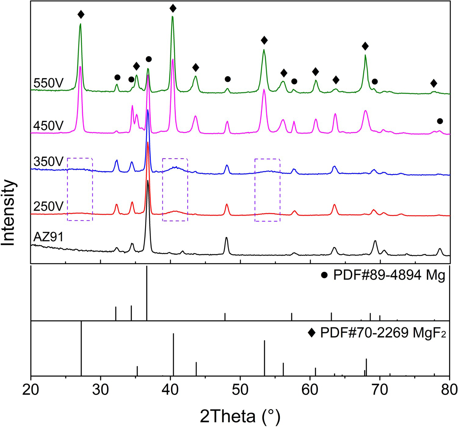
Growth direction of PEF coating
Figure 8 shows the growth characteristic of the PEF coating prepared at 550 V, which was investigated by means of a well-designed jig [19]. It was clarified that most part of the coating was below the original surface of the substrate surface as marked by the dashed line, according to the cross-sectional view. This was further confirmed by the relevant EDS mapping of Mg and F. Therefore, it could be concluded that the PEF coating was dominated by an inward growth.
Growth characteristics of PEF coating at a final voltage of 550 V.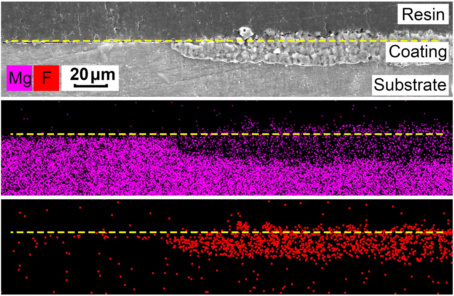
Characterisation of discharge sparks
Figure 9 shows the optical images of the discharge sparks at different voltages during the PEF process, and the relevant video is also provided in supporting information (Movie s1). Several scattered sparks appeared on the sample surface at 120 V, indicating that the discharge occurred. As the voltage increased, more discharge sparks appeared and got brighter simultaneously. When the voltage increased to 450 V, the countless sparks completely spread over the sample surface. Eventually, the sample surface was covered by more discharge sparks than ever at 550 V. The sparks were characterised by tiny size, weak intensity and low luminance during the whole process.
Optical images depicting the appearance of discharge sparks during the PEF process at different voltages: (a)120 V, (b) 150 V, (c) 250 V, (d) 350 V, (e) 450 V, (f) 550 V.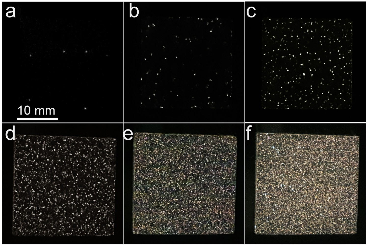
The response of the discharge spark count to the voltage was described by a quasi-quantitative statistical analysis as shown in Figure 10. Within the error range, the spark count kept an approximately linear growth trend in the voltage range from 120 to 450 V in the coordinates of logarithmic vertical axis. In other words, the spark count experienced an exponential growth in fact. It was nearly doubled in each 50 V increase of the voltage from 150 to 450 V, which was also valid for the 30 V increase from 120 to 150 V.
Statistical analysis of discharge sparks during the PEF process.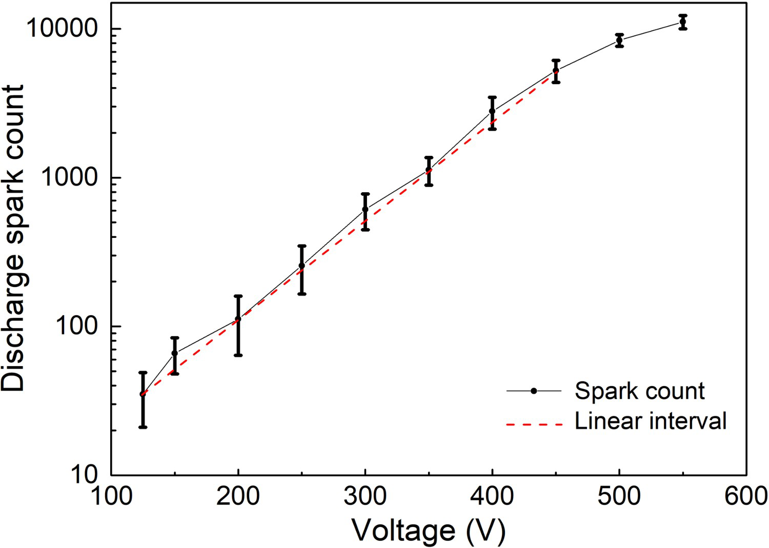
Characterisation of OES spectra
Figure 11 shows the OES spectra of the discharge sparks to investigate the discharge behaviours of the PEF process. When the voltage rose to approximately 300 V, the discharge spectrum was shown as curve S1. The subsequent spectra were shown as curve S2∼S5, and the final state of the PEF process with a voltage of 550 V was recorded as curve S6. According to the NIST-ASD [42], the lines of atomic species were identified, where the suffixes I and II were, respectively, referred to the neutral and singly ionised state of each atom. The lines of the molecule and radical species in the spectra were confirmed from the published references [43-50].
OES spectra of discharge sparks during the PEF process.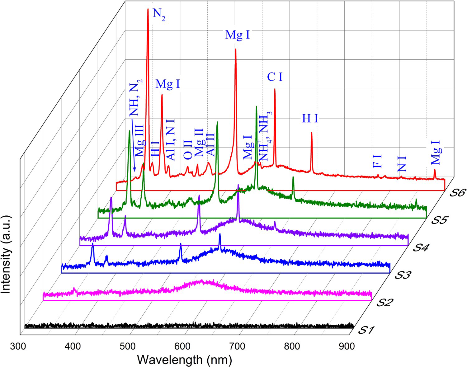
It can be seen that the spectral intensity increased gradually from curve S1 to curve S6. All the emission signals of the elements from the AZ91 substrate and the NH4F-EG electrolyte were detected, except for fluorine.
In curve S1, the spectrum almost overlapped the base line at a zero level, due to the weak luminance of the discharge sparks as shown in Figure 9. As a result, no emission signals could be identified from the spectrum. As shown in curve S2, N2 line (358.7 nm) and Mg I line (518.4 nm) appeared in the spectrum, and there was a protuberance in the range of 400∼750 nm. The tip of the protuberant region was very close to C I line (589.2 nm). In curve S3, the C I line (589.6 nm) was distinguishable from the relevant protuberant region, and another strong line of Mg I appeared at 383.8 nm. Afterwards, the H I line appeared at 656.3 nm as shown in curve S4. The marginal lines of Mg III (349.8 nm), Al I (396.1 nm), N I (429.3 nm), Mg II (448.1 nm) and Mg I (880.6 nm) could be identified in curve S5. There were also some marginal signals appeared in curve S6, which were the radical and molecular lines of NH (336 nm), N2 (337 nm), NH3 (563.9 nm) and NH4 + (563.9 nm). Also, the trace of O I lines at 777.5 and 844.6 nm were detected.
It should be noted that the protuberant region in the range of 400∼750 nm appeared universally at different voltages as shown in curves S2∼S6. This phenomenon reflected the continuum emission signals from the discharge event, and resulted from the collision-radiative recombination of electrons (bound-free transitions) and the Bremsstrahlung radiation (free-free transitions) [51-53].
Calculation of electron temperature (Te)
Based on the characteristics of the OES spectra, the Mg I lines at 383.8 and 518.4 nm were used to calculate the temperature (Te
) of plasma electrons, as the following equation [26,54,55]:
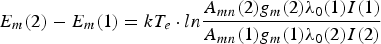
Parameters of Mg I lines for calculating Te .
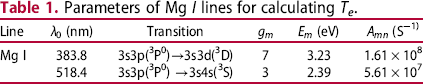
As a result, the calculated Te was in the range of 3400∼3600 K. Empirically, the ratio of kT/ΔEm was considered as an indication of the relative error in the calculation of Te . The result would be accurate and credible only if the ratio was less than unity [26]. In this work, the ratio (kT/ΔEm) was 0.414, indicating that the Te range was valid.
Discussion
Multistep growth of PEF coating
Similar to a conventional PEO process [3,14,19], it could be concluded that the PEF coating underwent a multistep growth according to the comprehensive analysis of the growth dynamics, morphological and composition variations as illustrated above. The growth process of the PEF coating (as shown in Figure 3) could be divided into passive period (below 150 V), transitional period (150∼250 V) and growth period (above 250 V). Here, the transitional period referred to the transition from a passive film to the initial PEF coating. This growth behaviour of the PEF coating was described schematically in Figure 12.
schematic diagram of the PEF process: (a) passive film formed during the passive period, (b) initial PEF coating formed in the transitional period, (c1) SEM image of the PEF coating and the relevant schematic diagram (c2), (d) plasma discharge behaviour (NH species refers to the species related to the decomposition of NH4
+ radical, and EG species refers to the species related to the decomposition of EG).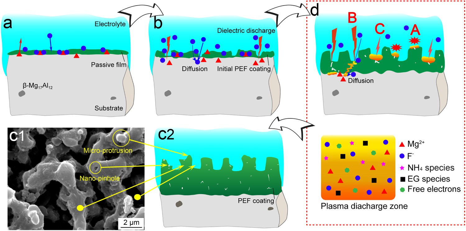
Figure 12(a) illustrates that the substrate reacted with the electrolyte under a relatively low voltage during the passive period. As the voltage increased above a threshold value, the passive film was break down. As a result, the microporous structure appeared, suggesting that the initial PEF coating generated on the substrate as shown in Figure 12(b), because the micro pores were considered as a record of the discharge channels [20,26,38,56]. After that, the PEF coating continued to grow accompanying the discharge event as shown in Figures 12(c,d). The more details of these periods would be discussed as below.
Passive effect of non-aqueous electrolyte
In the non-aqueous NH4F-EG electrolyte, the basic salt NH4F was rich in F and easy to ionise into F- anions, but oxygen-free as well. On the other hand, EG was a covalent compound whose atoms are combined by covalent bonds. As a result, it was difficult for EG to ionise into active O anions or O-containing groups, although its molecules contained abundant oxygen. In other words, the NH4F-EG electrolyte provided a desirable environment for fluorination rather than oxidation, compared to conventional PEO electrolytes [3,14,19,41,54].
The conductivity of the NH4F-EG electrolyte was 5.35 mS cm−1 at 25°C, in the same level of common PEO electrolytes [3,19,41], whereas that of fresh EG was 0.20 μS cm−1 at 25°C as we tested. On the other hand, the molar concentration of the NH4F-EG electrolyte was approximate 2.4 mol L−1, which was about tens of times higher than common aqueous PEO electrolytes [3,19,41]. Thus, it can be inferred that the dissolved NH4F ionised in EG as follows:
According to the optical (Figure 2) and microscopic (Figure 3(b–c) and Figure 5(a)) appearances of the samples, there was a thin fluoride film generated on the sample surface and covered its metallic lustre, suggesting the passivation of AZ91 substrate in the PEF electrolyte during the passive period. This was schematically shown in Figure 12(a), and the reaction process could be described as follows:

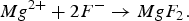
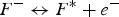
Accompanying the natural passivation before the discharge event occurring, the applied voltage would facilitate the dissolution of the anodic substrate to release Mg2+ ions as follows [14,18,57,58]:
Simultaneously, F- ions in the electrolyte migrated to the anodic surface under the effect of the external electrical field generated by the applied voltage [22,37]. Then the dissolved Mg2+ ions combined these F- ions and deposited on the substrate surface, thus contributing to the formation of the passive film [59]. The combination process could be described as follows:
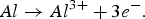
As expected, the alloying element Al in the β-Mg17Al12 phase would undergo similar reactions as Mg atoms as follows:

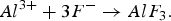
However, the AlF3 compound was too little to be detected by XRD, because there was only a few (3 wt-%) Al in the coating as proved by EDS.
The Pilling-Bedworth ratio (PBR) of the passive film, which was equal to the ratio of the molar volume of MgF2 to that of Mg, was about 1.39. In other words, the passive film was compact enough to completely cover the substrate surface [9,60]. At the same time, the non-conducive passive film would play a role of the dielectric layer [38,61-63], and result in a sharp voltage increase between the anode substrate and the cathode, as reflected by stage I in the voltage-time response in Figure 1. The passive film was observed until the plasma discharge occurred on a large scale, as shown in Figure 3(b–c) and Figure 9(a–b).
PEF coating growth facilitated by plasma discharge event
The non-conducive passive film was a requisite for the discharge breakdown [38,61-63]. On one hand, a lot of F- anions accumulated on the anode substrate surface under the influence of the electric field between anode and cathode. On the other hand, these accumulated F- anions also acted as quasi-cathode for the electric field between the interfaces of the substrate/film and film/electrolyte [33,64]. As the voltage increased further, more and more electric charges accumulated on both sides of the passive film. Once the accumulated charges exceeded a critical value, the dielectric breakdown of the passive film would occur, accompanied by visible discharge sparks as shown in Figure 9. At the same time, the discharge channels were recorded as micro-pores on the sample surface [20,26,38,56] as shown in Figure 3(b–h). As a result, the initial PEO coating was born from the passive film, which was described in Figure 12(b).
Owing to the plasma discharge event, the chemical/electrochemical passivation was replaced by the plasma electrolytic process involving electrochemical reactions, plasma chemical reactions and thermochemical diffusion simultaneously [37,38,65]. The plasma chemistry of the discharges facilitated strong ionisation and charge transfer through the PEF coating (between the substrate/coating and the coating/electrolyte interfaces). As a result, abundant Mg2+ ions were released from the AZ91 substrate as described by Equation (4). Together with the plasma chemical reactions, the thermochemical diffusion of the Mg2+ and F- ions ensured mass transfer for the continuous electrochemical reactions, which resulted in the combination and deposition of the coating compounds as described by Equations (5) and (8).
The electrochemical reactions mostly occurred at the coating/electrolyte interface. For a conventional PEO process, a considerable amount of compounds was decomposed from the electrolyte anions, which resulted that the outward growth of the PEO coating was rarely absent [19,38]. On the contrary, the oxidation of the substrate usually led to an inward growth of the PEO coating. In this work, the PEF coating was characterised by an absolutely inward grew as shown in Figure 8. This was because F- ions in the PEF electrolyte directly reacted with Mg/Mg2+ from the substrate, which contributed to the inward growth of the PEF coating. On the other hand, the simple F- ion could no longer decompose into other smaller molecular compounds. As a result, no compounds would be deposited from the electrolyte to contribute to an outward growth of the PEF coating.
According to the Clausius–Clapeyron equation, the lower electron temperature (Te = 3400∼3600 K, as calculated) indicated a lower pressure in the PEF process, compared to conventional PEO processes (Te = 4000∼10,000 K, above 102 MPa) [25,40,55]. In other words, more molten compounds (a mixture of substrate, coating and electrolyte) would solidify in the discharge channels as shown in Figure 12(d), rather than being ejected out of the channels and deposited as the pancake-like microstructure on the coating surface. This also contributed to the inward growth of the PEF coating.
Thermodynamic parameters of fluorides and oxides of Mg and Al.
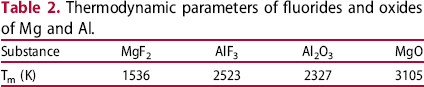
It can be seen that the Te was much higher than the Tm of the fluorides of the substrate metal elements or the pollutant oxides [27]. In other words, such an elevated plasma temperature, associated with the ultra-high pressure [25,40,55], was sufficient to melt and sinter the coating compounds during the PEF process. Therefore, the coating compounds transformed into ceramic phases.
Finally, the PEF coating grew to a certain thickness as shown in Figure 12(c). Its microstructural details [27] were shown in Figure 12(c1) (magnified view of Figure 3(h)), and the relevant schematic diagram was shown in Figure 12(c2).
Discharge types and coating's microstructure
According to the well-acknowledged three-type discharge model proposed by Hussein [14,19,26,38], the irregular-shaped micro-pores, micro-protrusions and the nano-pinholes of the PEF coating could be related to the discharge characteristics. During the PEF process, the discharge events were categorised into three types with different intensities and originations as the marks (A∼C) referred in Figure 12(d).
The irregular-shaped pores were the tracks of open channels which were resulted from the B-type penetrative discharges. They occurred around the substrate/coating interface or the micro-pores in the inner layer of the coating with relatively high intensity. This type of discharge penetrated the PEF coating, and its thermal effect melted the discharge channels and the coating/substrate interface due to the electron avalanches. At the same time, the F- anions were drawn into the channels by the strong electric field (of the order of 106 V m−1) [37,51]. However, the Mg2+ cations would not be extensively ejected out of the channels into the electrolyte, because PEF was a much ‘softer’ discharge process compared to conventional PEO. The calculated Te (3400∼3600 K) was even lower than the minimum plasma temperature of PEO [25,40,55], which suggested a lower pressure in the discharge channels according to the Clausius–Clapeyron equation. Thus, the reaction product MgF2 generated and deposited around the wall and bottom of the discharge channels after cooling and solidifying, as shown in Figure 12(d), rather than being ejected out of the channels and deposited as the pancake-like microstructure on the coating surface [37,51].
The A-type and C-type discharges were denoted as surface discharges and derived from a gas breakdown. The A-type discharge correlated to the nano-pinholes on the coating surface, while the C-type discharge correlated to the micro/nano-pinholes on the walls of the irregular-shaped micro-pores. Both of them were softer than B type. The most possible advantage of these two types of discharge was to heal the surface (by A-type) and internal (by C-type) defects, respectively. As a result, there were no micro cracks and other micro defects observed anywhere in the coating, although stresses accompanied the process.
OES analysis of the PEF discharge
According to the PEO breakdown theory [14,37,38,51], the electrolyte would pour in the discharge channels. Once the breakdown occurred, electrolyte constituents and all the coating compounds would be locally decomposed to active and free ions (atoms or radicals), caused by the elevated temperature (3400∼3600 K, as calculated) and the high pressure within the channels (above 100 MPa [25,40,55]). Corresponding to the OES measurement, the spectral signals of discharge originated from the radiation of the active ions. In result, all the spectral signals of the species, from both of the substrate and the electrolyte, were detected and identified in Figure 11.
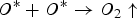
There was a marginal signal of the neutral F atoms, rather than F- ions, in the OES spectra. One of the most possible reasons might be that the F- ions could easily bind with Mg atoms and Mg2+ ions as described in Equations (3) and (5). Owing to the electron-impact ionisation of the plasma environment [51-53], a small quantity of F- ions reversibly released free electrons,
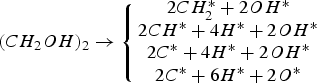
Owing to the electron-impact, ion-impact and thermal-impact dissociations in the plasma environment, the NH4
+ radicals might decompose as follows [45,50]:
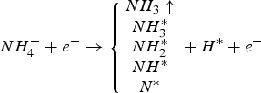
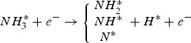
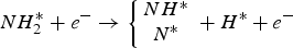


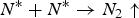

As a result, the signals originated from NHn species (n = 1, 2, 3 and 4), N2 and H were present in the OES spectra. The decomposed active H and species combined to release hydrogen (H2).
Similarly, the EG molecules decomposed into CH2, OH, C, CH and H species as follows [65,67]:
In our previous work [27], it was reported that the trace of O in the elemental content of the PEF coating was attributed to the unavoidable natural oxidation of the substrate. According to Equations (17) and (18), the oxygen released from the decomposition of EG might be another reason.
Conclusion
In the current work, the characteristics of the PEF process, in terms of the coating growth and the plasma discharge, were investigated. Then the PEF mechanism was revealed preliminarily.
The non-aqueous NH4F-EG electrolyte determined the intrinsic characteristic of the PEF process, resulting in its distinctive coating growth and plasma discharge behaviour compared to those of conventional PEO processes. The PEF coating growth underwent passive period, transitional period and growth period successively, in which the passive film transformed into the initial PEF coating as the plasma discharge occurred. The coating was characterised by an inward growth, because the process was predominated by the fluorination of the Mg alloy substrate. PEF was a much ‘softer’ discharge process compared to a conventional PEO process. Its discharge sparks were characterised by tiny size and weak intensity during the whole process. And its plasma electron temperature was in the range of 3400∼3600 K, which contributed to sintering the coating compounds into ceramic phases. The relationship between the coating growth and the discharge behaviour during the PEF process could be explained by the three-type discharge model of conventional PEO processes as well. The penetrative discharges led to the irregular micro-pores in the coating, and the surface discharges resulted in the micro/nano-pinholes in the surface layer of the PEF coating.
CRediT authorship contribution statement
Footnotes
Acknowledgements
The authors thank to the financial support from the National Natural Science Foundation of China (grant number 52071325). The authors are grateful to Dr Dongmei. Li, Dr Xiaojuan Huang, Mr Guantao Kou for the characterisations, Dr Xiangli Wang and Dr Baixing Liu for the discharge spectral analysis, and Ms Xiaohui Li for the helpful discussion about the artworks.
Disclosure statement
No potential conflict of interest was reported by the author(s).