
Abstract
Spintronics has emerged in the last two decades as both an extremely fruitful direction of research into the properties and usefulness of the spin degree of freedom of the electron as it can apply to the exponentially expanding world of electronics. Spintronics has infiltrated almost every household in the form of the read head sensors for the hard drives that inhabit every desktop and most laptop computers. Embedded magnetic random access memory (MRAM) and in-plane STT-RAM are rapidly replacing SRAM in a host of applications that do not require ultra-dense memories. Soon these embedded spintronic memories will permeate the cell phone market because they are much denser than SRAM, offer lower power at only slightly lower speed and are non-volatile. The present work in spintronics at most of the mainstream semiconductor companies and foundaries is focused on the development of perpendicular STT-MRAM, as a universal memory that can compete with the mainstream memories and surpass them in several key metrics. Several innovative ideas are presented where spintronics may have an impact because of the uniqueness of the approach. Nanomagnetic logic and storage may offer extremely high densities at very low power. Spin-torque oscillators are a very novel approach to pattern recognition that may be relevant for handling massive data sets. The spin of the electron may also be on the critical path for quantum computation or communication, another revolutionary change in how we process information.
Abbreviations
anisotropic magneto-resistance: electrical resistance of a material that is dependent on the angle between the direction of electric current and direction of magnetisation.
stability factor: defined as K eff V/k B T, which represents the thermal stability of the magnetisation of the free layer in either spin value or magnetic tunnel junction.
minimum lithographic feature size 2-minimum device size
giant magneto-resistance: Electrical resistance of a spin valve that is dependent on the magnetisations in the two adjacent magnetic layers.
hard disk drive
anisotropy field
In plane-perpendicular magnetic anisotropy
maximum Josephson critical current
Josephson magnetic random access memory
magnetic Josephson junction
magnetic quantum cellular automata
saturation magnetisation
magnetic tunnel junction
magnetic random access memory
perpendicular magnetic anisotropy
perpendicular magnetic tunnel junction
quantum cellular automata
reconfigurable array of magnetic automata
rapid single flux quanta
spin-torque nano-oscillator
spin torque transfer magnetic random access memory
tunnel magneto-resistance: electrical resistance of a magnetic tunnel junction.
Introduction – what is spintronics
Spintronics stands for SPIN TRansfer electrONICS, and was introduced as a term in 1996 as the name of a Defense Advanced Research Projects Agency (DARPA) project to develop both a non-volatile magnetic random access memory (MRAM) and also magnetic sensors for specialised applications. 1 However, this technology field really began 8 years earlier with the discovery of giant magneto-resistance (GMR) at ambient temperature by Fert and coworkers 2 and independently by Grunberg and coworkers, 3 which was called magneto-electronics in its earlier incarnation. 4 This was a major discovery and was recognised in 2007 with the award of the Nobel Prize in Physics to these two scientists. These technological and scientific discoveries were themselves preceded by the scientific experiments of Julliere 5 who demonstrated a magneto-resistive change in a magnetic tunnel junction (MTJ) though at cryogenic temperatures. Further back, one should note that the scientific study of electrical and optical manipulation of the electronic spin started with the pioneering work of Tedrow and Meservey 6 in 1971, who studied the intrinsic spin polarisation in magnetic metals using the unique properties of superconducting tunnelling, and the work of D’yakonov and Perel 7,8 who also in 1971 studied the electrical spin injection and optical manipulation of spins in semiconductors. To learn more about the science of spin-related phenomenon in solids, there are a number of good reviews including a special issue of Nature Materials 11, issue 5 (2012), the ‘Handbook of Spin Transport and Magnetism’ edited by Tsymbal and Zutic 9 published in 2011 and two articles in the Reviews of Modern Physics. 10,11
Giant magneto-resistance structures are sandwiches of two ferromagnetic metallic films with a non-ferromagnetic metallic spacer in between. If the magnetic layers have their magnetic moments aligned the structure has low resistance, while if the moments of the magnetic layers are anti-aligned the resistance is considerably higher (hence the term GMR) with the current travelling parallel to the films surface. Soon after the discovery of GMR, Stuart Parkin at IBM-Almaden discovered that if one coupled one of the ferromagnetic films in a GMR sandwich to an anti-ferromagnetic film the magnetisation of the ferromagnetic layer became pinned by an effect called ‘exchange bias’ and a much higher magnetic field was needed to rotate its magnetisation. This coupled ferromagnet became known as the ‘fixed’ layer and the other, non-pinned, ferromagnet became known as the ‘“free’ layer because it required only a small field (about 10 Oersted) to switch its magnetisation. This structure with a fixed and a free layer is known as a ‘spin valve’ and was the basis for a revolutionary change in the way that magnetic hard drives were read. 12 In 1994 Moodera et al. 13 at MIT and Miyazaki and Tezuka 14 in Japan demonstrated that replacing the non-ferromagnetic metallic spacer with an insulating film produced a large magneto-resistance (MR) at room temperature in a device suitable for transverse currents because of the higher resistance given by the insulating layer. This structure called an MTJ is the basis for the MRAM that was demonstrated in the DARPA Spintronics project; both GMR structures and MTJs are the basis for much of the future devices that are described below.
Past
First real application: GMR read head sensor for hard drives
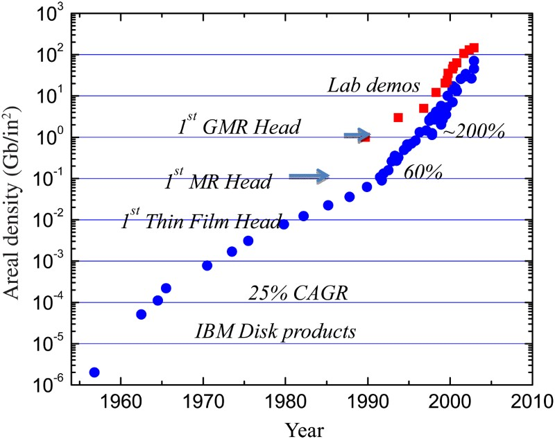
Hard drives to store data were first developed in the 1950s by IBM and the early hard drives used a rotating disk with magnetic tracks and a moving arm with the write/read head able to rapidly move from track to track as shown in Fig. 1. The write/read head, located at the end of the moving arm, consisted of small inductors that had a soft U-shaped magnetic core wrapped with a fine wire winding. Writing was done by passing a current through the winding such that a magnetic field would be generated at the poles that would magnetise a small section of the track. To read the information stored on the track, the inductor would be moved to the selected track on the rotating disk, and when the bit of information that was to be read was under the head the magnetic field generated by the bit would induce a current in the inductor coil and the direction of this current would indicate the direction of magnetisation of the selected bit, hence a ‘1’ or a ‘0’. The moving arm could move rapidly from track to track to enable the information to be stored and retrieved much faster than earlier storage media. Magnetic disk recording evolved in a similar way to computer logic, with better media enabling smaller bits and hence denser storage. However, as the media got better the write/read head had to shrink as well, and around 1980s the wire winding in the read/write head was replaced by a thin film inductor, and the read and write functions were separated. About 10 years later, the inductive reading was replaced by a magneto-resistive mechanism called anisotropic magnetoresistance (AMR). The resistance of an AMR film is different depending on the direction of current relative to the magnetisation, and the direction of magnetisation is sensitive to the field applied by the bits on the rotating disk. These AMR films could sense smaller fields than the inductive sensors used until then, and were the dominant technology until 1998 when IBM introduced the Travelstar series of hard drives that replaced the AMR sensors with the GMR spin valve developed by Stuart Parkin. This was indeed a disruptive change for the hard drive industry as it enabled a significant increase in density and IBM was able to leapfrog its competitors. The fact that this significant change occurred only 10 years after the discovery of GMR was presumably due to the fact that the magnetic storage industry was already familiar with magneto-resistive AMR sensors; the replacement of AMR with GMR sensors was straightforward, and instantaneously gave an order of magnitude improvement in the signal. All the magnetic hard drive manufacturers licensed this technology from IBM and GMR sensors became the new industry standard. Eventually, as the density of storage increased, the GMR sensors were replaced with MTJ sensors, enabling the magnetic storage industry to stay on its own version of ‘Moore’s Law’, i.e. exponential progress. This is schematically shown in Figs. 1 and 2. Schematic and evolution of GMR read head since 1996 (adapted from Spintronics lecture notes, Prof. Stu Wolf, UVA 2006, with thanks to Stuart Parkin) Areal density of HDD vs. Year (courtesy of Stuart Parkin)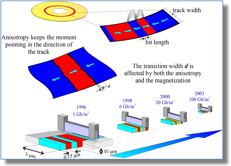
Magneto-resistive random access memory
The main focus of the DARPA SPINTRONICS project, started in 1996, was on MRAM since IBM was already well into the development of the GMR read head sensor. MRAM is based on the concept of using the direction of magnetisation of a free layer to store information, and the MR (variation in resistance with magnetisation) as information read-out. It was originally invented in the late 1980s when MRAM was developed to replace bulky and heavy plated wire radiation hard memories. 15 The basic memory cell was a dual stripe of AMR layers separated by a non-magnetic spacer. As described in the previous section, AMR materials were also used in the read head of magnetic recording hard disk drives (HDDs). AMR is a change in the resistance of ferromagnetic conductors depending on whether the magnetisation is parallel or perpendicular to the current. The magnitude of AMR is only about 2% for the most common magnetostriction-free NiFe or NiFeCo alloys suitable for device applications. The low resistance and low MR of metallic AMR thin film memory elements resulted in an AMR-MRAM memory architecture that required the connection of a large number of memory elements in series with a large pass transistor, hence the read signal was further degraded. MRAM was a niche non-volatile (i.e. retains memory when power is off) memory device for specialty radiation hard application when it was first invented, with dimensions larger than 1 μm.
The advancement of the MRAM technology benefited greatly from the rapid progress and revolutionary discoveries in magneto-resistive materials fuelled by the need to enhance magnetic recording areal density.
As described in the previous section, in the late 1980s, GMR was discovered. 2,3 It was immediately realised that this not only had the potential to enhance the performance of HDD, but also would improve MRAM read performance. The simplest form of GMR films consists of two magnetic layers separated by a Cu spacer, and had an MR ratio of 6% initially, and later more than 10% with improvements. New MRAM storage cells using spin valves 16 and pseudo-spin valves 17 were proposed. The memory states were defined by the magnetisation direction of the free layer being either parallel or anti-parallel to that of the pinned or hard magnetic layer. No magnetic fields were required during read operation for these new memory modes. However, the all-metallic thin films still required many elements to be connected in series with a pass transistor, which degraded the read signal and speed.
In the early 1990s, higher tunnel magneto-resistance (TMR) using an AlOx tunnel barrier was discovered in MTJ materials.
13,14
While many efforts were directed towards adapting MTJs for HDD read head applications for higher areal density, a few pioneering groups,
18,19
partially funded by DARPA, were pursuing MTJ materials for MRAM applications. The resistance of MTJs was easily tuneable by varying the tunnel barrier thickness to match the impedance of the semiconductor isolation devices, so it enabled for the first time an architecture consisting of one MTJ element and one transistor (1 T/1MTJ), as shown in Fig. 3. The MR of an MTJ (TMR ratio ∼45% for an AlOx barrier) was much higher than that of a GMR structure, and the read signal of MTJ-based MRAM was greatly improved as a result. A read speed in the range of 10 ns became feasible as a consequence of the improved signal levels. Schematic drawing for field writing MRAM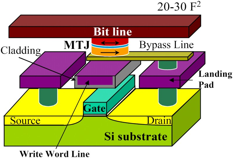
The writing was accomplished by flowing orthogonal currents to produce the required orthogonal magnetic fields at the cell at their point of crossing. The writing current per line was on the order of 5–10 mA or larger: a very large pass transistor was thus required to control the pulsing of this large current. The only feasible option to minimise memory chip footprint was to share this large write current over many rows or columns of cells. The bits at the cross-points got written, while the bits that experience half of the writing field under just one current line were ‘half-selected’. The magnetic switching fields of a single free layer depended sensitively on the cell edge properties, and had a large variation in a large memory array. As a result, some cells could experience half-select disturb switching problems. This was one of the key problems blocking the development of magnetic field writing MRAM memory products. The invention of a new field writing toggle mode using nearly balanced synthetic anti-ferromagnetic (SAF) free layers resulted in a rotational switching of the free layer with a greatly enhanced writing operational window and a very low upset probability. 20
An MRAM chip product prototype was announced in 2003 and the first ever MRAM commercial products started to ship in 2006. 21 The manufacturability of MTJ devices as memory bits was proven in these non-volatile MRAM memory products, having fast read and write speeds (10s of ns) with nearly unlimited endurance.
Today 180 and 90 nm standalone MRAM products are finding more and more applications in various areas where their unique features of being non-volatile, fast and of unlimited endurance are vital: these include satellite applications, automotive data recorders, industrial controls, etc. MRAM is currently being developed at 65 nm for both standalone and embedded applications.
Present
STT-MRAM
STT-MRAM stands for spin transfer torque MRAM. It utilises a spin polarised current to directly switch the magnetisation of a nanomagnet. It was theoretically predicted in 1996, and first demonstrated in metallic spin valve thin films with a critical switching current density (Jc0) >107–108 A cm−2, 22–27 that is too high for practical memory devices. MgO-based MTJs with a crystalline MgO(001) tunnel barrier were theoretically predicted to possess symmetry-enhanced spin polarisation, and exhibit MR ratios well above 1000% at room temperature. 28 Experimentally, giant TMR ratios of up to several hundred percent at room temperature have been demonstrated – first in epitaxial and textured MgO-based MTJs 29,30 and later in textured CoFeB/MgO/CoFeB MTJs. 31–33 A record TMR value of 604% at room temperature has been reported using a CoFeB/MgO/CoFeB MTJ. Breakthroughs in MgO-MTJs having enhanced spin polarisation and the resultant high TMR ratios along with lower STT switching current density played a pivotal role in boosting the performances of MgO-MTJ-based STT-MRAM. The scientific explanations for MgO symmetry-enhanced tunnelling and spin transfer torque switching have been extensively reviewed elsewhere. 9,33
The STT switching technique brings significant advantages to MRAM provided that the required switching current and voltage can be supplied by a minimum-sized isolation transistor device. STT-MRAM avoids the half-select disturb problem because the writing currents only flow to the cells being written. STT-MRAM enables MRAM scalability beyond 90 nm by reducing write current more than 10× in a 1-T (transistor)/1-MTJ memory cell architecture such as the one shown in Fig. 4 with a theoretical minimum cell size of 6 F2. It also leads to simpler memory architecture and manufacturing than conventional MRAM. STT-MRAM memory cell cross-sectional sketch. BL stands for Bit Line, SL stands for Sense Line and WL stands for Word Line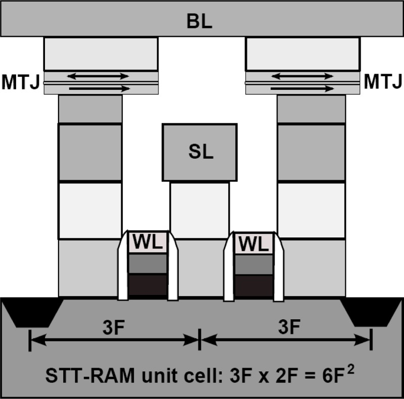
A viable new mainstream memory technology must demonstrate a clear path to migrate to smaller and denser memory size with lower power consumption as the underlying CMOS logic technology scales down as predicted by the international technology roadmap for semiconductors roadmap. One of the major drawbacks of conventional field writing MRAM has been the increase in switching current as the technology scales down. STT-MRAM solves this switching current problem by applying the spin polarised current vertically through the MTJ element. Whether the nanomagnet switches or not is related to the current density; therefore, as the CMOS technology scales down, and the area of the MTJ element decreases, the total current decreases, as shown in Fig. 5. Comparison of writing current scaling trends between field writing MRAM and STT-MRAM assuming low theoretical STT critical switching current density of 1 × 10⁶ A cm−2 (black curve) and 5 × 10⁶ A cm−2 (red curve)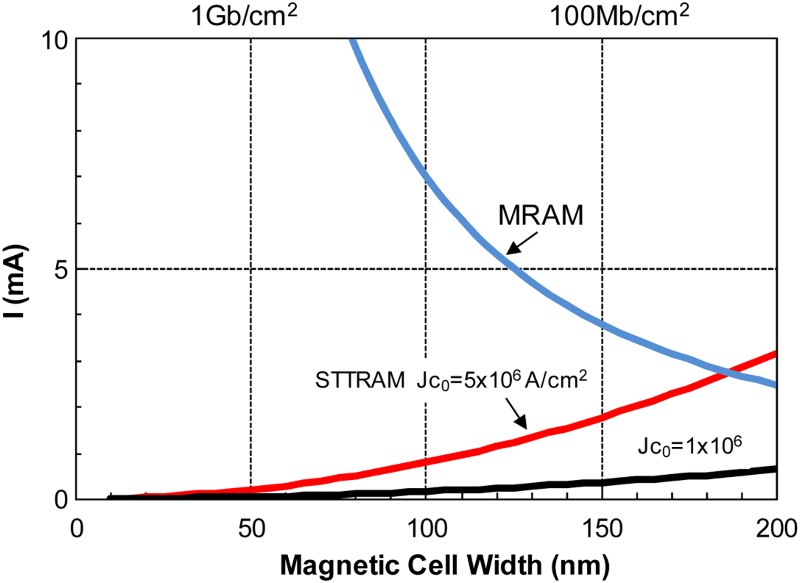
One of the key issues of STT-MRAM technology has always been the reduction in the STT writing current and voltage of the MTJ storage element while maintaining sufficient thermal stability for adequate data retention with tolerable write and read error rates. 34 Thermal stability of the storage layer in MTJs not only affects STT-MRAM memory cell stand-by data retention, it also affects the write current distribution, and write and read error rates. One key parameter of the STT writing mechanism is called the STT switching efficiency, defined as the ratio of the thermal stability factor (Δ) over the critical STT writing current Ic0 to compare various types of MTJ materials and devices. 35 Ic0 is the STT switching current linearly extrapolated to 1 ns from longer pulse-averaged switching currents. In a large array of MTJ cells, due to a combination of factors including distribution effects, spin precession caused increase in STT switching current faster than linear below 100 ns, and an overdrive of writing current necessary to achieve a write error rate (WER) below 1 × 10⁻⁶, a switching current two to three times the Ic0 value is needed to be delivered by the cell transistor for a fully functional STT-MRAM memory chip.
After the initial discovery of high TMR CoFeB/MgO/CoFeB MTJs 31,32 with in-plane magnetised thick (>2 nm) CoFeB layers, intense research efforts were carried out by groups around the world to achieve low resistance-area (RA) product and a high TMR value for magnetic recording read head application with a SAF coupled pinned layer for magnetic recording read head application. 36 The resulting in-plane MgO-MTJ stack provided a baseline starting point MTJ stack for studying STT switching properties targeting memory applications. Unlike the read head, where a linear response is desired as the free layer is rotated by a magnetic field from the recording media to be sensed, the STT-MRAM requires two distinct orientations of the free layer with an energy barrier of at least 60kBT between the two states. Naturally, the same type of magnetic shape anisotropy scheme for the storage layer or free layer that was used in field writing MRAM, was also adopted for STT-MRAM technology development by nearly all groups. In-plane STT-MRAM material and device optimisation for lowering Jc0 mostly has mainly focused on free layer CoFeB alloy composition, free layer composite layer stacks, capping layer choice and effects, insertion layer choice and effects etc.
To switch the free layer magnetisation of an in-plane MTJ device, a spin polarised current is applied, and the free layer magnetisation starts precessing around the direction of the total effective field. The magnetisation has to overcome a very large out-of-plane demagnetising field before it can switch to the opposite direction. The out-of-plane demagnetising field does not contribute to the thermal stability of the in-plane free layer, yet it causes the STT writing current to be high, thus making the ratio of writing current over Δ/Ic0 low. One promising approach discovered in solving the high out-of-plane demagnetising field of conventional in-plane MTJ devices is to induce strong perpendicular anisotropy in the in-plane free layer material through material engineering, to the degree that it nearly cancels the demagnetising field, so that the in-plane magnetisation of the free layer can easily rotate out of plane and switch to the opposite in-plane direction. 34 Shape anisotropy will still be needed to achieve adequate thermal stability.
Although it was thought that an in-plane MgO-MTJ could possibly scale down to below the 20 nm node by using a thick free layer and large aspect ratio, such an approach was contradicted by careful modelling and analysis 37 which combined the effects of decreasing demagnetisation as the STT-MRAM cell dimension shrinks to below the 20 nm node, and increasing interfacial anisotropy in the free layer induced by capping. This combination would force the magnetisation of the CoFeB layer to tilt out of plane, the conclusion being that it would be very difficult for in-plane STT-MRAM to scale below the 20 nm node. In the years that followed, most research groups have thus switched to work on perpendicular MgO-MTJ-based STT-MRAM for improved scalability prospect and higher STT switching efficiency.
STT switching comparison between early perpendicular MTJ and in-plane MTJ elements 39
STT switching comparison adapted from Ikeda et al. 44 (Session 4: Spin Transfer Torque Memory)
The STT switching efficiency (Δ/Ic0 ) value of nearly 1 for the first published I-PMA CoFeB free layer approached the best performance of the undisclosed L10 type free layer with a film damping constant (α) of 0.028 published in the 2008 IEDM. 38 Even better results were published in the 2012 IEDM by using yet another undisclosed free layer. 52 The undisclosed free layer was sandwiched by a dielectric seed layer and an MgO tunnel barrier, with a thickness of about 1.6 nm (estimated by the transmission electron microscope cross-sectional picture published). The damping constant of this free layer was reduced from 0.02 to 0.004. The free layer had a PMA HK value of 3000 Oe, and an MS of about 1250 emu/cc. The delta value (Δ) for a 30-nm circular device was about 61, and the parallel to anti-parallel (P2AP) Ic value at 3 ns was 30μA. The free layer Hk value was between 4000 and 8000 Oe. The estimated Ic0 value was 7–14 μA, the value of Jc0 was ∼1 to 2 MA cm−2, and the STT switching efficiency value was about 4–9. The DC Jc value was estimated to be about 0.5 MA cm−2. These parameters are among the best ever published for an undisclosed perpendicular material.
For a CoFeB-based free layer stack sandwiched between two optimised MgO layers, and in conjunction with device integration improvements, a high STT switching efficiency value of 5 was obtained in a 30 nm device with a TMR ratio of 150% at RA = 12 Ωμm2. 53 The device free layer damping constant was estimated to be 0.008. 54 The performance of published CoFeB-based free layer thus is approaching the best values published for an undisclosed perpendicular free layer material. 52
In summary, STT-MRAM device performance retains the major benefits of field writing MRAM of being a fast and non-volatile memory with no known wear-out mechanism, and unlimited endurance; and extends the scalability to sub-10 nm nodes.
The promise of STT-MRAM as a fast non-volatile memory has sparked many memory chip prototype demonstrations over the years. SONY Corporation demonstrated for the first time a 180 nm logic STT-MRAM test chip in 2005 at IEDM, 55 while Hitachi and Tohoku University demonstrated a circuit design for a 2Mb STT-MRAM chip in 2007 at ISSCC using a 200 nm CMOS process. 56 These early STT-MRAM demonstrations used large transistor nodes and smaller MTJ sizes (90 nm width), for their larger drive currents to switch a smaller MTJ element. Later, 50 nm perpendicular MTJ dots were reported to have very low STT writing current, 38 and a 45-nm CMOS platform was used for an embedded STT-MRAM test chip using in-plane MTJ films. 57 Devices as small as 20 and 17 nm were demonstrated. 58,59 For the first time, MTJ-based memory devices were being developed at the same advanced nodes as mainstream semiconductor memories.
Demonstration of a fully functional STT-MRAM memory chip is an important technology development milestone prior to customer sampling and product shipping. High performing critical parameters need to meet targets simultaneously in the same MTJ devices, and they need to remain the same in all MTJ devices. Key characteristics of a fully functional STT-MRAM chip reflect the reality and maturity of the STT-MRAM technology. The process of yielding one fully functional memory chip, and improving memory chip yields to above 90%, is a process of engineering trade-offs among all important device parameters. Techniques that boost one parameter of MTJ devices while degrading others cannot be simply used to yield fully functional memory chips. Therefore, fully functional chip metrics are what matters after all the engineering tradeoffs for yield enhancement. This is fundamentally different, and far more challenging, than developing individual magnetic recording single read head devices.
Demonstration of fully functional 8Mb STT-MRAM chips with perpendicular MTJ with sub-5 ns writing for non-volatile embedded memories was published in 2014. 65 The 8-Mb test vehicle was based on a 90 nm CMOS technology and used a 1 T/1MTJ cell architecture with a cell size of 50 F2 (F = 90 nm). MTJ bit size was 50 nm in diameter, the free layer was a CoFeB film sandwiched between two MgO layers, TMR ∼120%, RA ∼11 Ωμm2, R(low) ∼20 kΩ, Vc0 ∼170 mV. One-Mb chip WER was <1E-6 without any error correction circuit, with pulse width of 5 ns. The J c0 value was estimated to be ∼1.6 to 2.0 MA cm−2. The PMTJ used survived 400°C for 30 min processing. The same MTJ bits were projected to fit comfortably within a 28 nm CMOS 67 F2 cell in a well-established foundry process.
Currently, mainstream semiconductor memory technologies like SRAM, DRAM and Flash have been greatly challenged to scale for future generations. SRAM has high power consumption, and its leakage power increasing tenfold with each technology node. DRAM needs constant refreshing, its refresh current keeps increasing and it is becoming harder to maintain the minimum capacitance needed. Flash memory has limited endurance, high write power, very slow write speed; multi-level cell and aggressive scaling leads to reduced performance and a complicated controller. However, fuelled by explosive demands by mobile devices such as smart phones and tablets for RAMs and storage memory with faster speeds, cheaper costs and lower power consumption, novel solutions to extend the capabilities of existing memories have been invented and implemented in production for increased memory capacity, faster read and write speeds, and reduced power consumption. The success of pushing the scaling limit of existing memory technologies, especially for NAND-Flash and DRAM memories, provided the electronics components foundation necessary for the smart phone, mobile computing and cloud computing technological and societal lifestyle changes that we are all living through today. Thus STT-MRAM has to compete with a rapidly changing memory environment 58 and it will be a formidable challenge to replace any of them.
Based on the properties of the fully functional STT-MRAM memory chips demonstrated so far, STT-MRAM memory will be initially used alongside existing random access memory (RAM) memories and storage memory or hard drives, in boosting the speed performances of the total system, either as an embedded memory, or as a standalone memory module. Another application is where fast non-volatile storage with unlimited endurance is required, similar to the markets where toggle field writing MRAM chips are mainly being utilised today.
Significant material and device development work is further required to demonstrate STT-MRAM fully functional memory chips at a leading mainstream semiconductor memory technology node, and be considered as an alternative high-speed, non-volatile random access ‘working’ memory. The basic requirements for this ‘working’ memory are: the capability of operating at high read and write speeds of 10–30 ns, and having nearly unlimited endurance, low switching current, supplied by a minimum-sized transistor (6 F2 memory cell size) in a leading edge node. These capabilities have to be achieved along with high thermal stability, high TMR ratio and low RA, for all the MTJ devices in a large memory array, with a narrow distribution of values. Significant advances continue to be needed for STT-MRAM to fulfil its ‘Universal Memory’ potential.
Main alternative non-volatile memories pursued by industry include phase change memory (PRAM) and resistive change memory (RRAM). These not only lack the endurance required for a working memory, but also operate slower than the required 10–30 ns for both read and write operations. STT-MRAM has the potential to meet both the endurance and speed requirements as a working memory.
Memory technology performance comparison chart
As the STT-MRAM technology matures, and cell size is reduced to 4 F2 and below using cross-point architecture and multi-states per cell, STT-MRAM may also possibly be used as a replacement for storage class memory such as Flash.
Future
Spin-based logic
Modern CMOS-based logic devices use electronic charge to encode digital information (binary bits 0 and 1). Charge is a scalar quantity; therefore, logic levels must be distinguished by a difference in the magnitude of charge. The logic operations invariably involve electric charge flows and associated Joule dissipations that are unavoidable in any charge-based electronics.
Spin is a pseudo-vector that has a fixed magnitude, but a variable direction (or polarisation). The spin of an electron is bistable in a magnetic field. These two spin polarisations can encode the logic bit ’0’ and ‘1’. Switching between logic levels can reduce energy dissipation significantly since the I2R loss is eliminated. The energy dissipated during a spin flip (logic switching event) is the energy difference between the two bistable polarisation states. This energy can be made less than the thermal energy kT without causing too many unwanted random spin flips and bit errors. It has been predicted that the energy dissipated during a spin switching event can be less than the Landauer–Shannon limit of kTln(1/p). 66,67
There are several spin-based logic circuit styles that have been proposed and developed that are intrinsically non-volatile, and dissipate low power. Here we briefly review a few such spin logic concepts. It should be noted though that there are many challenges for the practical implementation of spin logic especially those related to the clock speed, I/O and the control of the magnetism via the electric means.
Magnetic quantum cellular automata
The magnetic quantum cellular automata (MQCA) is a spin version of the quantum cellular automata (QCA), initially proposed by Tougawa and Lent 68 at the University of Notre Dame. A QCA cell has been demonstrated first based on Coulomb interactions of confined electrons in quantum dots in 1997 69 followed by a demonstration of a QCA logic gate. 70 However, the logic operations by QCA were only feasible at subKelvin temperatures due to the weak strength of the Coulomb interactions.
MQCAon the other hand are operated based on the exchange interactions of spins instead of charges. The exchange interaction among spins inside one ferromagnetic dot can transform the dot (∼100 nm) into one single classical spin which then can be coded as ‘0’ or ‘1’ based on the spin direction, e.g. up vs. down. Cowburn and Welland
71
have first demonstrated room temperature MQCA using a chain of ferromagnetic circular dots. Later, the group at Notre Dame developed an MQCA using non-circular dots and demonstrated magnetic switching of MQCA wires with the assistance of an external magnetic field (the clocking field).
72
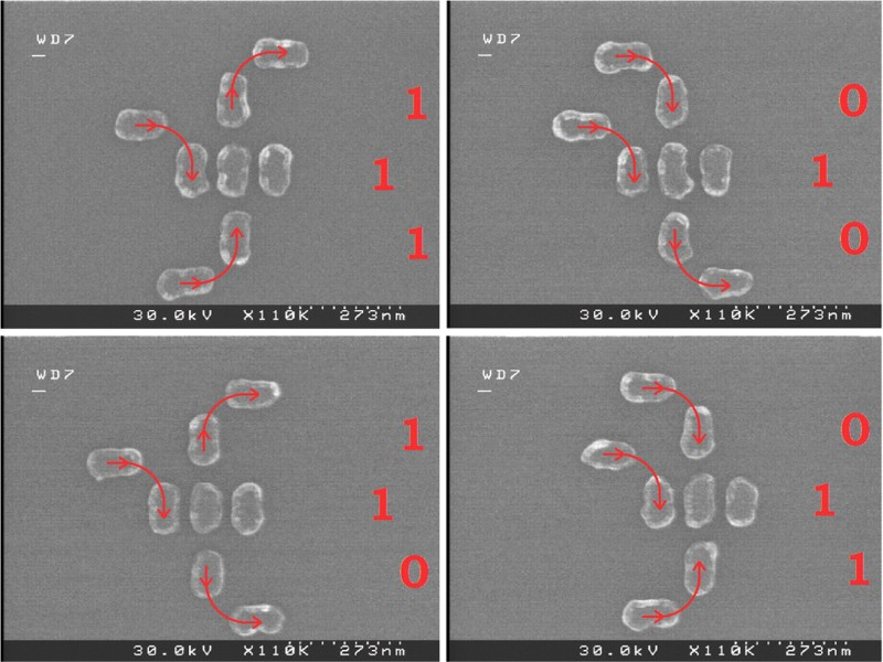
Subsequently a logic gate based on the majority voting function has been also demonstrated in 2006 as shown in Fig. 6.
73
Similar to the QCA, the switching between the ground states in MQCA is adiabatic. The clocking field helps to align the magnetisation along the hard axis of MQCA dots and, once it is removed, the spins in the dots relax into the ground state set by the initial input without falling into metastable states. SEM image of majority gates composed by magnetic dots. The arrows indicated the magnetisation direction due to an applied external field. The ‘down’ magnetisation of the bit is assigned ‘0’, and the opposite as ‘1’ (adapted from Imre et al.
73
)
The scaling of MQCA is limited by the superparamagnetism limit at which the ferromagnetic dots become superparamagnetic. This critical size can be as small as 2 nm, and is strongly dependent on the magnetism of the materials. It is worth noting that the spin state can be maintained over ∼1 mS even below the superparamagnetism limit, which is often sufficient for information processing at GHz clock speeds. 74
The MQCA is inherently non-volatile and with low energy dissipation, which extends the functionality and reduces the energy consumption at the same time. However, MQCA raises some challenges on the performance and the design. Particularly, it lacks an efficient and compact design for the input/output interface between MQCA and the conventional integrated circuits owning to the translation between the charge and spin, as discussed by Orlov et al. 75
Reconfigurable array of magnetic automata
Reconfigurable array of magnetic automata (RAMA) has been proposed by Wolf et al., 76 which was based on the discovery of the magneto-elastic coupling in multiferroic nanocomposites. The ferroelectric perovskite and a ferrimagnetic spinel can self-assemble in a structure in which magnetic pillars are epitaxially embedded in a ferroelectric matrix. 77 In these multiferroic composites, the magnetisation direction in the pillars can be reoriented through the application of an electric field to the ferroelectric matrix thanks to the magneto-elastic coupling via vertical interfaces, which has already been demonstrated on CoFe2O4 pillars embedded in a ferroelectric BiFeO3. 78
The proposed magnetic logic array is similar to MQCA. With the array of the ferromagnetic pillars, the adjacent pairs of pillars couple anti-ferromagnetically through their dipolar exchange. Similar to QCA, each bit consists of four pillars in a square with two corners polarised up and two down, as illustrated in Fig. 7. The two states of this bit can be represented by the state of the left uppermost corner, which could be up or down and the other magnets would adjust accordingly. The RAMA consists of a square array of magnetic pillars that are embedded in the ferroelectric matrix. There are crossbars above and below the matrix that are used to apply an electric field on any selected pillars. Schematics of the four pillar bit pattern and the RAMA logic array
76
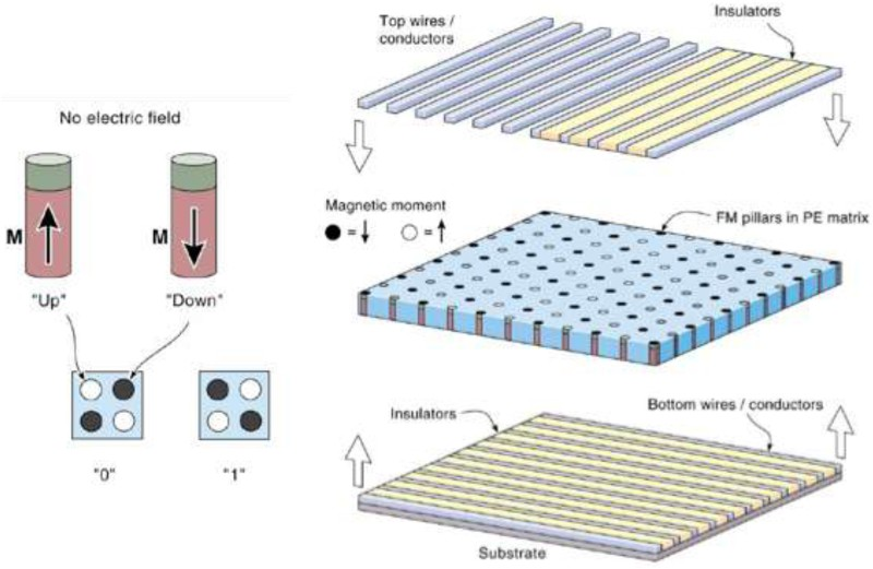
The array can be configured into different ‘gates’ by using the interaction of the ferromagnetic pillars with the ferroelectric matrix and the sole use of electric fields for configuration, input, output and operation of the array. A gate pattern can then be formed in the array by rotating the magnetisation of all unnecessary pillars from out-of-plane to in-plane, therefore, removing the magnetic dipole coupling between the adjacent pillars. To reconfigure the array, a reverse electric field needs to be used to rotate the magnetisation of selected pillars back to out-of-plane to form a new logic gate pattern as described by Wolf et al. 76
These arrays of magnetic pillars can function well as large memory arrays since the bits are non-volatile and can be individually addressed. In fact, it can provide a very dense array of non-volatile random access memory if the pillars are densely packed.
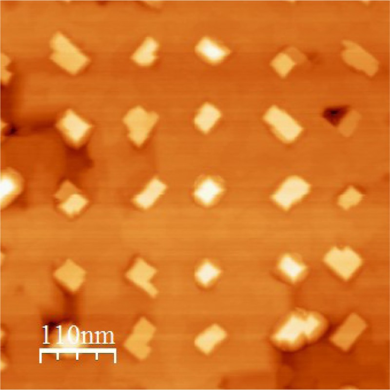
Controlling the locations of the pillars in self-assembled composites is essential for RAMA. Patterning processes have been developed to template the positions of CFO pillars in the epitaxial CFO-BFO nanocomposites by several groups.
79–81
The AFM image of such a patterned nanocomposite with a square array of CFO pillars with a pitch of 100 nm is shown in Fig. 8. The microstructure and the physical properties of the nanocomposites were characterised, and it showed that these films were epitaxial with excellent quality.
79
Transpinnor
A transpinnor, a less known logic devices based on giant magneto-resistive structures such as spin valves, has been proposed and demonstrated by Barna et al. 82 The basic transpinnor device consists of a bridge of four spin valves and a current strip line that could exert magnetic fields on the spin valves. The spin valve is used for the output, and the strip line is connected to the input signals. In the initial stage the bridge is balanced; therefore, there is no output. When an ‘input’ current passes the strip line, an external H field is generated. If the spin valve is switched to a different resistance state by the external magnetic field, an output signal is generated since the bridge is no longer balanced. If two current strip lines are used for a single transpinnor, the transpinnor can be used as a logic gate for different logic operations.
Applications for transpinnors include amplifiers, memories, A–D converters etc. However, there are some challenges that limit the interests and the advancement for transpinnors. First, it is difficult to scale the transpinnors because of the size of the bridge and the strip lines. Also the output signal is very small due to the small GMR (typically <10%). It has been proposed to use MTJs (TMR >100%) to replace spin valves to improve the magnitude of the output, but this would still not resolve the scaling issues.
Josephson magnetic random access memory
Rapid single flux quantum (RSFQ) logic is the latest generation of high performance superconducting computer based on Josephson junctions. RSFQ can have clock rates in excess of 100 GHz and with dramatically reduced power requirements. These features provide an opportunity to build compact, multi-petaflops systems to meet the needs for high performance computing (HPC). 83 However, the lack of cryogenic high capacity memory technology with the matching clock speed and ultra-low power dissipation is a roadblock to the implementation of RSFQ logic for HPC. 83,84
Superconducting memory cells based on superconducting quantum interference devices have been developed. The magnetic flux threading a superconducting loop is used to provide the physical basis for a digital memory element. 83 Despite the efforts to develop a high-capability superconducting memory, only a 4-kbit RAM has been demonstrated. 85 The superconducting loop requires large cell sizes, which makes the superconducting memory cells difficult to scale, thus the smallest cell was 15 μm × 15 μm. In addition, the superconducting memory cell consumes too much energy since it uses a less energy-efficient RSFQ technology. Significant improvements in the cell size and power dissipation is required for the superconducting memory to be a viable option for HPC. 83 Conventional semiconductor memories, specifically designed for cryogenic operation, can be integrated with superconducting logic circuits, and such hybrid memory technology is capable of higher capability than the superconducting memory. 64 kbit hybrid Josephson-CMOS memory chips have been demonstrated. 86,87 However, the power and energy dissipation of the hybrid memory is still too high for exascale superconducting computers. 83
A cryogenic RAM based on the magnetic Josephson junction (MJJ) was conceived in the 1990s, 88–92 and the experimental demonstration of MJJs in 1999 led to increased attention to this concept and recently prompted an investigation of the idea of a superconducting-ferromagnetic hybrid RAM. 93–98 The name ‘Josephson magnetic random access memory’ (JMRAM) was from a patent filed by Herr and Herr 92 at Northrop Grumman in 2011.
The operation principles of these JMRAM are based on the effect of the magnetisation on the magnitude and the phase of superconducting currents through the junction. Instead of the resistance value as in MRAM, the logic ‘0’ and ‘1’ in JMRAM can be defined either by different values of the critical current and/or the phase of the current through the hybrid structure.
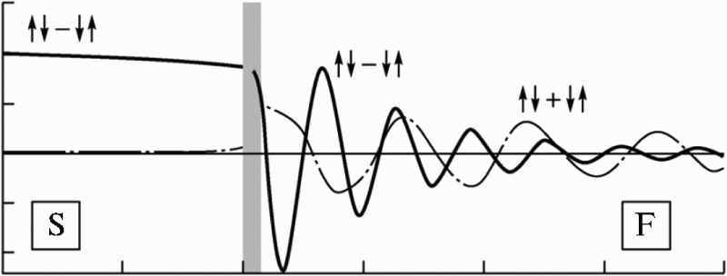
Figure 9 illustrates the amplitude and probability functions of singlet and triplet Cooper pairs in the vicinity of a superconductor (S)/ferromagnet (F), an SF interface. The dissipation-free super-current in superconductors is carried by Cooper pairs formed by two electrons. Typically, a Cooper pair is in a singlet state since the two electrons possess opposite spins. The presence of an external magnetic field tends to break up the Cooper pairs since the spins of the electrons prefer to align with the magnetisation direction. Thus, in a ferromagnetic material, the super current is diminished as the internal magnetic field destroys Cooper pairs. The coherence length of Cooper pairs in ferromagnetic materials is typically much shorter than that in normal metals. The amplitude of the super current decreases exponentially into the ferromagnetic layer. In addition, the phase of the super current experiences an oscillatory change. As a result, the phase of the super current referred to the electrodes can reverse sign and be either positive (denoted ‘0’) or negative (denoted ‘π’) as a function of the thickness of the ferromagnetic layer in the S/F hybrid structures. Amplitude and probability functions of singlet and triplet Cooper pairs in the vicinity of a superconductor (S)/ferromagnet (F) interface (adapted from Bakurskiy et al.
99
)
Experimentally, the effects of the magnetic field on the super current have been demonstrated in SFS junctions for strong and weak magnetic materials.
100–105
The fast decay, as well as the oscillation in the critical currents as a function of the thickness of the magnetic layer (Co and PdNi), has been observed as shown in Fig. 10. At certain thickness values, the critical current dropped to zero due to the 0–π transition in the phase. The rate of decay and the value of the first critical thickness are strongly dependent on the magnetisation as well as the coherence length of Cooper pairs in the ferromagnets. The first critical point occurred at a ∼2.5 nm thickness in SFS junctions with a Co ferromagnetic film. For a weaker ferromagnet like PdNi, the first critical thickness was as large as ∼35 nm.
105
It is also worth noting that the presence of a so-called ‘dead layer’ in the magnetic films often causes a large distribution in the values of the critical thickness for the 0–π transition.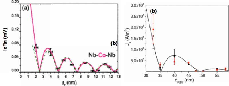
Many different JMRAM structures have been proposed, with one or two ferromagnetic layers embedded in Josephson junctions. Recently, an MJJ with two ferromagnetic layers has been used to demonstrate the basic switching memory operation based on the relative alignment between the two magnets.
98,99,103
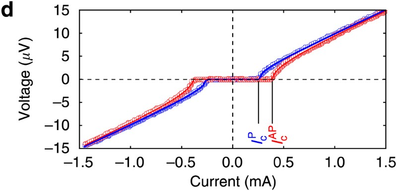
The operation of a spin valve-based MJJ is analogous to the spin valve or MTJ, but instead of the resistance, the magnetisation states dictate the phase and the magnitude of the super-current through the junctions. Figure 11 illustrates one such MJJ and its possible operation mode. When the spin valve is in the ‘P’ (parallel) state, the effective thickness of the two magnetic layers is equal to the critical thickness of the ferromagnets for the 0–π transition. This state yields a near zero JC
as shown in Fig. 11. In contrast, for the ‘AP’ (anti-parallel) state, the effective thickness becomes much smaller than the critical thickness because the total magnetic moment that the super current encounters in the MJJ is reduced. Thus JC
becomes much larger as compared to that in ‘P’ state. This principle has been demonstrated despite the fact that the change in JC
was relatively small as shown in Fig. 12.
95,98,103
Schematic of a Josephson junction with an embedded spin valve. NM stands for the normal metal, typically a Cu spacing layer. The critical current of this JJ is a function of the magnetisation configuration of the two magnetic layers I–V of the spin-based MJJ measured at the magnetic field giving the peak Im for P and AP states at 4 K (adapted from Baek et al.
98
)
In summary, a JMRAM consists of Josephson junctions that have embedded ferromagnetic layers as the tunnel barriers (or weak links) that demonstrate the features of memory elements at cryogenic temperatures. The operation of such a JMRAM relies on the effect of the total magnetisation on the super current and on the phase of the super current relative to the superconducting electrodes. The performance of JMRAM relies on the selection of magnetic layers that, ideally, require very minimal energy to switch and also possess a relatively large coherence length for Cooper pairs.
Spin-torque nano-oscillators and their applications
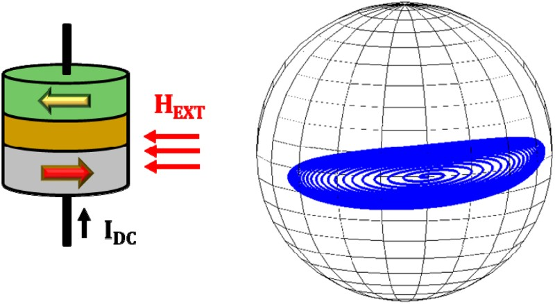
Just as in STT-MRAM, the spin torque nano-oscillator (STNO) device relies on the spin transfer torque effect as the driving force of its operation. Unlike the STT-MRAM, however, the spin transfer torque effect generates a sustained precession in the magnetisation instead of a complete reversal of the free layer (Fig. 13).
a Structure of a MTJ with a fixed layer, whose magnetisation is pinned, and a free layer whose magnetisation can be changed. b The stable precession trajectory of the magnetisation of an in-plane free layer in response to spin transfer torque
116
The first theoretical work on oscillations within magnetic films was done by Slonczewski, 22 who showed that a torque can be applied to a magnetic thin film via spin-polarised currents. Normally, perturbations caused by applied torques quickly dissipate within the magnetic film because of various scattering effects, which creates an effective damping field for oscillations. 107 However, in certain configurations, torques generated by spin-polarised currents can reduce and even cancel out the damping field, yielding sustained precessions in the magnetic thin film.
Soon after the theoretical development, indirect evidence of oscillations in Co/Cu/Co spin valve was demonstrated experimentally. 24 In addition, the experiment showed that the frequency of oscillation can be controlled by the magnitude of the spin polarisation current. Direct experimental observation of microwave oscillations 108 and spin waves 109 not only validated the theoretical predictions, but also showed a variety of dynamical modes of oscillations depending on the device geometry and orientations of the applied magnetic and electric fields. These microwave oscillations generated by the STNOs exhibit wide ranging tunability by adjusting the DC current and applied magnetic field, with frequencies ranging from 0.1 to 100 GHz and linewidths on the order of ∼100 MHz. 110 More recently, it has been experimentally shown that two STNOs can mutually phase-lock and synchronise. 111,112 These experiments involved two MTJ structures with a shared free layer that allowed current injected spinwaves to interact with each other causing them to phase-lock. The ability of spin-torque oscillators to synchronise is not only advantageous in increasing the output oscillation power 113 but also provides a way of transferring information and computing with multiple oscillators.
While phase locking via magnetic spinwaves has been shown between two spin-torque oscillators, it still remains unclear whether this process can be scaled for fabrication, or even synchronisation, when many STNOs are involved. 114 In addition, spinwave coupling can only occur over short distances that will limit the types of connection topologies that can be achieved – and thus the types of possible applications.
A different coupling scheme based on electrically connected interacting STNOs has been considered in several studies. 115–117 As the magnetisation of the STNO precesses, the MR effect between the polarising and free layer create an oscillating electrical signal. Therefore, two (or more) STNOs can interact with each other through an electric connection that could lead to synchronisation. Electrically connected STNOs provide other advantages as well. First, each STNO can be independent of the rest of the system since specialised features, such as a shared free layer, are no longer necessary. Furthermore, electrical connections facilitate integration of STNOs with other passive and active circuit elements. This greatly expands the potential applications for STNO and opens the possibility of hybrid MOSFET/STNO devices.
However, when considering electrical synchronisation, not all STNOs are created equal. Variations in the STNO structure can yield very different magnetic precessions and output signals. As with STT-MRAM, PMA materials are attracting a great deal of interest especially for generating oscillations requiring small or zero applied magnetic fields.
118
One such configuration uses a hybrid structure with an in-plane free layer and an out-of-plane hard layer. Since the magnetisations between the two layers are on different axes, the oscillation path created by the free layer ensures that spin-torque is maintained for a larger range of motion. Therefore, the hybrid structure is capable of creating frequencies ranging up to 100 GHz. In addition, the TMR signals for the hybrid structure are stronger than those of the in-plane STNOs because, on average, the precession of the free layer creates a larger angle difference with hard layer. The oscillations produced by the hybrid structure are more complicated than those of the in-plane STNOs and they introduce additional frequencies to the signal (see Fig. 14
a).
a A hybrid STNO structure with an out-of-plane hard layer and an in-plane free layer. This configuration allows for a larger range of frequencies and also creates a larger TMR effect due to the large intrinsic angle difference between the two layers. The trajectory of the free layer for hybrid structures is complicated and trace out various Lissajous curves which have nonharmonic oscillations. b A DMTJ structure. The free layer of this structure oscillates in a circular, harmonic manner. The additional analyser layer can be used to create a larger TMR effect to read the magnetisation state of the free layer.116
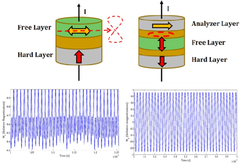
In addition to changing the orientation of the ferromagnetic layer, it is also possible to create additional layers, which can add increased functionality to the MTJ structure. In dual MTJs (DMTJ), another hard layer is placed on top of the free layer that can act as an analyser layer (see Fig. 14 b). This additional layer gives the device more flexibility since the bottom two out-of-plane creates harmonic oscillations while the top analyser layer is placed in-plane to create a large TMR signal for the read-out. This structure can have other functions as well, such as using anti-parallel hard layers to create symmetric switching in MRAM bit cell by simply reversing the direction of the injection current. These new possibilities make the DMTJ an active area of research for new applications. 119
One of the flexibilities of an electrically based coupling mechanism is the possibility of many different connection topologies. One promising topology is the parallel-connected STNO circuit. In addition to its simple design, it also allows multiple oscillators to interact with each other at the same time through a global transmission line. Furthermore, it can be shown that the parallel-connected STNO is a type of oscillatory neural network proposed by Hoppensteadt and Izhikevich 120 Oscillatory neural networks are ubiquitous in nature and provide the basis for many non-Boolean computational applications such as pattern recognition.
Furthermore, the oscillatory neural network model provides the theoretical basis for the conditions under which the parallel-connected STNOs synchronise. In the Hoppensteadt model, there is a global periodic signal that is the amalgam of all the oscillator signals, thus creating a conduit for the oscillators to interact with one other. In the parallel-connected STNO, this is done through shared electrical transmission line that connects all the oscillators and also acts to sum up all the signals to create the global periodic signal. The analog of the feedback mechanism of the Hoppensteadt model is the spin-torque interaction that occurs between the STNOs as a result of this global signal. Finally, the phase adjustments are an intrinsic property of STNO, thereby completing the requirement of the oscillatory neural network.
It can be shown through circuit analysis of the parallel-connected STNO that the frequency shift in each of the individual STNOs obeys the formula
An array of parallel-connected STNOs can be utilised as a pattern recognition device. Depending on the level of match between the two images, the current through the branch is altered leading to different frequencies, which act in a similar manner to the oscillatory neural network. Those branches with similar matches tend to cohere to a single frequency giving us a measure of the match between an input and test image – with large output power being high matching and small output power equalling low matching. The synchronisation of these signals is achieved between 10 and 20 ns. These bands represent the degrees of matching that are present in the array. If the amplitude of the oscillation signals is analysed, then the input signal with the highest degree match can be determined.
One of the most promising aspects of the STNO devices is the possible system-on-chip applications. 122,123 The nanoscale dimensions, coupled with the possibility of CMOS integration, low power, tuneable frequency through magnetic fields and electrical currents, high quality factor (Q >1000) and the possible control of coupling open many possibilities beyond the current state-of-the-art RF systems.
One such RF application are filters which take advantage of injection locking which has already been observed in STNOs. 124 Using a current mirror, we can create a circuit that allows the STNO to be tuned to a resonant frequency, and then apply an AC signal to the oscillator. For frequencies close to the filter frequency, the STNO acts as either a bandpass or a band-reject filter depending on the circuit topology used. This allows us to do signal processing for a wide range of frequencies (1–100 GHz). This simple circuit acts as notch bandpass/bandstop filter with line widths of ∼10 MHz.
Although the STNOs can be used to filter narrow bandwidth signals, we are interested in developing more robust techniques to tune the filter strength and bandwidth. One of the ways to increase the filter strength is to improve the current mirror design used to set the STNO resonance oscillation. Moreover, the filter strength can be increased via STNO synchronisation. It has been shown that the oscillation power of the STNOs can be increased through the synchronisation of multiple nano-oscillators. 113,116,125 However, the increase in strength begins to level out with more STNO since the oscillation power increases quadratically.
There are other applications which are actively being researched. 126 Because spin-torque devices exhibit an intrinsic instability leading to oscillation, these devices may also be exploited to realise self-oscillating RF mixers. Mixers are the central component of heterodyne receivers, which are the most important sensor architecture used for RF applications. Heterodyne receivers typically make use of a separate local oscillator with which the signal to be detected is mixed. This allows the power of the detected signal to be measured while maintaining phase coherence. STNO devices offer a means of realising self-oscillating mixers because the magnetic procession in these devices is inherently nonlinear. With the self-mixing characteristic of the device, the oscillation source and the mixer are combined in one device. In addition, the device is tuneable via applied current or magnetic field. All these advantages make STNO device an intriguing choice for realising RF/millimeter-wave tuneable mixers.
Summary and outlook
Spintronics has emerged in the last two decades as both an extremely fruitful direction of research into the properties and usefulness of the spin degree of freedom of the electron as it can apply to the exponentially expanding world of electronics. Despite the fact that spintronics is not a household word it has infiltrated almost every household in the form of the read head sensors for the hard drives that inhabit every desktop and most laptop computers. Embedded MRAM and in-plane STT-MRAM, are rapidly replacing SRAM in a host of applications that do not require ultra-dense memories. Soon these embedded spintronic memories will permeate the cell phone market because they are denser than SRAM, offer lower power at only slightly lower speed and are non-volatile.
Much of the present work in spintronics at most of the mainstream semiconductor companies and foundries is focused on the development of perpendicular STT-MRAM. The goal is a universal memory that can compete with the mainstream memories and surpass them in several key metrics as pointed out in Table 4. Although there are still significant challenges, the promise is worth the perseverance.
The future is where the sky is the limit. This review focuses on several innovative ideas where spintronics may have an impact because of the uniqueness of the approach. For example, nanomagnetic logic and storage may offer extremely high densities at very low power. Spin-torque oscillators are a very novel approach to pattern recognition that may be relevant for handling massive data sets. Almost every day we are learning more about the nature of the ‘quantum’ spin and (even though it has not been reviewed in this article) the spin of the electron may be the critical path for quantum computation or communication, another revolutionary change in how we process information.