
Abstract
Perovskite solar cells are promising candidates for next-generation photovoltaic devices with certified power-conversion efficiency for single-junction perovskite-based devices exceeded 25%. However, it remains challenging to fabricate a large-area and dense perovskite film using solution-based deposition methods. This is due to perovskite wet films being highly sensitive and unstable, and thus having only a narrow processing window. There is therefore a demand for ways to expand the processing window in the fabrication of perovskite films. Herein, we systematically review research on the role of precursor solutions and antisolvents during the perovskite formation process, and reveal the fundamental factors governing the width of the perovskite film-processing window. Then, we give an overview of current strategies for enlarging the processing window, which includes solvent and antisolvent engineering strategies. We conclude by summarizing current challenges in the development of perovskite solar modules with a wide processing window and provide perspectives for future development.
Introduction
Organic–inorganic hybrid perovskite solar cells (PSCs), which have the chemical formula APbX3 (where A is an organic or inorganic cation, such as CH3NH3 + (methyl ammonium; MA+), HC(NH2)2 + (formamidinium; FA+), or cesium (Cs+), and X is a halide ion, such as chloride (Cl−), bromide (Br−), iodide (I−), or their mixture) [1–6], have been widely investigated as promising candidates for next-generation photovoltaic devices due to dramatic improvements in their performance during the past decade [7–10]. For example, the best certified power-conversion efficiency (PCE) of single-junction small-area PSCs has exceeded 25% [11] within the past few years, which is comparable to the PCEs of state-of-the-art thin-film photovoltaic devices [12–14]. This rapid improvement in efficiency is largely a result of the excellent properties of perovskite materials, such as their high absorption coefficients, large carrier-diffusion lengths (>1 μm), low exciton-binding energies, flexible bandgap turnabilities, high defect tolerance, and ease of solution-based fabrication [15–21]. This enables perovskite materials to be fabricated into high-quality perovskite films with full coverage, smooth surfaces, large grains, and extensive crystallization, and thereby function as well-performing PSCs. Various methods have been developed to fabricate high-quality perovskite films to obtain highly efficient PSCs, including one-/two-step methods [22–24], vacuum-assisted deposition [25–27], dual-source co-evaporation [28–31], and vapour-assisted processes [32–34]. In addition, one-step antisolvent-assisted solution fabrication strategies have been widely adopted, as they are a particularly effective means of obtaining dense and highly crystalline perovskite films [35–37], which are crucial for a good device performance. In these strategies, the antisolvent extracts solute from the precursor, which generates a driving force for the formation of an intermediate phase [24,38,39]. However, perovskite film-processing windows with commonly used antisolvents, such as chlorobenzene (CB) [40–42], toluene (TL) [43], and diethyl ether (DE) [44], are extremely narrow, for two reasons. (1) The volume ratio of dimethylformamide (DMF)/dimethyl sulfoxide (DMSO) in the precursor solution must be precisely optimized within a narrow range for each antisolvent. For example, the DMF/DMSO volume ratios for CB, TL, and DE are 4:1 [45], 7:3 [24], and 9:1 [46], respectively; (2) Antisolvents must be added in a specific and short time period (8-10th s) after the processing begins, as otherwise the obtained perovskite film will have poor morphology, i.e. high roughness, a high density of pinholes, and low coverage. This extremely narrow processing window severely curtails the reproducible fabrication of large-area and efficient PSCs [47,48].
Although some efforts have been made to widen the processing window in perovskite film-forming processes via solvent engineering or antisolvent engineering, few researchers have examined the mechanisms responsible for the extremely narrow processing window or the fundamental interactions of solvents and antisolvents. Thus, there is a lack of understanding of the role of solvents and antisolvents in these processes. We address this problem in this systematic review. First, we examine research to determine what appear to be the key factors that influence the width of perovskite film-processing windows, and we summarize recent strategies that have been developed for widening these processing windows. We then detail the various strategies that are currently used for widening processing windows in the traditional one-/two-step method for fabricating perovskite films, which involve solvent engineering (such as precursor additives and solvent replacements), antisolvent engineering (such as mixed antisolvents and new antisolvents), and other methods. We conclude by giving an overview of the challenges and opportunities for the future development of large-area perovskite solar modules with wide processing windows.
The role of solvents and antisolvents
Nucleation and growth dynamic mechanism
Various solution-based fabrication methods have been developed for the fabrication of high-quality perovskite films, such as one-step spin-coating [49–51], slot-die coating [52–54], blade-coating [48,55,56], and inkjet printing [57–59]. A perovskite film is formed by the precipitation of a perovskite solute from a precursor solution, and thus the characteristics of the solvent used, such as its boiling point, vapour pressure, polarity, and viscosity, determine the effectiveness of the perovskite film-forming process and the quality of the final film [25,29,60,61]. In particular, solvents that are insufficiently or excessively volatile lead to perovskite films with poor morphologies and thus inferior optoelectronic properties.
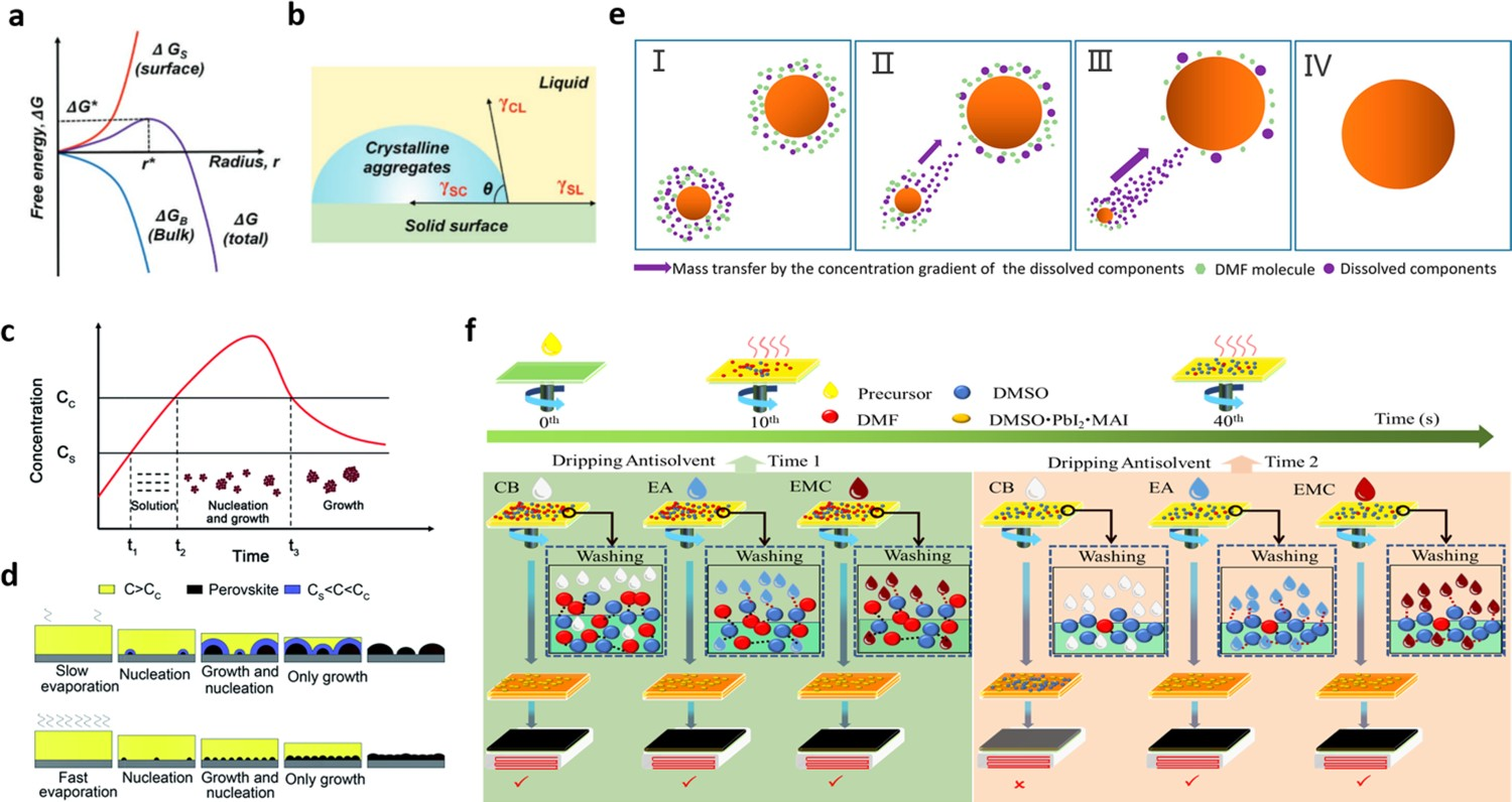
In general, the formation of perovskite films begins with nucleation. The nucleation takes place once the solute concentration sufficiently exceeds its solubility, which is defined as the supersaturated state. Currently, there are two major pathways in nucleation: homogeneous nucleation and heterogeneous nucleation. For homogeneous nucleation, the nucleation process happens without the need for preferred nucleation sites. The total free energy (ΔG) of spherical nanoparticle is the sum of the surface free energy (ΔG
s) and bulk-free energy (ΔG
B) and is expressed by the following equation: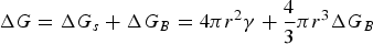
The curves corresponding to the above three parameters (e.g. ΔG, ΔG
B, and ΔG
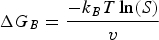
S are shown in Figure 1(a). If the nuclei have radii smaller than the critical radius (r*), they dissolved back into the solution. However, when nuclei radii are bigger than r*, the nuclei are thermodynamically stable and able to grow further. For heterogeneous nucleation, nuclei are generated preferentially in certain areas, such as defects, substrate, bubbles, or impurities, which is much more likely to occur than homogeneous nucleation process in real-world experiments. As shown in Figure 1(b), when the liquid is in contact with the substrate, it cannot maintain the spherical feature. Then, the surface energy between solid and liquid, solid, and crystalline aggregates, and crystalline aggregates and liquid are defined as (a) Profiles of free energy changes as a function of particle radius r for homogeneous nucleation: ΔG
B, ΔG
S, ΔG, ΔG*, and r* represent the bulk-free energy, surface free energy, total free energy change, critical free energy for nucleation, and critical radius of the nucleus. (b) Schematic illustration of contact angle (θ) for heterogeneous nucleation. Both images reprinted from [62] with permission. (c) A LaMer graph, which depicts the change in the concentration of a perovskite precursor solution as a function of time at a constant solvent evaporation rate. (d) Model of the nucleation/growth competition of perovskite crystals formed from a precursor solution under two different conditions: slow solvent evaporation and fast solvent evaporation, where C
C is the critical concentration and C
S is the saturation concentration. Both (c) and (d) images reprinted from [63] with permission. (e) Schematic diagram of the Ostwald ripening model. Image reprinted from [61] with permission. (f) Scheme of an antisolvent-assisted spin-coating process, illustrating the reason for the narrow processing window. Image reprinted from [64] with permission.


where the correction facto r(φ) can be expressed as follow:
For the growth of stable nuclei, there are two major mechanisms: surface reaction and monomer's diffusion to the surface. [66] Fick's first law [67], as shown in Equation (6), is introduced to explore the monomer diffusion mechanism, where J, r, D, and C represent the total flux of monomers coming in throughout the surface, particle radius, diffusion coefficient, and concentration at position x respectively [68].
For the growth process of nanocrystals in the solution state, Equation (6) could be changed to Equation (7) as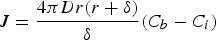


Given that monomer total flux J is a constant regardless of distance due to the steady state of the diffusion process of the growth species, Equation (7) can be rewritten as follows:

From Equations (8) and (9), it is obvious that there are two major factors limiting the crystal growth process: (1) the diffusion process of monomers toward the surface and (2) the rate of the reaction speed of these growth species at the surface.
Apart from the thermodynamical aspect to discuss the nucleation process, the LaMer model is also typically used in solvent engineering studies to probe the nucleation and growth processes of perovskites and thereby determine how they influence the morphology of perovskite films [60,63]. As shown in Figure 1(c), a LaMer curve characterizes crystallization as a three-stage process [63,69,60,70]: (I) solution; (II) nucleation/growth; and (III) crystal growth. In (I), the solute is completely dissolved in the solvent, and thus no nuclei form in the unsaturated solution due to the high energy barrier to spontaneous nucleation. In (II), some colloidal solutes gather together, resulting in the formation of some nuclei; this is accompanied by the growth of the nuclei as the solution gradually becomes saturated, ultimately reaching a critical concentration (C c). The concentration of the solution continuously increases through solvent evaporation, which promotes the growth and regeneration of nuclei. Once the concentration reaches its maximum value, it then decreases to C c due to its continuous consumption of solute during the nucleation and growth process. At this point, no new nuclei are generated from the solution. In (III), the nuclei continue growing until the concentration of the solution decreases to its saturation concentration (C s).
According to LaMer theory, the nucleation rate and growth rate are largely determined by the evaporation rate of the solvent [71]. For instance, if the solvent has a low evaporation rate, the solution reaches C c over a long period of time, and thus the concentration of nuclei is low. In this circumstance, the nuclei are well dispersed, and thus have sufficient space and time to grow into large crystals (Figure 1(d)); this results in a perovskite film with low surface coverage due to localized solute accumulation on the substrate. In contrast, if the solvent has a high evaporation rate, the solution reaches C c over a very short period of time, and thus the concentration of nuclei is high. In this circumstance, the nuclei are very close to each other, and thus have only limited time and space to grow into crystals; this results in a dense and uniform perovskite film composed of small grains (Figure 1(d)).
In addition to the LaMer model, the Ostwald ripening model is another important model to explain the process of crystal nucleation and grain growth shown in Figure 1(e). The Ostwald ripening process demonstrates that small particles with higher surface energy and solubility will tend to dissolve back into the solution and redeposit onto the surface of adjacent large particles with lower surface energy, and larger particles continuously grow at the expense of small particle one [72]. This process will lead to a decrease in the overall concentration of nanocrystals in the system and result in the enlarged average size of the large crystal grains.
The role of solvents
In addition to being dependent on solvent boiling point, vapour pressure, and viscosity, the evaporation rate of a solvent is also dependent on the solvent–solute interaction [29,71]. Specifically, the coordination between some organic functional groups (e.g. carbonyl (C=O) and sulfoxide (S=O)) in a solvent and lead cations (Pb2+) in PbI2 [73,74], in which the organic group acts as an electron donor and Pb2+ acts as an electron acceptor, significantly influences nucleation and crystal growth. As such, the donor number (D N) has been used to evaluate the coordination ability of a solvent–solute pair [75,76]. Solvents with high D N are efficient electron donors and therefore coordinate strongly with electron acceptors [25,77]. Thus, in a perovskite precursor solution, a solvent with a high D N strongly coordinates with Pb2+; this results in the slow evaporation of the solvent and thus slow growth of perovskite nuclei. In contrast, a solvent with a low D N weakly coordinates with Pb2+; this results in the rapid evaporation of the solvent and thus the rapid growth of perovskite nuclei. Regulation of the coordination ability of solvents in perovskite precursor solutions is therefore an effective approach for controlling the nucleation and growth of perovskites to optimize the morphology of perovskite films. Currently, polar solvents with high D N, such as DMF, DMSO, N-methyl-2-pyrrolidone (NMP), and γ-butyrolactone (GBL), are widely used to prepare perovskite precursor solutions, as they strongly coordinate with Pb2+ to form stable colloidal solutions [73,74,78–89]. Indeed, it was verified by Fourier-transform infrared spectroscopy (FTIR) that the C=O moiety in DMF interacts with Pb2+ in PbI2 [90]. However, DMF has a low coordination ability and thus rapidly evaporates from perovskite precursor solutions, which leads to rapid perovskite nucleation during the film-formation process. This results in the generation of perovskite films with rough morphologies and many pinholes. This problem has been addressed by replacing DMF with DMSO, as the latter has a higher D N than the former, which results in slower perovskite nucleation and growth rates in DMSO-containing solutions (than in DMF-containing solutions) and therefore better perovskite film morphology. The higher electron density of the S=O group in DMSO than that of the C=O group in DMF accounts for the ability of DMSO to coordinate more strongly to Pb2+, and this has been verified by calculations showing that the Pb–O bond between DMSO and PbI2 (2.386 Å) is slightly shorter than that between DMF and PbI2 (2.431 Å) [5,83,91–93]. As a result, DMSO retards the interaction between MAI and PbI2, resulting in the formation of perovskite films with better morphologies than those formed using DMF.
The role of antisolvents
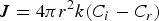
The physical and chemical properties of solvents and antisolvent solvents.
The processing window of antisolvents
The processing window of an antisolvent is defined as the time slot from the spreading of the perovskite precursor on the substrate to the treatment of the wet film with the antisolvent; this drip-wise washing with an antisolvent is required to obtain a dense with smooth coverage. Otherwise, treating the wet film outside the processing window would result in a rough and porous perovskite film, leading to short-circuiting of the final device. As nucleation occurs rather rapidly during antisolvent-assisted spin-coating, it can be difficult to control film morphology, resulting in a perovskite film with defects such as pinholes, inhomogeneous crystals, and grain boundaries. This means that an antisolvent must be dripped in a certain specific time period and in an appropriate volume ratio [96,97]. In a previous study [64], we found that DMF plays a key role in this process by extracting DMSO out of the wet film during antisolvent washing via the strong interaction between DMF and DMSO. There are two reasons for this narrow processing window of the antisolvent washing step, as follows. (1) DMF has a lower boiling point than DMSO and coordinates less strongly with Pb2+, and thus DMF evaporates faster than DMSO from perovskite precursor solutions containing a mixture of DMF/DMSO. This means that delaying the antisolvent washing time will result in much more DMSO than DMF remaining in the wet film before antisolvent washing, as illustrated in Figure 1(f). (2) The interaction between an antisolvent (such as CB or TL) and DMSO is too weak to extract DMSO out of a wet film, and therefore a substantial amount of unincorporated DMSO remains in a film even after antisolvent washing. This residual DMSO damages the perovskite film during thermal annealing, leading to films with poor morphology, i.e. having many pinholes and voids [98]. Thus, the use of antisolvents that interact strongly with DMSO or changing the precursor-solvent composition is effective strategies to widen the antisolvent processing window. It should be noted the principles discussed above with the representative spin-coating method could be more broadly applied to solution-based methods that are scalable.
Precursor-solvent engineering for widening the processing window
To make solution-based approaches compatible with large-area deposition technologies, it is necessary to widen the processing window, as this will enable the scalable fabrication of highly efficient solar cells. In recent years, extensive precursor-solvent engineering studies have been performed to widen antisolvent processing windows to permit effective control of the nucleation and crystal growth of perovskites, and thereby obtain films with uniform and pinhole-free morphologies [8,48,99–101]. Therefore, we comprehensively review the precursor-solvent engineering methods that have been reported for the solution-based fabrication of PSCs with wide processing windows, which involve control of the volume ratio of mixed solvents in precursors, solvent replacement, or the addition of diverse additives with specific functions to precursors.
Volume ratio of mixed solvents in the precursor
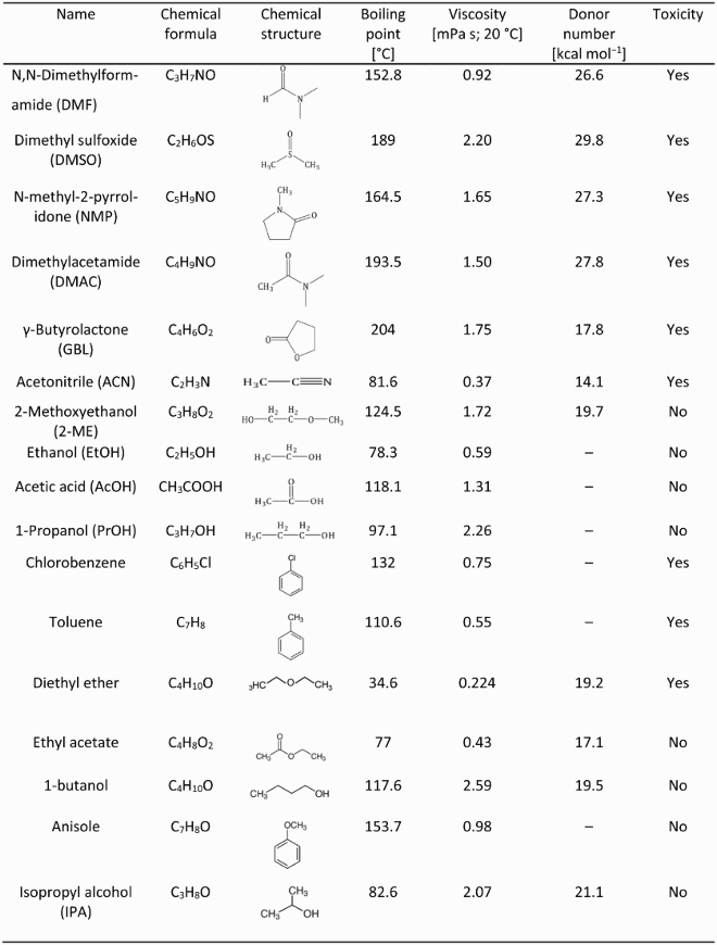
The precursor composition has an important influence on the drying window, which determines the width of the antisolvent processing window. It is influential because the antisolvent must be added to the wet film to wash out the excess solvent from the perovskite solute. Rong et al. reported an effective solvent engineering process to control perovskite crystal growth and widen an antisolvent processing window for the formation of perovskite films [102]. They achieved the latter by the addition of DMSO into a pure DMF solution. This resulted in the formation of intermediate complex phases that retarded the crystallization process and therefore provided more control of the final morphology of perovskite films. Zhu et al. widened an antisolvent processing window from 1 min to ∼8 min by tuning the composition of the solvent in the perovskite precursor solution [103]. Their precursor was an ink, which generated high-quality perovskite films with large-scale uniformity. They prepared various perovskite precursor solutions with different DMF/DMSO ratios (10:0 and 8:9 v:v) or a DMF/NMP mixture (8:9 v:v). These were spin- or blade-coated onto substrates, and the resulting coated substrates were washed in a diethyl ether (Et2O) bath for 30 s to complete the antisolvent solvent-extraction process. Subsequent removal of residual Et2O under nitrogen and annealing of the wet films at 150°C afforded the final perovskite films. They also investigated the effect of delay time on the blade-coating perovskite film-formation process by monitoring the average absorbance of films at 450–700 nm. It was found that the average absorbance of perovskite films made from pure DMF increased almost immediately after the coating step (Figure 2(a)), which indicates a rapid nucleation process and means that the antisolvent processing window of such films is narrow. This antisolvent processing window was widened by the use of mixed solvents: it was greater than 2 min with DMSO:DMF (9:8 v:v) but ∼8 min with NMP:DMF (9:8 v:v). The delay time also significantly influenced the PCE of the solar devices fabricated using various mixtures of solvents (Figure 2(b)). When DMF or DMSO/DMF was used as a solvent, the PCEs of the resulting devices decreased rapidly with increasing delay time. In contrast, when NMP/DMF was used as a solvent, the PCEs of the resulting devices were insensitive to delay times from 0.5 to 6 min, which is consistent with the time period before the optical properties of precursor films undergo a drastic change. (a) Average absorbance from 450 to 700 nm of perovskite films deposited by a blade-coating method using various solvents as a function of the processing delay time. (b) Effect of processing delay time on the PCE of PCS devices using the various solvents indicated in (a). Both images reprinted from [68] with permission. (c) Schematic diagrams of the antisolvent processing window for dissolving an MAPbI3·DMF complex in a low-volatility solvent (DMSO), and SEM images of MAPbI3 thin films prepared by antisolvent washing within the processing window. Reprinted from [8] with permission.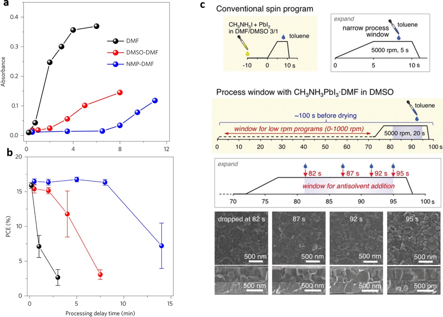
In addition, the evaporation rate of a solvent, which depends on its vapour pressure, also affects the width of the processing window. DMF has a high vapour pressure at room temperature (2.7 mmHg), which means that it evaporates rapidly during/after spin-coating; this accounts for the narrow processing window of perovskite films fabricated in a pure DMF solution. DMSO and NMP have much lower vapour pressures (0.42 and 0.29 mmHg, respectively) than DMF, which means that the introduction of DMSO or NMP into DMF can limit the evaporation of DMF during/after the coating process, thereby widening the processing window. Moreover, the viscosity of a solvent affects its evaporation rate, and thus also plays an important role in determining the width of the antisolvent processing window. Specifically, as the content of DMSO or NMP in a solution increases, the viscosity of the solution gradually increases, which slows the evaporation of solvent during perovskite fabrication. Thus, using DMSO rather than a DMF/DMSO mixture as a solvent can widen the drying window because of the higher volatility of DMSO, but the reduced solubility of perovskite solutes in DMSO means that it is typically more difficult to fabricate perovskite films of the required thickness from DMSO than from DMF/DMSO mixtures. To address this problem, Wakamiya et al. used a high-purity MAPbI3·DMF complex as a perovskite precursor and DMSO as a solvent (instead of DMF/DMSO mixed solvent) [8]. As this complex is highly soluble in DMSO, this led to a significantly wider drying window for the wet MAPbI3·film (13 s) in DMSO than that in a DMF/DMSO solvent (5 s), as depicted in Figure 2(c). They exploited this wider processing window to generate a device with a PCE of 14.2% and an active area of 22.0 cm2, thereby demonstrating the utility of this method for forming large-area spin-coated modular devices.
Precursor solution substitute
The interaction between a solvent and a solute also affects the crystallization process and the width of an antisolvent processing window. Hamill et al. found that the value of D N was strongly correlated with the ability of a solvent to solubilize a perovskite precursor: solvents with D N > 18 kcal/mol tended to solubilize precursors, whereas solvents with D N < 18 kcal/mol tended to accelerate the crystallization of precursors [75]. Thus, they observed that compared with a solvent with a low D N, a solvent with a high D N, such as N,N′-dimethylpropyleneurea (DMPU), complexed more strongly with Pb2+, thereby delaying the onset of perovskite crystallization. To exclude the possibility that this was due to the low vapour pressure (P vap) of DMPU (P vap = 0.039 mmHg), Hamill et al. spin-coated DMF-based perovskite solutions with propylene carbonate (PC; P vap = 0.023 mmHg) [75] as an additive, instead of DMPU. Although PC has a lower P vap than DMPU, PC coordinates less strongly to Pb2+ than DMPU. Thus, films spin-coated from precursor solutions containing PC additives did not exhibit delayed crystallization; instead, they turned black within 4 s after spin-coating. This confirmed that the delayed crystallization in the films cast from DMF/DMPU solutions was due to the strong interactions between DMPU and Pb2+. Hamill et al. also fabricated PSCs, incorporating a TL antisolvent washing step during spin-coating to extract residual solvent. They found that the incorporation of DMPU substantially widened the antisolvent processing window under these conditions.
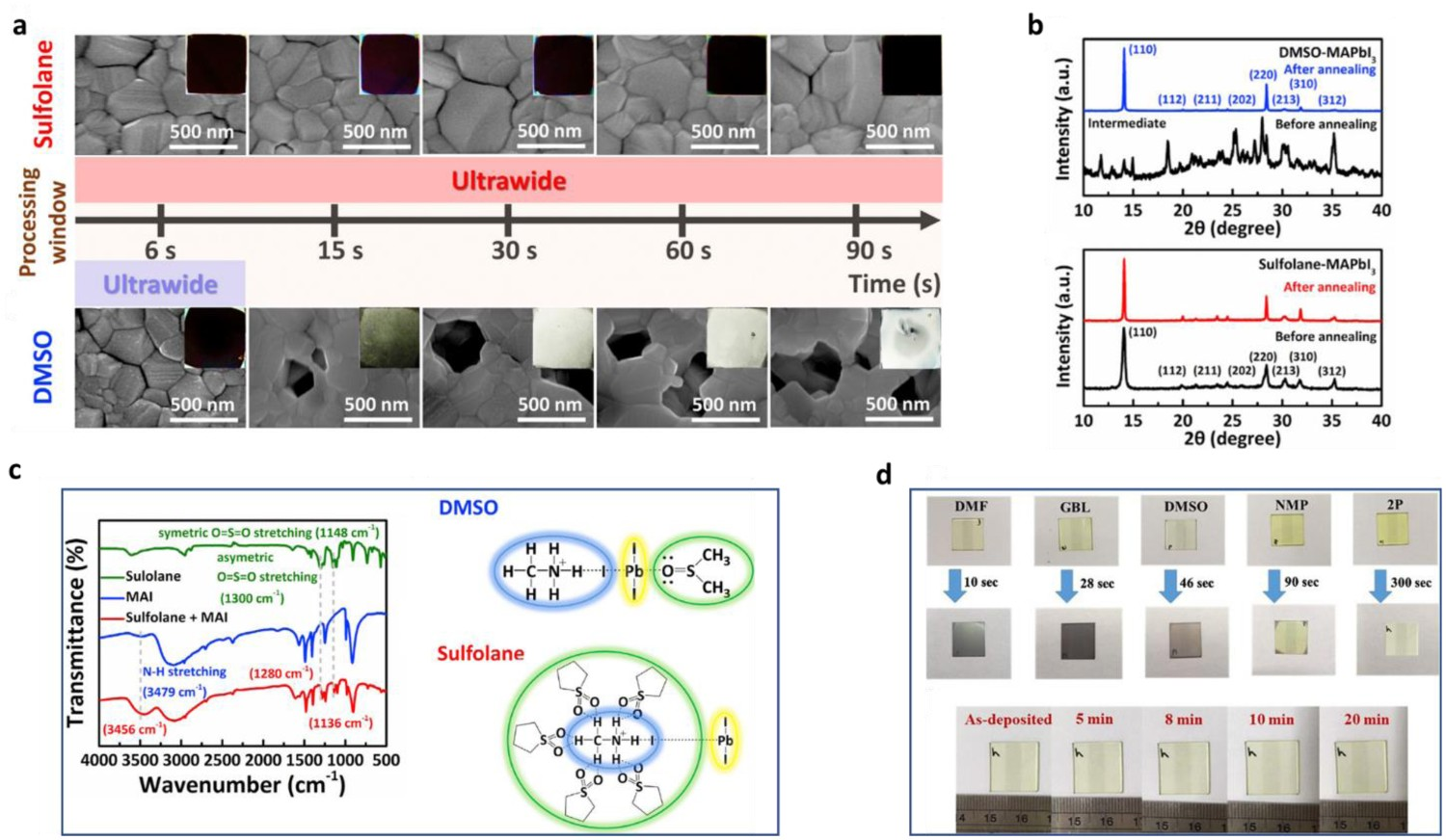
In addition, non-volatile solvents such as diphenyl sulfoxide (DPSO), sulfolane, and 2-pyrrolidinone (2P) have also been introduced into precursor solutions. Yang et al. reported the use of DPSO, a non-volatile (at room temperature) Lewis base additive with strong coordination ability [52], in FACs perovskite precursor solutions. DPSO retarded the natural nucleation of perovskite during a slot-die coating process and stabilized the wet precursor film, thereby widening the antisolvent processing window. They first investigated the morphological evolution of the wet films obtained from three solvent systems (DMF, precursor 1; DMF–NMP, precursor 2; and DMF–NMP–DPSO, precursor 3) by optical microscopy (Figure 3(a)). It can be seen that the stability of the wet films gradually improved when DMF was replaced with DMF–NMP and DMF–NMP–DPSO, which indicates that the uncontrollable nucleation and growth processes of precursor 1 were retarded by the introduction of NMP or NMP–DPSO into the system. Yang et al. also used FTIR spectroscopy to reveal the interaction between DPSO and other components within the perovskite precursor solutions [52]. As shown in Figure 3(b–d), the S=O bond stretching vibration peak was at 1037 cm−1 in DPSO but at 968 cm−1 in PbI2–DPSO, indicating the formation of a PbI2·DPSO adduct. Similarly, the stretching vibration peak of C=N was at 1715 cm−1 in FAI but at 1710 cm−1 in FAI–PbI2–DPSO, indicating the formation of an FAI·PbI2·DPSO product. These results confirmed that a much higher energy barrier must be overcome to enable perovskite nucleation/growth from a solution of DMF–NMP–DPSO than from a solution of DMF or DMF–NMP, and thus the strong coordination capability of DPSO led to a wider antisolvent processing window. Wang et al. introduced sulfolane as an additive into a perovskite precursor to convert the perovskite phase via a new reaction route [104], which provided a wide time window for the large-scale fabrication of perovskite layers with high uniformity (see scanning electron microscopy (SEM) images in Figure 4(a)). X-ray diffraction and FTIR results (Figure 4(b, c)) revealed that this was due to the intermolecular hydrogen-bonding between sulfolane and MAI (Figure 4(c)), which perturbs the physical interaction of MA+ and PbI3
− and thus slows the nucleation and crystallization process. Finally, they demonstrated a mini module with a 36.6-cm2 active area that exhibited a record-high PCE of 16.06% with an ultrawide processing window of up to 90 s. In similar work, Tseng et al. used the non-volatile and less toxic 2P as a complexing solvent in a perovskite precursor solution [100]. As shown in Figure 4(d), 2P stabilized the wet perovskite film for up to 20 min due to the formation of an MAI–PbI2–2P adduct, which led to a high-quality perovskite film. Such non-volatile solvents are useful for industrial-scale production conducted in the open atmosphere, as they decrease the risk of harm to workers. (a) Semi-in-situ optical microscope-based observation of the evolution of the perovskite precursor film morphology over time (scale bar, 100 µm). The perovskite precursors dissolved in DMF, DMF–NMP, and DMF–NMP–DPSO are denoted as precursors 1, 2, and 3, respectively. (b–d) FTIR spectra of fingerprint regions for C=O and S=O stretching vibrations. (b) C=O stretching detected in DMF (solution, black), PbI2·DMF (powder, red), FAI (powder, blue), and FAI·PbI2·DMF (powder, orange). (c) C=O stretching detected in NMP (solution, black), PbI2·NMP (powder, red), and FAI·PbI2·NMP (powder, orange). (d) S=O stretching measured for DPSO (powder, black), PbI2·DPSO (powder, red), and FAI·PbI2·DPSO (powder, orange). The blue lines represent the spectra of FAI (powder). All images reprinted from [52] with permission. (a) Top-view SEM images of a perovskite thin film (scale bar: 500 nm) prepared using various antisolvent dripping times and sulfolane or DMSO as a solvent. The insets are photographs of the final perovskite layer after conversion. (b) XRD patterns of the as-prepared and thermally annealed perovskite thin films prepared using DMSO or sulfolane. (c) FTIR spectra of sulfolane (solution), MAI (powder), and MAI/sulfolane mixture, and schematic illustration of perovskite formation via the MAI·PbI2·DMSO intermediate phase. The S=O moieties in sulfolane form hydrogen bonds with methylammonium ions (MA+), which perturbs the physical interaction of MA+ and PbI3
–. All images reprinted from [104] with permission. (d) Photographs showing the colour of precursor films prepared from precursor solutions using various solvents under an ambient atmosphere. Reprinted from [100] with permission.
Precursor additives
The antisolvent processing window can also be widened by introducing additives into a perovskite precursor. These additives tend to interact with precursor solute in solution, promoting the heterogeneous nucleation of the perovskite, which help to extend the perovskite processing window. In the process of fabricating MAPbBr3 film in dichloromethane, Zhang et al. incorporated trivalent neodymium ions (Nd3+) into perovskite thin precursor to control nucleation and crystal growth [105]. These pre-nucleated crystals in perovskite precursor make them less sensitive to rapid changes in the solvent environment during the high-speed rotation process, thus resulting in widening the processing window from 3–5 to 18 s (Figure 5(a)). They also noticed that the incorporation of Nd3+ improved the crystallinity of the resulting MAPbBr3 perovskite films. Similarly, Yang et al. demonstrated that the addition of a 15% excess of MACl into a perovskite solution tuning the nucleation and crystallization process and incorporated a fast-annealing process (∼1 min) could also greatly enlarge the thermal processing window (from 1 to 10 min) [103]. Furthermore, we recently found that 1,4,7,10,13,16-hexaoxacyclooctadecane (18-crown-6; 18C6) can be used as an additive in a triple-cation perovskite precursor [35] to significantly widen the antisolvent processing window to ∼20 s (Figure 5(b, c)) by stabilizing ternary perovskite precursor. The presence of 18C6 also significantly improved the reproducibility of device performance. We posited that the interaction between 18C6 and cations – especially Pb2+ and MA+ – at the surface of a perovskite crystal would inhibit its transition from the cubic 3C to the hexagonal 2H phase, which was verified by the grazing-incidence wide-angle X-ray scattering data we obtained (Figure 5(d)). Therefore, the high reproducibility of high-quality perovskite films was attributable to 18C6 effectively suppressing the generation of 2H phase perovskites. (a) Schematic diagrams of the process of preparing MAPbBr3 perovskite film via the antisolvent method and use of an Nd3+ additive, and schematic diagrams of the nucleation process and crystal growth. Reprinted from [105] with permission. (b) Schematic diagram of the deposition process of perovskite films without and with 18C6. (c) Optical photographs of C-poly(9-vinylcarbazole) (PVK) obtained with different processing times and CB volumes. (d) C-PVK annealed at 25°C, 105°C, and 225°C. All reprinted from [35] with permission. (e) Comparisons of the normalized PCEs of PSCs fabricated from thin films using anisole or CB and various processing parameters: DMF:DMSO ratio (6:4–9:1), antisolvent dripping time (5–25 s), and antisolvent dripping volume (0.1–0.9 mL). Reprinted from [98] with permission.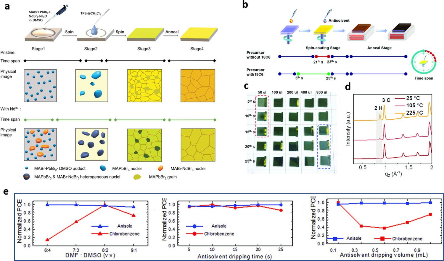
Perovskite composition control
The composition of a perovskite itself also affects the width of the antisolvent processing window, as it has been found that a perovskite with a single cation or a single halide anion has a narrow antisolvent dripping window [96,97]. For example, the width of the antisolvent processing window of an MAPbI3- or FAPbBr3-based perovskite precursor is only about a few seconds [106], whereas that of mixed halide anion- or mixed cation-based perovskite precursors ranges from tens of seconds to a few minutes [107]. This is possibly due to perovskite films containing a mixture of cations/halogens having a longer sol–gel (i.e. gelation) time during the formation of perovskite film than those containing a single cation [107].
Antisolvent engineering for widening processing windows
The technology of precursor engineering offers a new way to widen perovskite processing windows by retarding the evaporation of a solvent or by stabilizing a wet perovskite film. This assists with the generation of uniform and pinhole-free perovskites on large-area substrates, which is essential for accelerating the commercialization of PSCs. However, single PSCs with the highest PCEs are prepared from DMF/DMSO solutions with relatively fixed compositions, as a certain volume ratio of DMF and DMSO is required to effectively solubilize the perovskite solute and retard perovskite nucleation and growth during perovskite fabrication. Thus, antisolvent engineering has been explored as a means to widen perovskite processing windows and enhance the quality of perovskite films, thereby generating highly efficient PSCs with flexible processing times. Here, we review studies on this topic, which have included the use of new antisolvents and mixed antisolvents.
Novel antisolvents for wide processing windows
Antisolvent-assisted one-step solution deposition has been demonstrated to be the most effective strategy for fabricating dense and uniform perovskite films with low defect densities. The most commonly used antisolvents – CB, TL, and Et2O – have been widely used to fabricate high-performance PSCs that have PCEs exceeding 25.5%. However, these antisolvents typically have a narrow dripping time window, which can be easily missed, and thereby lead to devices with low performance. To solve this problem, Zhao et al. used anisole as an antisolvent, as this is a hydrogen-bonding acceptor [98] that forms hydrogen bonds (C─H⋅⋅⋅O) with hydrogen-bonding donors (C–H) in DMSO or DMF. Moreover, anisole–DMF–DMSO mixed solvents form a high-boiling azeotrope that facilitates the antisolvent-mediated solvent-extraction process. Specifically, the use of anisole as an antisolvent in a one-step spin-coating process enabled to fabricate perovskite thin films with an ultrawide antisolvent processing window of up to 25 s, where the DMF:DMSO ratio varied from 6:4 to 9:1 in the precursor solution (Figure 5(e)). They determined that there were two reasons for this wide processing window with the use of anisole as antisolvent. (1) Hydrogen-bonding between anisole and DMSO/DMF facilitated the extraction of residual DMSO (which had not formed an intermediate phase with PbI2) from the wet perovskite film. (2) The formation of a high-boiling anisole–DMF–DMSO azeotrope meant that the anisole–DMF–DMSO complex was resistant to volatilization during the spin-coating process, which protected the mixed state of intermediate and nucleating perovskite layers. More importantly, this antisolvent treatment facilitated the deposition of highly uniform large-area perovskite films without requiring the adjustment of any spin-coating parameters: thus, dense perovskite films with sizes of 4, 25, 49, 100, and 196 cm2 were fabricated.
We recently investigated the fundamental reasons for the narrow processing window of widely used antisolvents, and concluded that it has the following causes. (1) DMSO evaporates much slower than DMF due to its higher boiling point and much stronger interaction with PbI2 in a wet film than DMF, which means that a large amount of uncoordinated DMSO remains in a wet film before antisolvent washing. (2) The weaker interaction between widely used antisolvents (such as CB and TB) and DMSO, which means that they are less effective than other antisolvents at extracting residual DMSO out of a wet perovskite film. As this residual DMSO does not form an intermediate phase with PbI2 in the wet film, it can cause damage during annealing, leading to a final perovskite film with a non-uniform morphology filled with pin-holes [64]. We thus examined the performance of a series of non-toxic antisolvents – dimethyl carbonate, ethyl methyl carbonate (EMC), and diethyl carbonate (DEC) – as these interact strongly with DMSO. We performed density functional theory (DFT) calculations to understand the interaction between solvents and antisolvents. These calculations generated electron-density difference maps (as shown in Figure 6(a)) that illustrated that the greatest charge transfer – and thus the strongest interaction – occurred between EMC and DMSO, which was verified by the FTIR results (Figure 6(b,c)). This strong interaction between EMC and DMSO facilitated the removal of residual DMSO from the wet film within an ultrawide antisolvent processing window (∼35 s) (Figure 6(d)). Furthermore, we found that EMC, which is non-toxic, could be used to fabricate large-area flexible perovskite solar devices that achieved an average PCE of 16.78% on a 6 cm × 6 cm flexible poly(ethylene 2,6-naphthalate substrate. In a similar vein, Jung et al. applied (R)-(+)-limonene and 2-methyltetrahydrofuran as ‘green’ antisolvents for the fabrication of high-quality perovskite absorbers in inverted PSCs. The wide processing window of these antisolvents was demonstrated during the fabrication of both organic–inorganic and all-inorganic perovskite films. (a) Binding energies of dimer complexes based on DFT calculations. The blue (red) column denotes a complex in which the C−O (C=O) moiety of EMC is close to another molecule. Electron-density difference maps of EMC + DMF and EMC + DMSO dimer complexes are displayed. The green and blue regions represent electron accumulation and depletion, respectively; (b) and (c) FTIR at low and high wavenumbers for solvents and antisolvents; (d) optical photograph of perovskite films prepared using three antisolvents with various dripping times. All reprinted from [64] with permission.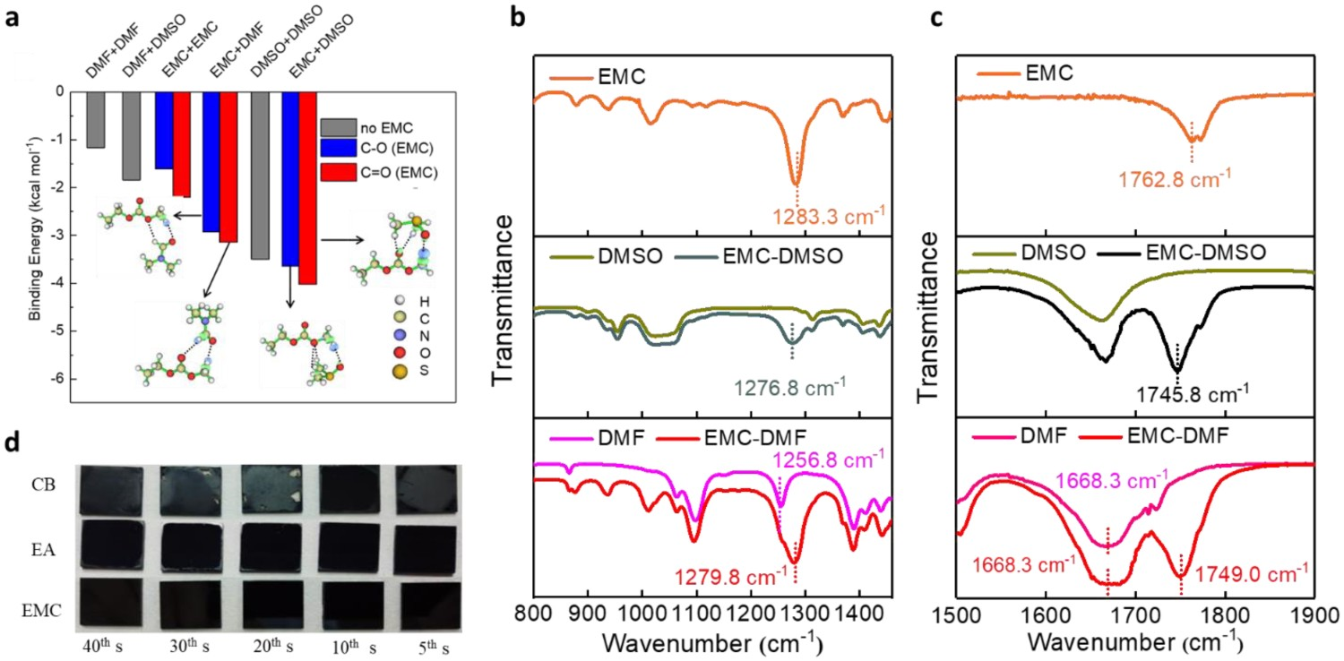
Mixed antisolvents for large processing windows
Inspired by mixed perovskite precursor engineering, mixed antisolvents have also been used to widen antisolvent processing windows. Kim et al. [99] used a mixture of tert-butyl alcohol (tBuOH) and ethyl acetate (EA) as an eco-friendly antisolvent in roll-to-roll (R2R) manufacturing of a FA-based perovskite (Figure 7(a)). The polarity of tBuOH is between that of straight-chain alkyl alcohols and esters, which means that tBuOH extracts DMF and residual DMSO without dispersing FAPbI3 or dissolving FAI in solution. This accounts for the homogeneous uniform FAPbI3 films that can be formed from tBuOH:EA. Kim et al. [99] also found that the strong interaction between tBuOH:EA and DMF and DMSO was responsible for the wide antisolvent bathing processing window (Figure 7(b)). Thus, by using TB:EA as a antisolvent, they fabricated full R2R gravure-printed flexible PSCs, aside from the top electrodes; the scalability of this process was demonstrated by the fabrication of 100-m-long rolls of solar panels with a high PCE (>16%). (a) Schematic diagram representing R2R processing of a perovskite layer. Details of each step of processing and timescales are presented. (b) Photographs of perovskite film after processing in various antisolvents. The images were captured from a video recording. Final films were obtained by thermal annealing of the intermediate film after processing in antisolvent for 20 s. All reprinted from [99] with permission.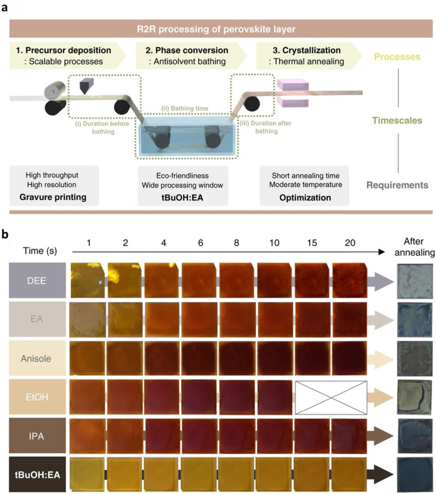
Inspired by the use of mixed antisolvents and based on our understanding of the reasons for narrow processing windows, we developed a universal approach for widening CB antisolvent processing windows based on antisolvent–solvent interactions [108]. This involved the addition of a small amount of three groups (I, II, and III) of small organic molecules (2–5% v:v) with a D
N value of 9.0��27.0 kcal mol−1 into CB to form a mixed antisolvent (Figure 8(a)). Pleasingly, these mixed antisolvents exhibited significantly widened processing windows (40 s, compared with 2 s without the additive) in precursor solutions containing DMF/DMSO in ratios that varied from 7:3 to 0:10. As shown in Figure 8(b), the perovskite films prepared using a mixture of CB and a group II (moderate D
N value) additive molecule had uniform and consistent mirror-black morphologies irrespective of the dripping time, whereas films prepared using an additive molecule from group I (low D
N value) or III (high D
N value) had non-uniform, rough, and gray morphologies. Similar trends are visible in the SEM images (Figure 8(c)). We concluded that an additive molecule with D
N = 9.0–27.0 kcal mol−1 had a moderately strong interaction with DMSO and thus extracted residual DMSO out of the wet film without damaging the perovskite intermediate phase, thus resulting in a wide antisolvent processing window. In contrast, an additive molecule with D
N < 9.0 kcal/mol had a weaker interaction with DMSO and thus could not extract residual DMSO, whereas an additive molecule with D
N > 27.0 kcal mol had a very strong interaction with Pb2+ and thus competed with I− and DMSO for coordination sites around Pb2+, which degraded the intermediate phase and led to a non-uniform film with poor morphology. These results were verified by FTIR spectroscopy. As shown in Figure 8(d), the S=O stretching vibration peak of DMSO was at approximately 1060 cm−1 but the addition of PC (D
N = 9.0–27.0 kcal/mol) caused it to shift to 1054 cm−1, indicating the strong interaction between DMSO and PC. In contrast, the FTIR peaks of DMSO–TB (TB: D
N < 9.0 kcal mol−1) systems showed no obvious shift, which indicates that the interaction between DMSO and TB is weaker than that between DMSO and PC. The distribution of device performance also varied due to the wide processing window that was created when certain mixed antisolvents were used to treat perovskite films (Figure 8(e)). This was attributable to these additive molecules facilitating the in-situ formation of perovskite crystal seeds, which served as a template for perovskite crystallization and thus decreased the intrinsic bulk defects in the resulting perovskite films. (a) Additive molecules used, classified into three groups (I, II, and III) based on their D
N values. (b) Optical photographs of the perovskite films prepared using various antisolvents and processed at various dripping times. (c) SEM images of the perovskite films prepared using various antisolvents/dripped at the 10th, 20th, and 30th second. All scale bars are 200 nm. (d) FTIR transmittance spectra of the pure solvents and perovskite solute/ions. (e) Average PCEs of devices formed using various antisolvents dripped at different times. All reprinted from [108] with permission.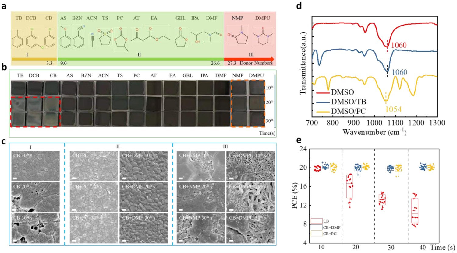
Strategies for widening processing windows for large-area device fabrication
To date, most high-efficiency single perovskite solar cell devices formed via antisolvent-assisted spin-coating technology have had small active areas (∼0.1 cm2). However, for commercialization, it is necessary to form highly efficient large-scale modules (>800 cm2). Various scalable coating techniques have been developed to produce large-area PSCs, such as doctor blading, slot-die coating, spray coating, screen printing, dip coating, and vacuum deposition. However, most of these methods produce perovskite films that are less smooth than those produced using antisolvent-based spin-coating technology. This is mainly because as the area of a film increases, its processing window becomes narrower due to the sensitivity and instability of the wet film, and also due to the variability of atmospheric conditions under which the fabrication is performed.
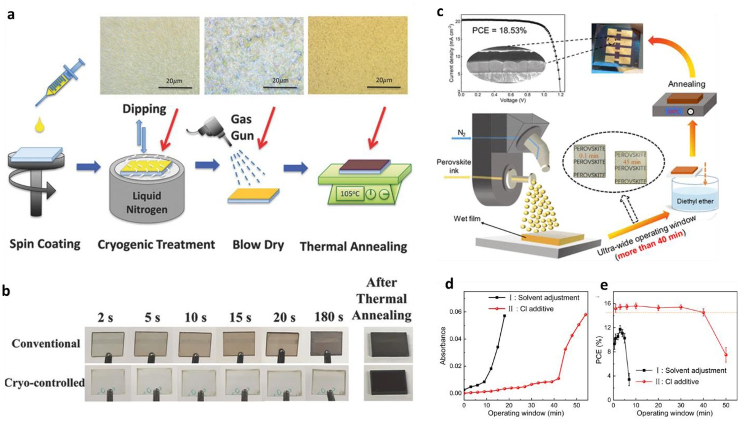
To widen the processing window of large-scale fabrication, Hu et al. reported a laminar air-knife-assisted room temperature approach for the controllable production of uniform and scalable perovskite films, and applied this approach to achieve hysteresis-free high-efficiency (20.26%, best PCE) PSCs with high reproducibility [109]. This antisolvent-free fabrication method exhibited a wide processing window (>12 min). Moreover, they investigated the perovskite film-formation process via in-situ ultraviolet–visible absorption spectroscopy and optical microscopy, which generated unique insights into the drying kinetics during the room-temperature meniscus-coating perovskite formation process. Figure 9(a) shows that the air-knife-assisted meniscus-coating process resulted in dramatically faster drying kinetics than those of the natural drying process. Therefore, the air-knife-assisted meniscus coating method resulted in a significantly accelerated evaporation of the solvent, and the fast-drying kinetics dramatically shortened the time required for the initial solution to exceed its saturation point. This led to a high degree of supersaturation, which could reach the maximum supersaturation limit due to the extremely high rate of solvent evaporation. Subsequently, a high density of perovskite nuclei was rapidly formed under nitrogen blowing (see the schematic inset (red circle) in Figure 9(b)), resulting in a very small cluster size and a uniform and smooth perovskite film. In contrast, under natural drying, there was a lower degree of supersaturation and a lower density of perovskite nuclei, which eventually grew to form large perovskite domains (green shaded area in Figure 9(c)) that had poor coverage. In another effort, Yang et al. [63] developed a material nucleation/growth competition theory for tuning the nucleation and grain growth of perovskite film, and then developed a new method—the gas-flow-induced gas pump method (GGPM)—for the fabrication of large-area highly efficient PSCs (Figure 9(d)). Use of the GGPM enabled a dense, uniform, and full coverage perovskite film to be easily fabricated within 5 s within a large pressure-parameter window (100 Pa to 1500 Pa), which facilitated continuous production by a simple operation. Thus, they formed 30 normal-planar PSC devices with an area of 1.1275 cm2 that achieved an average PCE of 15.63 ± 0.80%. Lemmer et al. reported a distributed feedback laser-based flexible digital inkjet-printing process to form MAPbI3 perovskite materials [57]. By increasing the content of GBL in the perovskite precursor, they were able to widen their vacuum-drying processing window for a flat perovskite surface to up to 480 s. Zhu et al. developed a solvent-vapour-assisted post-treatment to obtain a homogeneous perovskite intermediate phase after antisolvent extraction [110]. The homogenization of the intermediate phase facilitated the upward growth of perovskite film during their annealing process, leading to the formation of large grains with few horizontal grain boundaries. In addition, compared with non-solvent-vapour-assisted treatment, the solvent-vapour-assisted treatment widened the antisolvent processing window by 10 s (to 15–25 s). Surya et al. devised a cryogenic process to retard the crystallization of perovskite films, which eliminated the need for antisolvents and yielded high-quality perovskite films after thermal annealing [111]. This cryogenic process involved rapid cooling with liquid nitrogen, which decoupled the nucleation and crystallization phases by retarding chemical reactions in the wet perovskite films. Subsequently, the frozen film was blow-dried with nitrogen gas (Figure 10(a)), resulting in the uniform precipitation of seed layers due to the supersaturation of precursors at extremely low temperature. This also enhanced the rate of evaporation of residual solvents, which prevented the seed layers redissolving into the residual solvent. As a result, crystallization was very slow under cryogenic conditions and thus the processing window for film formation was much wider (up to 180 s, see in Figure 10(b)) than that under natural drying- or antisolvent-assisted extraction-based methods (a few seconds). Zhang et al. investigated the processing window of a single-pass spray-coating method using a perovskite ink (Figure 10(c)) [101], and adjusted the solvent component (DMF/NMP) of the perovskite ink to obtain an ultrawide processing window for spray-coating [101]. Moreover, they added MACl to the perovskite ink and applied an antisolvent soaking–extraction step, which resulted in the formation of a dense and smooth perovskite film with large-area uniformity. The sprayed PSCs, therefore, exhibited much better PCEs (18.5%) than those formed using previous methods, with a stable power output of more than 17% and a processing window that could exceed 40 min (Figure 10(d, e)). Zhang et al. also determined that the addition of MACl into the perovskite ink precursor not only inhibited the formation of δ-FAPbI3 but also promoted the reaction of PbI2 and the crystallization of perovskites in the preferred orientation, which greatly assisted the crystallization of large-grain-size perovskite films. (a) First derivative of the time-resolved absorbance at 500 nm for air-knife-blown and naturally dried samples. (b) The classical LaMer model explanation of the different nucleation and growth of the precursor solid films in three cases: with nitrogen blowing in the solution state (red line); with natural drying (black line); and with nitrogen blowing in the intermediate phase (blue line). (c) The nucleation and growth rates (black lines) as a function of the degree of supersaturation, and the corresponding grain-cluster size (purple line). The natural drying case with a low degree of supersaturation (cyan). All reprinted from [109] with permission. (d) Fabrication of the perovskite film via a gas-flow-induced gas pump method. Reprinted from [63] with permission. (a) The cryogenic process for nucleation and perovskite synthesis. The inset figures are images of the precursor and the perovskite films under an optical microscope. (b) The appearance of the type A precursor films prepared by the conventional method and the cryogenic process at various time-points after spin-coating. Both reprinted from [111] with permission. (c) Schematic illustration of a single-pass spray-coated perovskite film formed using a wet spray mode. (d) Average absorbance at 470–700 nm extracted from the absorption spectrum of wet films generated using various processing windows. (e) PCE of sprayed PSCs formed using different strategies and processing windows of various widths. All three images reprinted from [101] with permission.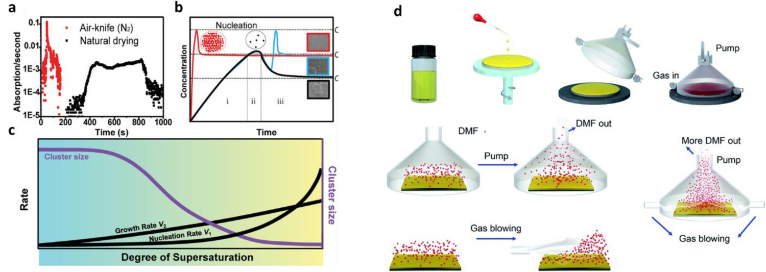
Another challenge to commercialization is posed by the strictly controlled environmental conditions that are required for device fabrication. For example, high-performance perovskite device production is usually performed in an inert or dry environment (relative humidity (RH) < 10%), and annealing processes should be controlled to run for only a specific time period. There is therefore an urgent need for new technologies or methods that enable perovskite fabrication to be performed under less rigorous and more flexible environmental conditions. Here, we review recent studies in this area. A first example is some of our recent work, in which we used previous results to develop a new air-knife-assisted recrystallization method to fabricate high-quality perovskite films in open air with wide RH control [112]. As shown in Figure 11(a), a PbI2–DMSO complex in DMF solution (PbI2(DMSO)/DMF) was coated onto a substrate in air, forming a well-covered wet PbI2 film containing a certain amount of moisture. We observed that an appropriate amount of moisture promoted the formation of nucleation sites, which facilitated the penetration of the MAI solution in the subsequent bath-immersion process. Then, we used air-knife processing to load the precursors into (or retain them within) the gaps between the perovskite cuboids. A subsequent annealing process resulted in the formation of residue-free and smooth perovskite films. To study the effect of DMSO and moisture on PbI2 film morphology, we fabricated PbI2 films in a glove box (GB) filled with inert gases, in a 25 ± 5% RH (25 RH) air environment, and in a 50 ± 10% RH (50 RH) air environment, respectively. As shown in the insert of Figure 11(b), all the PbI2(DMSO)/DMF films were semi-transparent, despite their formation under different RHs (from GB to 50 RH), suggesting they had high moisture-stability. Here RH processing window refers to the ambient humidity range in which dense perovskite film could be obtained when the fabricating process is performed in an open air. Finally, we demonstrated that a wide RH processing window (20–60% RH) Figure 11(c)) led to devices with very similar PCEs (19.28–19.39%). (a) Schematic representation of the method designed for preparing perovskite films. (b) SEM cross-sectional views of PbI2 films fabricated using PbI2/DMF and PbI2(DMSO)/DMF precursor solutions under the following conditions: I and IV – inert-gas glove box (GB; both compact films); II and V – 25% ± 5% RH; III and VI – 50% ± 10% RH; scale bar: 200 nm; insets are photographs of the real PbI2 films. (c) Real images of GB, 25%RH, and 50%RH PbI2(DMSO)/DMF films processed for various bath-immersion times, demonstrating their RH-dependent morphologies and porous structure-enhanced conversion. All reprinted from [112] with permission.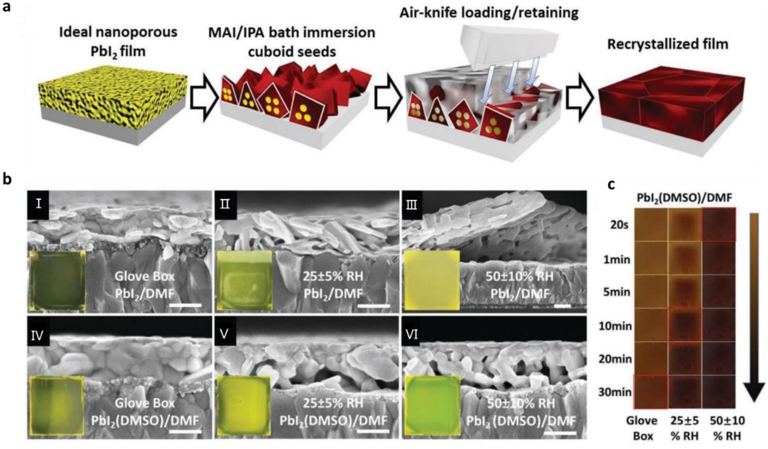
In solution-based processing approaches, DMSO has been widely used as a high-viscosity additive for perovskite precursors, as it strongly coordinates with PbI2 and is thus used to adjust crystallization dynamics. For example, Tian et al. [113] used DMSO and an additional heating reaction to create a hot air-flow process for forming all-inorganic perovskites (Figure 12(a)). They used this process to form devices from a wide range of solvent components; these devices exhibited a remarkable open-circuit voltage of 1.315 V and had a wide processing window (Figure 12(b)). In addition, the entire process could be conducted in ambient air with an RH of 15–25% and the resulting devices exhibited no loss of performance, which is ideal for the fabrication of large-area devices. (a) The hot air-flow (HAF)-assisted process and optical images of the initial wet film, the processed film after HAF processing, and the annealed film. (b) Vapour pressure of mixed solvent and solubility of CsPbI2Br (CPI2) as a function of DMSO content. Schematic representation of the method designed for preparing perovskite films. Both reprinted from [113] with permission.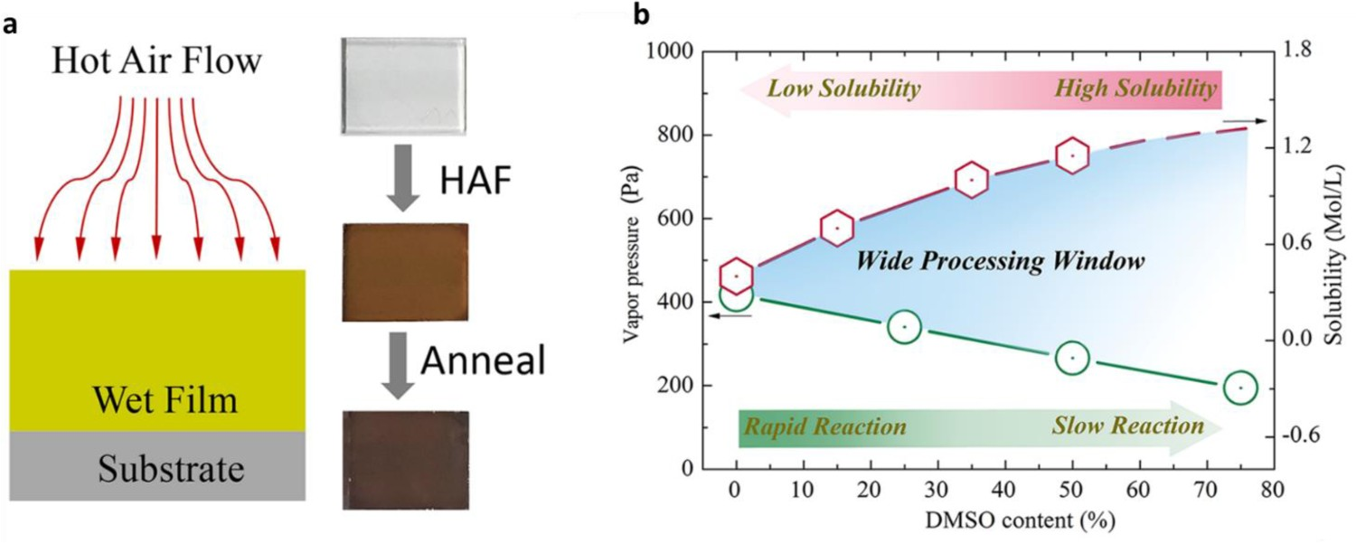
As the presence of Pb in perovskites may result in their damaging human health, Pb-free perovskite-based solar cells have also been widely investigated in recent years. In this regard, tin (Sn) perovskite-based solar cells have become the most promising candidates. However, the poor crystallization and chemical stability of Sn-based perovskites are two key problems; in addition, their processing windows must be improved to facilitate the development of Sn perovskite-based solar panels. Recently, Han et al. reported a strategy to stabilize an FASnI3-based perovskite with an amine complex, CH3NH3I·3CH3NH2, which profoundly inhibits perovskite degradation caused by the oxidation of Sn2+ to Sn4+ [114]. Compared with perovskite films formed from FASnI3-based perovskites without CH3NH3I·3CH3NH2, those formed from FASnI3-based perovskites containing CH3NH3I·3CH3NH2 displayed better crystallization and stability due to their processing window being up to 180 min wide. In addition to suppressing the oxidation of Sn2+ from the aspect of solvent coordination, Han et al. also introduced a carbonylate antioxidant capping layer atop the perovskite surface to prevent oxygen permeation into the perovskite film during the perovskite fabrication process [115], which enlarge the oxygen region from 0.1 to 100 ppm.
Conclusion and future prospects
This systematic review summarizes state-of-the-art developments in solvent/antisolvent engineering that widen the processing window of perovskite films for the fabrication of PSCs. Solvents and antisolvents play a significant role in solution-processed PSCs, because both greatly affect the crystallization of perovskite films. Moreover, the narrow processing window of perovskite films limits their commercial-scale application to form PSCs. We focus our review on studies that have examined three key aspects: (1) the role of solvents and antisolvents; (2) the use of solvent and antisolvent engineering to widen the antisolvent processing window of perovskite film fabrication; and (3) strategies for widening the processing window of large-area Pb PSCs and Pb-free PSCs. We hope that this review serves to illustrate the importance of considering the factors and mechanisms determining the width of perovskite film-processing windows, and the methods that can be used to widen processing windows to enhance the quality of perovskite film products (Figure 13). Summary of the key points of this review. Top left and bottom right figures reprinted from [61] with permission.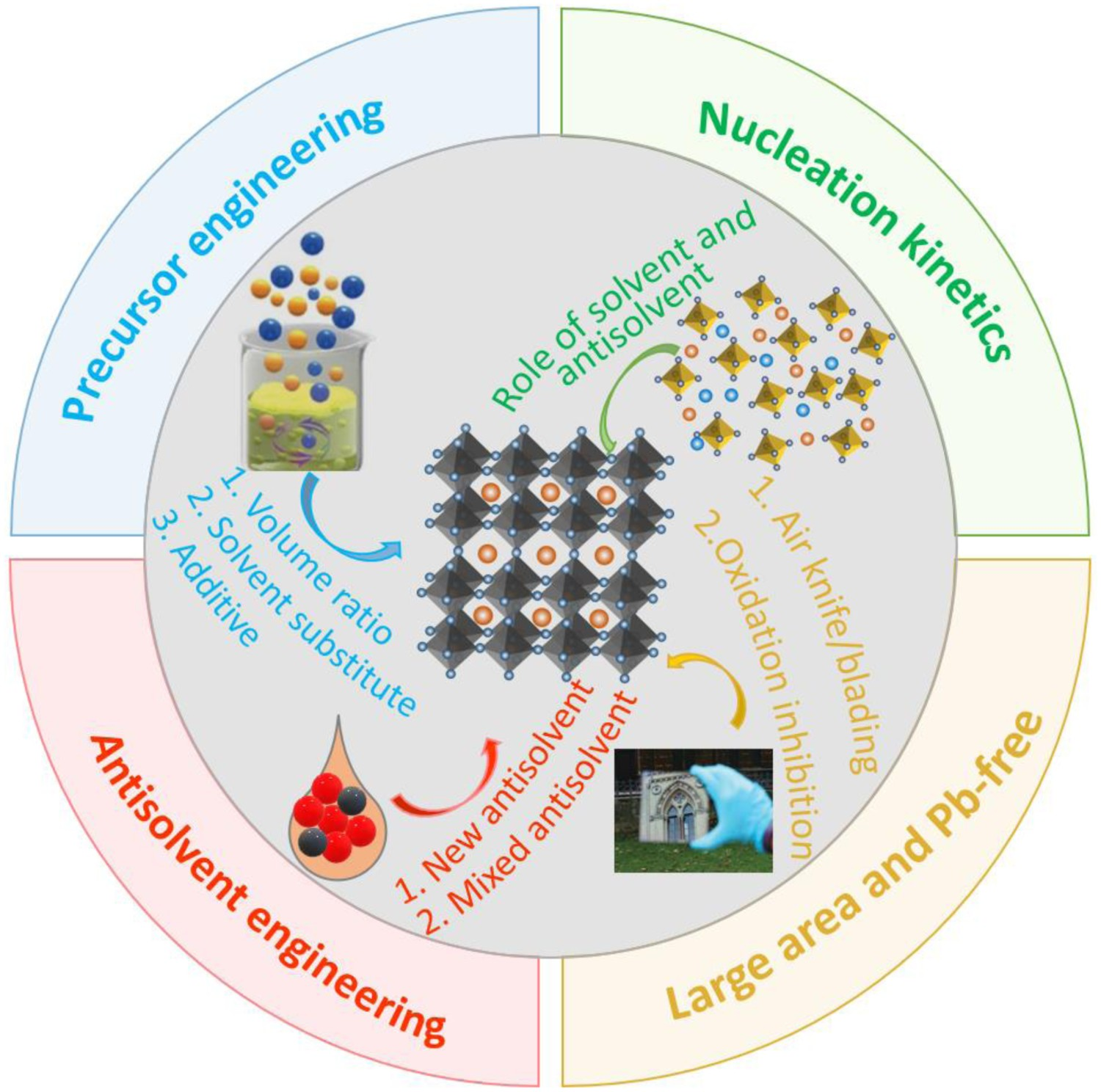
The narrow processing window of perovskite films is largely due to the sensitivity and changeability of these films when they are in a wet state. This is because solvents rapidly escape from wet films, which results in rapid and random nucleation and thus perovskite films with rough morphologies. Precursor solution engineering studies have shown that the rate of solvent evaporation is significantly affected by a solvent’s boiling point, vapour pressure, viscosity, and strength of coordination with Pb2+. Thus, a solvent with a low evaporation rate tends to have a wide processing window. To date, polar solvents with high boiling points and low evaporation rates, such as DMSO, NMP, DMPU, and sulfolane, have been used as additives in perovskite precursors. These additives strongly interact with the perovskite solute, forming a complex that stabilizes the wet perovskite film intermediate; this retards perovskite nucleation and crystal growth, which leads to a wide perovskite film-processing window.
Antisolvent engineering studies have explored the utility of new antisolvents, such as EMC, DMC, DEC, EA, and anisole, and mixed antisolvents, such as EA:tBOH and CB:DMF, to widen antisolvent processing windows. These antisolvents or additives tend to strongly interact with DMSO (via hydrogen-bonding), which helps to extract residual (and thus uncoordinated) DMSO out of wet films. This creates a wide antisolvent processing window and improves the quality of the perovskite films. Large-area antisolvent-free devices have been fabricated using a range of approaches; these have included the use of blown hot air or N2, or cryogenic processing, to stabilize the sensitive wet film state and thereby widen the processing window.
Although much progress has been made, particularly in solvent/antisolvent engineering, great challenges remain in this area. For example, insights into the fundamentals of the interaction between solvents and perovskite solutes or antisolvents are needed to provide a theoretical basis for solving the current and future problems in other large-scale manufacturing approaches to form perovskite films, such as blade-coating, spray coating, slot-die coating, and inkjet printing. To further meet the demand for near-future commercialization of PSCs, solvent/antisolvent engineering is undoubtedly a key factor to achieve a wide processing window, as this will enable the generation of highly efficient and reproducible PSC modules. Therefore, the following aspects should be considered for the further development of PSCs. More attention must be paid to the instantaneous dynamic changes of solutes, solvents, and antisolvents at the atomic or molecular level. This will help to reveal the mechanism underpinning various factors’ influences on crystallization and processing window widths. Although some models have been devised to illustrate the crystallization process, there is no accurate model that describes the formation of all types of perovskite films, especially those that are formed using antisolvents. There is a need for non-toxic and stable solvents with low evaporation rates. To accelerate the large-scale commercialization of PSC modules, environmental pollution and operator safety must be properly considered. Although some methods have been developed that use less toxic solvents, the most popular solvents for the fabrication of high-efficiency PSCs remain toxic organic solvents such as DMF. Moreover, solvents must have low evaporation rates, as this is important for wide processing window fabrication and ensuring the solubility of perovskite solutes. There is a need for a universal approach for the fabrication of Pb-free perovskite-based devices with wide processing windows. Thus far, few researchers have examined how to widen the narrow processing window in the fabrication of Pb-free PSCs. In the case of tin perovskite, the narrow processing window is mainly attributed to the fast reaction rate between the tin halides and organic salts due to the stronger Lewis acidity of Sn2+ than that of Pb2+, as well as the Sn2+ oxidation. Therefore, further additive engineering in precursor solution to reduce the reaction rate and suppress the undesirable oxidation process simultaneously should be done in the future.
Footnotes
Disclosure statement
No potential conflict of interest was reported by the author(s).
ACKNOWLEDGMENT
The authors acknowledge the support received from the Guangdong Provincial Engineering Technology Research Center for Transparent Conductive Materials.