
Abstract
A comparative investigation on the wettability and tensile strength of a Sn–2Ag, a Sn–40Bi and the traditional eutectic Sn–Pb solder alloys was carried out. The wettability is represented by thickness of covered layer (TCL) and spread area (SA) while the mechanical behaviour by the ultimate tensile strength (UTS). It is shown that the TCL of studied alloys decreased with the increase in the dipping temperature. It is also shown that TCL and SA have opposite behaviour with respect to the cooling rate. The Sn–Bi solder alloy has lower SA when compared with those of the Sn–Ag solder when similar cooling rates are considered. The Sn–Bi solder exhibits the best UTS/SA combination for dendritic spacings between 25 and 27 µm, associated with cooling rates ∼2°C s−1, 2× lower than those of the Sn–Ag alloy. Besides, the Sn–Bi alloy has shown SA >70∼80% associated with higher UTS (∼80 MPa) as compared with the other alloys examined.
Introduction
During 30 years, the Sn–Pb solders have been widely used due to their wetting performance and low cost associated with effective solderability in a number of industrial applications: water piping, food and beverage cans, automobile bodies and interconnection.1-10
Considering the toxicity of both Pb and Pb-containing materials and their negative effect to the environment, a variety of Pb-free solders have been proposed as successors to the traditional Sn–Pb alloy: Sn–Cu, Sn–Ag, Sn–Bi and Sn–Zn, as well as certain ternary and quaternary alloys.8-15 Additionally, directives from the European RoHS and the US Environmental Protection Agency8-10 imposed restrictions to lead application.
It is known that thermal stresses and strains during operation and/or heating in reflow treatments induce damages/distortions to soldering joints of electronic devices.16-17 The development of innovative materials, for sensitive to moderate temperatures, pushed investigative efforts towards the design of affordable solders with suitable melting temperatures. 18 Both wetting and mechanical behaviour are also very important parameters associated with the aforementioned requirements. In this sense, it would be very helpful to have tools permitting the control of the soldering process with a view to permitting the mechanical performance of the solder joint to be improved. It is well known that thermal-processing variables can be used in the control of solders microstructures. This permits appropriated unsoundness, strength, ductility and corrosion/oxidation behaviour to be achieved.7-9, 18, 19 Studies dealing with the interrelation wetting/tensile strength/microstructure of lead-free solder alloys are scarce. In this investigation the novelty is constituted by a correlation wettability/tensile properties as a function of microstructural features, at typical working soldering temperatures (e.g. 230–300°C).
Although the wettability of solders on different substrates can be widely characterised by a number of techniques, the thickness of the covered layer (TCL) on a substrate has also an important role on the joining performance. The dependence of TCL on the dipping temperature (T) and cooling rate (dT/dt) during flow/reflow and their corresponding microstructures, which considerably affects the tensile strength, has been demonstrated in a previous study. 16 It was reported that the TCL of the eutectic Sn–Pb solder on a Cu substrate decreased with increasing T. It was also found that three distinct Sn–Zn solders have evidenced slight increase in TCL with the increase in T. 16 Both the Sn–40 wt-% Pb and the Sn–Zn solders revealed quite similar TCL between 230 and 250°C. Besides, the Sn–9 wt-% Zn alloy attained an ultimate tensile strength (UTS) of about 60 MPa and elongation of about 30%. 16 Comparative studies among different solder alloys permitting the establishment of wetting-to-strength combination as a function of T and microstructure features can be important to broaden the spectrum of solders applications. For example, although the control of the cooling rate in an industrial flow/reflow is not an easy task, considering a determined solder alloy and the corresponding contact pads from a determined electronic circuit, this important parameter (i.e. the cooling rate) can be monitored using specific thermocouples (J-type with 0.25 mm diameter) at strategic locations in the reflow oven. Although a number of distinct circuits are applied in various soldering techniques (e.g. Surface-mount technology (SMT), Through-hole technology (THT) or mixture), when both the solder alloy and the circuit board families are adjusted (e.g. when a Printed Circuit Board (PCB) has predominantly SMT components), the temperature and time of soldering (reflow) can be pre-experimented in order to provide a more adequate cooling rate based on desired microstructure features and corresponding properties.
The aim of this paper is to develop a comparative experimental study of the main features of two distinct solder alloys; Sn–2 wt-% Ag and Sn–40 wt-% Bi; using features of the eutectic Sn–40 wt-% Pb alloy as references. Both Sn–Ag and Sn–Bi alloys are lighter (up to ∼20%) than the Sn–Pb alloy, however, the former one is considerably more expensive (up to ∼three times) and the latter has a compatible relative cost with a number of alternative solders. This study aims to examine experimentally: wettability behaviour (spread area (SA) and TCL), tensile behaviour and microstructural features, and to establish interrelations of these parameters with a view to contributing to the pre-programming of appropriate final properties of solder joints.
Experimental Procedure
Materials
Commercially pure Sn (99.991 wt-%), Ag (99.993 wt-%), Bi (99.992 wt-%) and Pb (99.83 wt-%) were used to prepare the three solder alloys (i.e. Sn–2 wt-%Ag and Sn–40 wt-%Bi) and the traditional Sn–40 wt-%Pb alloy. The alloys were prepared using alloying elements in a fixed proportion, which were melted in a refractory crucible in a muffle furnace heated by Kanthal-A1 heating elements, under argon atmosphere. Sn was melted first and then elemental solute pieces were added to the melt. Both alloy components were mixed well and allowed to remelt further for three times to guarantee homogenisation.
Dipping
In order to determine the SA and their corresponding TCL for each alloy, Cu plates of 150 mm × 20 mm × 1.5 mm, degreased in NaOH and HCl solutions, were used as substrates. The dipping procedures were carried out at dipping rates of 12–15 mm s−1, similar to those reported in previous investigations.1, 16 Different T were used (i.e. 300°C, 250°C, 230°C and 210°C ± 2°C) in air atmosphere. The Cu plates were dipped into the distinct molten alloys during about 3 s, corresponding to dipping depths of 70 mm for the Sn–Pb alloy and of 100 mm for the Sn–Ag and Sn–Bi alloys. 16 Two distinct dipping depths were experimentally tested. However, it was verified that these depths provide similar thermal and microstructural conditions. For this reason, the depth was parameterised for any experiment carried out. The experimental set-up used has been detailed in a previous study. 16 The optical microphotographs of each alloy examined were analysed by the ImageJ® software in order to determine both SA and TCL on the Cu substrate (transverse section). An image processing system was used to analyse the scale of the microstructural array (secondary dendrite arm spacing; λ2), SA and TCL. In order to determine λ2, at least, 10 measurements were considered for 3 distinct selected positions.
Microstructure and tensile testing
An etching solution of 92% (vol.) CH3OH, 5% (vol.) HNO3 and 3% (vol.) HCl for 5 s was used to reveal the microstructures. Specimens of the different alloys with similar microstructures, that is, related to similar dT/dt attained in the dipping stage, were used to determine UTS. The tensile tests were carried out according to the ASTM Standard E 8M/04. Triplicate tests were conducted in order to ensure reproducibility. The specimens were withdrawn from particular regions along the casting associated with particular dT/dt, as detailed in a previous study. 16
The schematic representation of the dipping technique is shown in Fig. 1
a. In order to measure the temperature of the molten solder and the Cu substrate thermocouples (type J) were used and dT/dt for each alloy was determined from the cooling curves. Figure 1
b depicts a typical covered sample after dipping and its corresponding section is schematically represented in Fig. 1
c. The typical microstructure of each alloy was characterised (Fig. 1
d) in order to permit the appropriate correlation with the specimen for tensile tests (Fig. 1
e). It is worth noting that the tensile tests were carried out in specimens produced by directional solidification under a wide range of dT/dt, thus permitting to associate particular tensile strength results with the samples obtained for similar dT/dt during dipping.
Schematic representation of: a dipping, b SA of solder samples, c cross section of covered plate, d typical microstructure array correlated with dT/dt and e tensile testing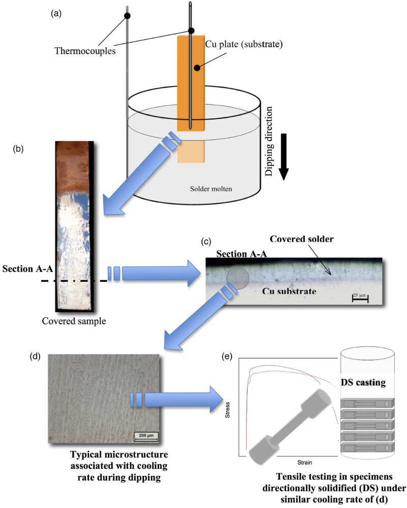
Results and discussion
Dipping tests: SA and TCL
Four distinct T (300°, 250°C, 230°C and 210°C) were selected to simulate soldering operation. Typical photographs of the as-dipped Sn–Ag, Sn–Bi and Sn–Pb alloys on Cu substrates for different temperatures are shown in Fig. 2.
Typical photographs of as-dipped Sn–Ag, Sn–Bi and Sn–Pb solder alloys on Cu substrates at distinct T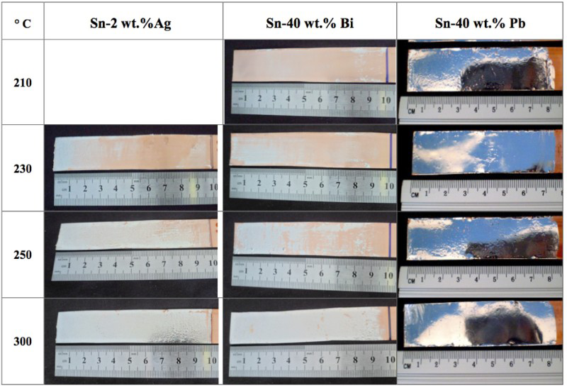
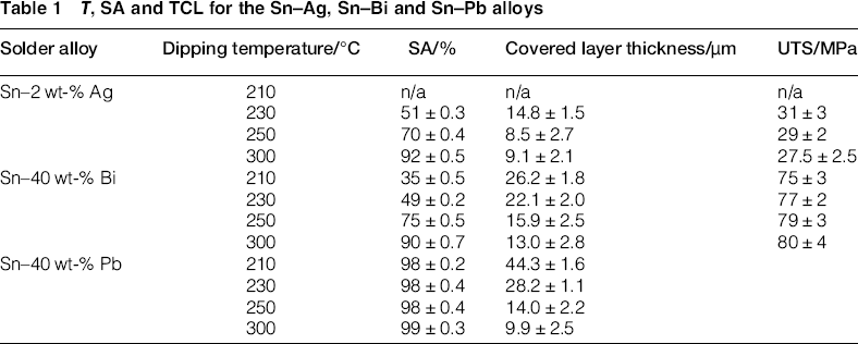
T, SA and TCL for the Sn–Ag, Sn–Bi and Sn–Pb alloys
Both the poor adhesion and SA of a solder alloy on the substrate are intimately affected by low viscosity. It is interesting to observe that both Sn–Ag and Sn–Bi solders have poor adhesion (<70%) at T < 250°C. At 300°C, the experimental measured SA is >90% for both alloys examined, which satisfies the requirement of soldering temperature practice. A previous investigation on Sn–Zn alloys reported that these alloys present lower SA when compared with that of the traditional Sn–40 wt-% Pb alloy at T = 300°C. 16 This corresponds to an inverse trend when compared with the results of the present investigation concerning SA versus T, that is, the Sn–Zn alloys have SA decreased with the increase in T.
Figure 3 depicts the experimental cooling curves acquired during dipping of Sn–Ag and Sn–Bi alloys recorded after 3 s of dipping at 300, 250, 230 and 210°C. dT/dt was determined for all temperatures, and an average dT/dt of about 8–10°C s−1 was established for both Sn–Ag and Sn–Bi alloys before the eutectic reactions, that is, 210 and 126°C, respectively. The eutectic and liquidus temperatures can be obtained from the corresponding phase diagrams.
8
The cooling curves for any alloy examined indicated average dT/dt of 5–6°C s−1. The experimental dT/dt during dipping of the Sn–40 wt-% Pb alloy has been previously reported to be about 10°C s−1.
16
Cooling curves obtained in the dipping tests for: a Sn–2 wt-% Ag and b Sn–40 wt-% Bi solder alloys after 3 s of dipping at distinct temperatures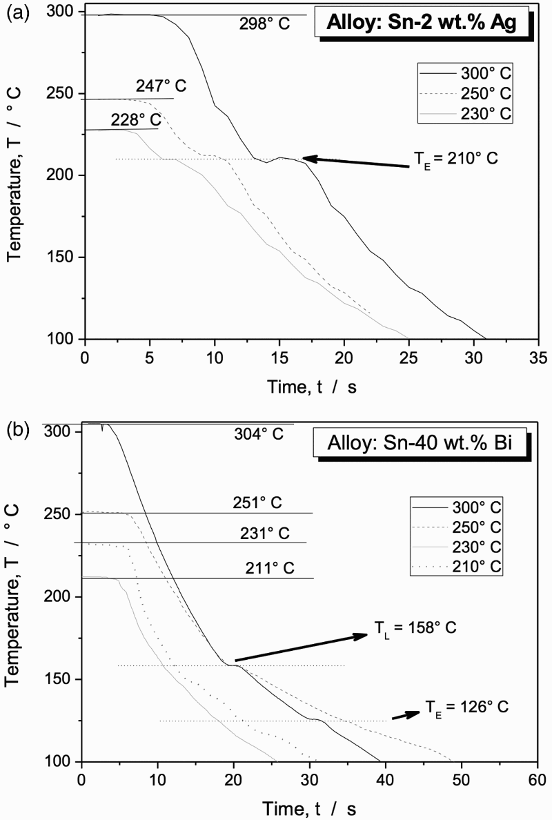
The resulting TCL of each alloy examined after dipping tests at 300, 250, 230 and 210°C are shown in Fig. 4. Based on these cross sections microphotographs, TCL as a function of T was determined (Table 1).
a Typical microphotographs of the cross sections, and thicknesses at b 230°C, c 250°C and d 300°C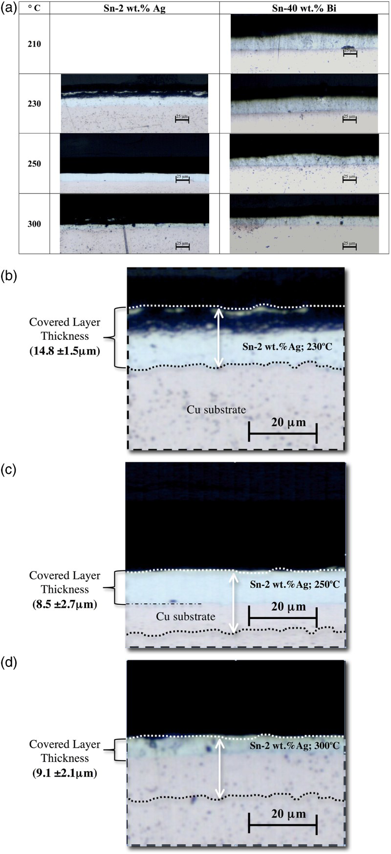
Another interesting observation is that any alloy examined tends to have TCL decreasing with the increase in T (Fig. 5
a). Previous investigations reported a slight increase in TCL with increasing T for three different Sn–Zn solders.16, 20,
21
TCL and SA percentage as a function of: T a and b, dT/dt c and d, and λ2 e and f for the alloys examined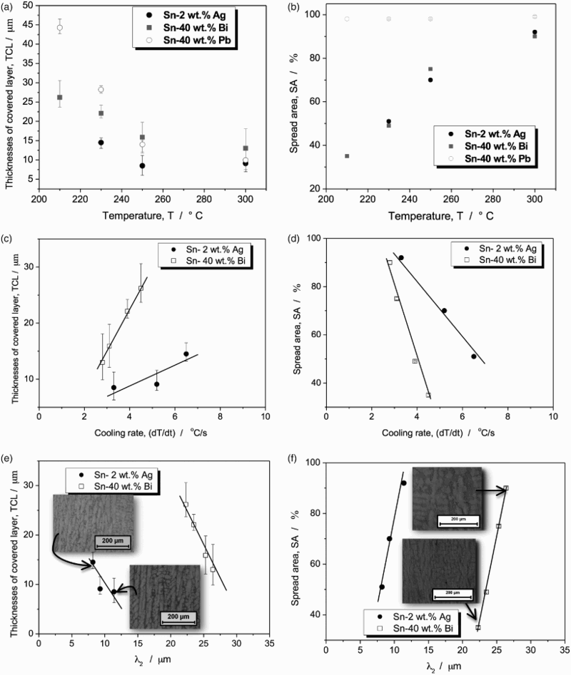
Figure 5 b shows SA versus T for Sn–Ag and Sn–Bi alloys compared with that of the Sn–Pb alloy. It is clearly observed a growth trend of SA for both Sn–Ag and Sn–Bi alloys, while for the Sn–Pb alloy no significant variation with T exists. Besides, it can also be seen that SA = f(T) has an inverse behaviour when compared with that of TCL = f(T). Because higher wettability is commonly provided by higher T, the growth of thicker layers is expected, as shown in Fig. 5 a.
It is well known that the solidified thickness is dependent on the solder/substrate heat transfer coefficient (h). The growth of thicker layers will be favoured by higher T, and the increase in h is associated with increase in the wettability. As the dipping experiments were carried out vertically, it is expected that a better adhesion between molten solder alloy/substrate exists, which in turn will assure an increase in wettability with increasing T. It is worth noting that h has an abrupt variation at the onset of dipping or solidification, when h is the highest and typically expressed by h = Ct−n, where C and n are constants and t is time. With the solidification evolution, h experiences a gradual decrease. 22 This coefficient is intimately associated with thermophysical properties of the materials (e.g. viscosity, surface tension, solute content etc.).22, 23
Considering non-equilibrium solidification of a Sn–2 wt-% Ag alloy, the primary solid is a dilute solid solution of Ag in Sn (of about 0.028 wt-% Ag) having a dendritic morphology with a eutectic mixture in the interdendritic region. A cooperative growth of Ag3Sn intermetallics (∼ 73 wt-% Ag) and the Sn-rich phase (of about 0.05 wt-%Ag) forms the eutectic. On the other hand, the examined Sn–40 wt-% Bi alloy has the primary solid with about 15 wt-% Bi considering an equilibrium partition coefficient of 0.368. Under high dT/dt, hypoeutectic Sn–Ag alloys have a Sn-matrix of dendritic morphology and Ag3Sn (spheroid-like particles) homogeneously distributed into the Sn dendritic matrix. It is well known that without intermetallics (IMC), the solder/substrate joint is weak due to the absence of appropriate bonding, which provides a deleterious effect in terms of electronic packaging. 24
It is very important to distinguish the IMC layer formation at the interface Sn-based alloys/Cu substrate and the Ag3Sn IMC's. The former IMC is commonly lower than 5 µm or at nanoscale and a scallop-type Cu6Sn5 IMC is formed. The latter IMC is formed by a cooperative eutectic growth, as previously mentioned. For reflow under a quite long period, the Cu6Sn5 IMC layer can grow significantly. A thick IMC layer at the solder/Cu substrate interface degrades the reliability of the solder joint. 24 The Cu6Sn5 layer forms when Cu is instantaneously absorbed by the molten solder, providing metallurgical bonding.
Owing to Cu saturation adjacent to the molten solder, the Cu6Sn5 IMC grows depending on of the local thermodynamics condition. 1 The growth mechanisms of the IMC layer have been reported.24, 25 Lee and Mohamad 24 reported the typical growth mechanisms of Cu6Sn5 at Sn–Ag–Cu/Cu interfaces, as well as the evolution of the IMC thickness with time and temperature. Su et al. 25 studied the typical morphology of IMCs formed at the Ag/Sn interface and in the Sn matrix after soldering at distinct temperatures and times. Zhao et al. 26 have also shown how an IMC-coated Cu substrate affects the wetting behaviour of lead-free solders. Besides, there are a number of other articles considering the IMC layer,27-29 which has motivated the aim of this present investigation to be mainly focused on the interrelation wettability/microstructural features/tensile strength considering the bulk of both Sn–Ag and Sn–Bi alloys.
Lee and Mohamad 24 reported growth mechanisms of IMC layers during soldering, and correlated thickness with the soldering time. They concluded that the thinnest Cu6Sn5 IMC layers are formed when the soldering time is small (about 30 s). Based on this observation, it can be considered that the experiments carried out in the present investigation have provided thinnest IMC layers associated with IMC particles dissolved into the liquid solder. Figure 3 shows that the eutectic reaction time decreased with the decrease in T. The dipping time associated with the total solidification time was lower than 20 and 40 s for Sn–Ag and Sn–Bi alloys, respectively (Fig. 3). A metallurgical bonding seems to be occurred and a thin interfacial layer is formed (Fig. 4).
During dipping, the solidified layer thickness is strongly dependent on the heat transfer efficiency. In this sense, both TCL and SA are described as a function of dT/dt along the dipping procedure (Fig. 5 c and 5d). It can be seen that TCL increased with the increase in dT/dt for both Sn–Ag and Sn–Bi solders. However, the Sn–40 wt-%Bi alloy has higher TCL values when compared with those of the Sn–2 wt-%Ag alloy for similar ranges of dT/dt (Fig. 5 c). In contrast, SA decreased with the increase in dT/dt for both Sn–Ag and Sn–Bi alloys (Fig. 5 d). Considering similar dT/dt ranges, the Sn–40 wt-% Bi alloy has even lower SA values than those of the Sn–2 wt-% Ag alloy, as a consequence of their resulting solidified thicknesses. Based on these observations, it can be said that SA and TCL exhibit opposite behaviour with respect to T and dT/dt.
Microstructure: SA, TCL and UTS
Based on the previous dT/dt obtained for each T, both TCL and SA are plotted versus λ2 for the Sn–Ag and Sn–Bi alloys (Fig. 5
e and 5f). Figure 5
e shows that TCL decreases with the increase in λ2 for both Sn–Ag and Sn–Bi alloys. Besides, when similar TCL ranges are considered, lower λ2 are of those of the Sn–Ag alloy, which is intimately associated with the involved dT/dt. It can also be seen that with the increase in λ2, SA also increases for both alloys. On the other hand, when similar ranges of SA are considered, the lowest λ2 values are that of the Sn–Ag alloy. This was expected since λ2 is strongly dependent on dT/dt. It can also be seen in Fig. 5
e and 5f that TCL and SA have opposite behaviour with respect to λ2. dT/dt between 2°C s−1 and 4°C s−1 was parameterised along all dipping tests and for any alloy examined, and are associated with λ2 of 11(± 1) μm and 25(± 1) μm for the Sn–2 wt-%Ag and the Sn–40 wt-% Bi alloys, respectively. The Sn–Ag alloy solidified under the abovementioned range of dT/dt has a microstructure predominantly characterised by a fine dendritic array with spheroid-like IMC (Ag3Sn) particles homogeneously distributed in the Sn-rich dendritic matrix.7-9 The light regions constitute the Sn-rich dendritic matrix while the dark regions (interdendritic) is the eutectic (Sn + Ag3Sn): Fig. 6
a. The Sn–40 wt-% Bi solder alloy is also constituted by a Sn-rich phase representing a solid solution of Bi in Sn (light region) with eutectic into the interdendritic regions
8
(Fig. 6
b).
Typical values of λ2 for: a Sn–2 wt-% Ag and b Sn–40 wt-% Bi alloys and their corresponding thermal parameters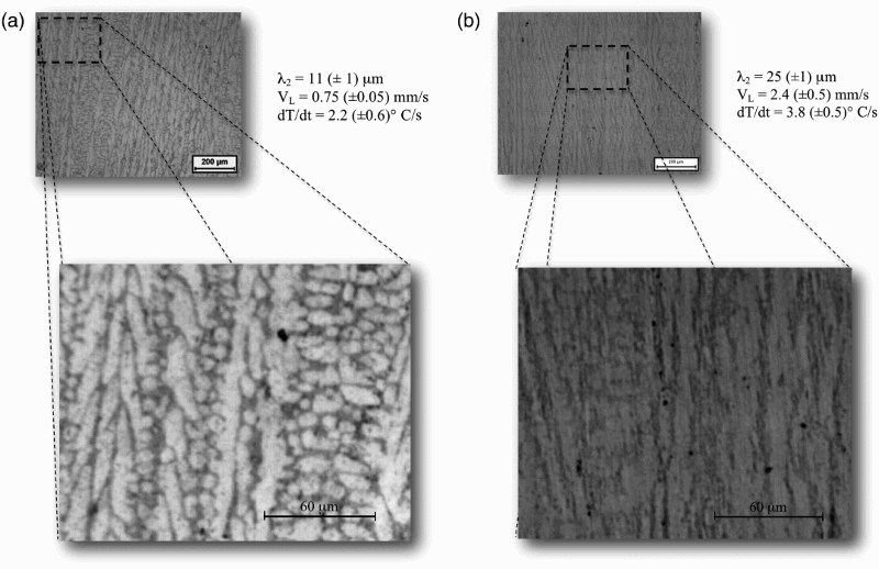
Since λ2 was determined as a function of both TCL and SA, it can also be related to their corresponding UTS, which have been previously reported.
8
The trend of UTS and SA versus λ2 for both Sn–2 wt-%Ag and the Sn–40 wt-% Bi alloys are shown in Fig. 7
a and 7b, respectively. It can be seen that for the Sn–Ag alloy with the increase in λ2, UTS decreased and the corresponding SA increased. Such combined plot mechanical strength versus wettability are being proposed because for engineering applications there is always a great concern in achieving improvements in a specific property without provoking any deleterious effects in another property. It can also be seen that the best combination UTS/SA is that corresponding to λ2 ∼9 μm, which is achieved under dT/dt of 4°C s−1.
The correlation: a and b UTS/SA, c and d UTS/TLC versus λ2, and wettability/strength correlation represented by: e TLC = f(UTS) and f SA = f(UTS) for the alloys examined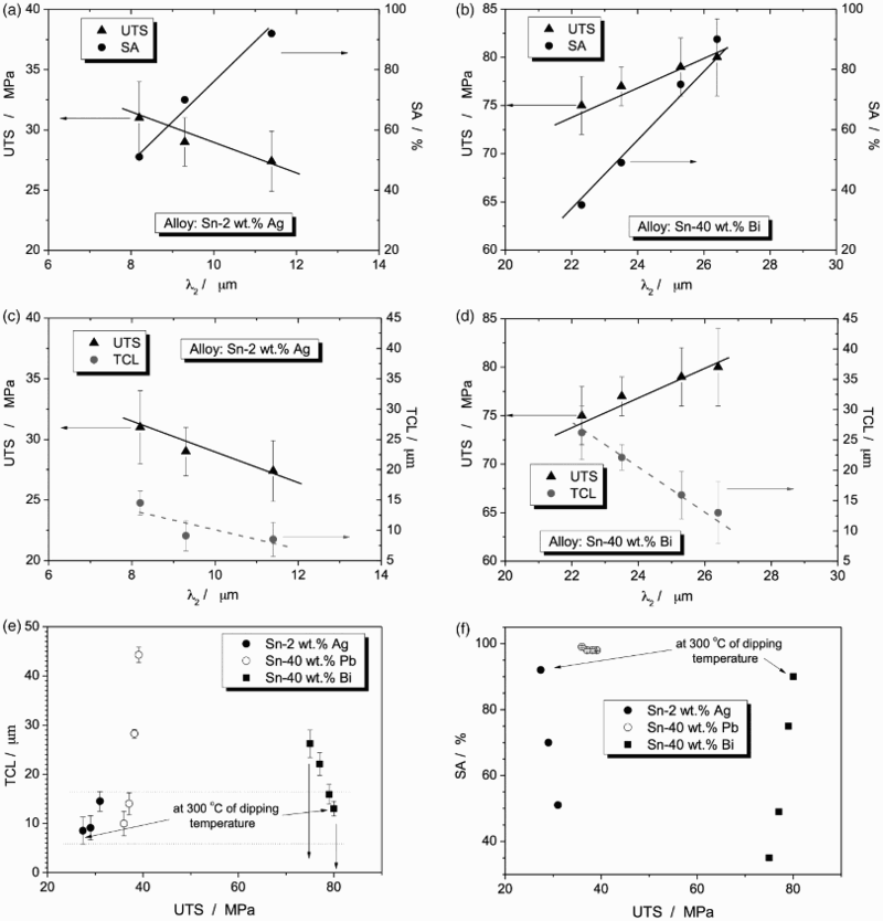
With respect to the Sn–40 wt-% Bi alloy (Fig. 7 b), it is found that the increase in λ2 is associated with increase in both UTS and SA. For a range of λ2 between 25 and 27 μm, a best combination UTS/SA for this Sn–Bi alloy is attained. This reflects a microstructure scale provided by dT/dt of about 2°C s−1. Based on the aforementioned assertions, it can be concluded that when an optimised combination UTS/SA is aimed, a faster solidification rate has to be provided (i.e. higher dT/dt), considering the Sn–2 wt-% Ag alloy. On the other hand, when combined results UTS/SA for the Sn–Bi alloy are considered, a slower dT/dt is better indicated. In order to attain the combined properties mechanical strength/wettability using a conventional soldering process, it means that a difference ∼2× in dT/dt should be applied.
As aforementioned, it is well-know that the control of the cooling rate in an industrial soldering is not ever easy. It is also known that distinct circuits and components are applied in SMT, THT or hybrid soldering technologies. However, it is believed that, for instance, in a reflow oven, considering a systematic experimentation correlating type of component in circuit and the selected solder alloy, the cooling rate can be reasonably controlled. It is also true that reflow, wave and manual soldering are potentially used in industry. On one hand, the wave soldering is cheaper and simpler than reflow, on the other hand, its temperature profile is non-linear and the control of cooling rate can be negatively affected. In this sense, it seems that controlling the temperature and time in the reflow stage as a function of a determined type of circuit or component's family, permits the cooling rate to be estimated. It is important to remark that excessive time and temperature can induce the growth of intermetallics leading to undesirable brittleness.
Figure 7 c and 7d plot UTS and TCL versus λ2 for both Sn–Ag and Sn–Bi alloys. Since TCL and SA have an opposite behaviour with λ2, it was expected that the Sn–Ag solder alloy would exhibit UTS and TCL decreasing with the increase in λ2. In contrast, the Sn–Bi alloy has evidenced a distinct behaviour concerning the evolution UTS versus λ2, that is, UTS increased with the increase in λ2. This has been previously reported, and explained, based on the onset of tertiary dendritic branches, which contributed for a more complex dendritic arrangement inducing a slight proportional increase in UTS. 8
Figure 7 e and 7f shows the wettability/tensile strength correlation for the Sn–Ag and Sn–Bi alloys examined compared with the traditional Sn–40 wt-% Pb solder. The wettability is represented by both TCL and SA. Figure 7 e evidences the TCL = f(UTS) for the three alloys. It is found that any alloy examined has its lower TCL associated with T = 300°C. Although the Sn–Bi alloy is shown to have a thicker TCL (∼30 μm), as compared to that of the Sn–Ag alloy when the lowest T is applied (<250°C), the highest UTS achieved (∼80 MPa) is that of the Sn–Bi solder alloy. These values are at least 2× higher as compared with those of the two other alloys examined. On the other hand, the conventional Sn–Pb alloy recorded the highest TCL (∼45 μm), and UTS ∼40 MPa. The smallest UTS and TCL are those of the Sn–Ag alloy.
Figure 7 f depicts the experimental results of SA = f(UTS). Considering the UTS results, a similar conclusion can be drawn to that associated with the results of Fig. 7 e. However, the SA/UTS correlation provides important information concerning the association wettability/mechanical strength, with consequences to the quality of soldering joints. It is found that the proposed Sn–Bi alloy can be an excellent alternative to the Sn–Pb solder when the wettability represented by SA >70–80% associated with higher tensile strength (2× higher than Sn–Pb alloy) is needed. It is worth noting that the ductility has an important role on long-term reliability of solders. At a range of temperatures from 90 to 120°C during the cycle-life, due to atomic diffusion, the ductility of a solder can significantly be affected, which directly also affects the corresponding strength. Based on the fact the ductility/wettability correlation can also be demanded in some applications, the elongation to fracture (δ) as a function of parametric features of the resulting microstructure of Sn–Ag and Sn–Bi solder alloys has been previously examined.8, 9
Although the Sn–Bi solders have a more brittle behaviour when compared with some other solders, it was shown 9 that a Sn–40wt-% Bi alloy has its elongation (δ) varying with the scale of the microstructural matrix (i.e. the dendritic spacing, λ2). It was found that the elongation varied from ∼15 to ∼20%. When λ2 was about 10 μm, the elongation attained a value about 15%. For coarser microstructures the elongation reached up to 20%. Considering the Sn–2 wt-% Ag alloy, the elongation was shown to be about 36∼38% for a λ2 of 40 μm. In contrast, the lowest value of δ was found to be 22∼23% for a dendritic array having λ2 about 24∼25 μm. For comparison purposes, if a same range of λ2 is considered, the examined Sn–Ag solder was shown to have the elongation in the range 25–32%, while that of the Sn–Bi solder was associated with 15–20%.8, 9 However, this does not mean necessarily a deleterious effect for the selection of the Sn–Bi alloy, because in this same range of λ2 this alloy was shown to have the best UTS/SA combination, associated with a cooling rate of 2°C s−1.
The Sn–Ag alloy is characterised by good/excellent SA obtained at T >250°C, high UTS (up to 30 MPa) and elongation ≥40%. 8 Additionally, both the relative cost and weight with respect to Sn–Pb alloy should also be considered. In a previous investigation 8 it was reported that the Sn–Ag alloy has a relative cost that is higher than those of both Sn–Pb and Sn–Bi alloys.
Conclusions
From the present investigation the following conclusions can be drawn:
It was found that both the Sn–2 wt-%Ag and Sn–40 wt-%Bi alloys tend to have TCL in a Cu substrate decreasing with the increase in T, as also previously reported for the Sn–Pb alloy. For T >250°C, a quite similar TCL has been observed for all solder alloys examined, including the traditional Sn–Pb alloy. It was shown that both the Sn–Ag and Sn–Bi alloys have SA increased with the increase in T. The better wettability behaviour represented by SA >70% is attained for T >250°C. The highest SA was shown to occur for T = 300°C for both Sn–Ag and Sn–Bi alloys. Besides, it can also be concluded that the combination highest SA/TCL is attained for ∼300°C. TCL and SA have opposite behaviour with respect to both dT/dt and λ2. The Sn–Bi alloy was shown to have lower SA values than those of the Sn–Ag alloy for similar dT/dt ranges. For the Sn–Ag alloy, it was found that UTS and SA decreased and increased with the increase in λ2, respectively. The best combination UTS/SA has been evidenced for λ2∼9 μm. This means that dT/dt∼4°C s−1 should be applied during soldering. The corresponding elongation was reported to attain up to 32–34%.
8
Considering the Sn–Bi alloy, it was shown that with increasing λ2 both UTS and SA increase. The best combination UTS/SA it is attained for λ2 of 25∼27 μm, that is, associated with dT/dt∼2°C s−1. The corresponding elongation for this same range of microstructural scale was shown to be about 20%.
9
When the wettability–tensile strength correlation was established in terms of SA/UTS, it was clearly evidenced that the Sn–Bi solder attained SA >70–80% associated with the highest UTS of all solders examined, that is, 2× higher than that of the traditional Sn–Pb alloy. The Sn–Bi alloy has a relative cost that is similar to those of both the traditional Sn–Pb and the eutectic Sn–Zn alloys. These assertions can be used as guidelines for an appropriate material selection. It is evident that ductility should also be meticulously analysed when this property is relevant to a particular application, for example, for systems requiring long-term reliability and those in which the working temperature can be relatively higher than that of conventional systems.
Footnotes
Acknowledgements
The authors acknowledge FAEPEX-UNICAMP, and CNPq (The Brazilian Research Council, Grants 305502/2014-0 and 446797/2014-6).