
Abstract
Ti–Al bimetallic components present extensive application prospects and have attracted considerable attention owing to their low cost and light weight. In this study, Ti–Al bimetallic structures with one, two, and five Al layers were fabricated via wire and arc additive manufacturing by cold metal transfer welding. During the deposition process of the first Al layer, the matrix was TiAl, and a needle-shaped Ti3Al was formed. Subsequently, from the second deposition layer of the Al alloy, however, TiAl3 was formed, and it exhibited an exceptional morphology with two types of structures: coarse columnar grain structures with identical growth orientation, and long strip-like structures with a random distribution. The formation order of Ti–Al intermetallic compounds was TiAl3, TiAl, and Ti3Al.
Keywords
Introduction
In general, a bimetallic structure has been fabricated using an additive manufacturing technique. Using laser deposition technology, the bimetallic structure was fabricated from Ti–6Al–4V to Invar [1]. The bimetallic structure of Inconel 718-GRCop-84, direct deposition of GRCop-84 on Inconel 718, and compositional gradation of two alloys were successfully fabricated using laser-engineered net shaping technology [2, 3]. A compositionally graded 100% Ti to 100% Al alloy structure was fabricated using laser-engineered net shaping technology with Ti6Al4V + Al12Si powders [4]. However, recently, wire and arc additive manufacturing (WAAM) techniques have been employed to fabricate bimetallic components to enhance manufacturing efficiency. The WAAM technique, a three-dimensional (3D) printing method based on an incremental layer-by-layer manufacturing process using a digital model [5] is regarded as a promising manufacturing process. During the fabrication process, an electric arc is used as the heat source and a welding wire is used as the feeding material [6, 7]. Owing to the high arc energy input, a large-scale component with full density and complexity is obtained by WAAM, which is a significant option for structural materials [8]. WAAM offers numerous advantages, such as a high material utilisation rate, high production rate, low equipment cost, and consequent environmental friendliness [9-11]. WAAM has been widely accepted in diverse industries, such as automotive, healthcare, energy, and aerospace fields for the manufacturing of metallic components [12-15]. No defects were found near the interface of the bimetallic stainless steel-nickel-based alloy fabricated via WAAM [16]. The WAAM technology was employed to fabricate a bimetallic structure of austenitic stainless steel, SS904L, and Hastelloy C-276 by feeding ER904L and ERNiCrMo-4 filler wires [17]. In a previous study, the WAAM technology has been used to successfully fabricate a bimetallic Fe3Ni–FeNi structure with a hot cracking defect [18].
A Ti–Al bimetallic component possesses the advantages of both Ti and Al alloys, such as light weight and low cost [19], thereby presenting extensive application prospects. The Ti–Al bimetallic structures are used in the aerospace, aviation, automobile, and transport industries owing to their prominent corrosion-resistant and light-weight properties [20, 21]. However, research on Ti–Al bimetallic structures fabricated by WAAM technology is limited and thus requires further research.
In a previous study, the deposition order of Ti and Al wires was studied [22]. The first use of Ti wire was favourable for the fabrication of Ti–Al bimetallic structures. For Ti–Al bimetallic structures, the Ti/Al reaction layer was a brittle area. During the fabrication process, the deposition layer of the Al alloy had an influence on the Ti/Al reaction layer. In this study, bimetallic structures of Ti–6Al–4V and Al–6.25Cu alloys with different deposition layers of Al alloy were fabricated using WAAM by cold metal transfer (CMT) welding. The primary objective of this study is to investigate the effects of Al alloy deposition layers on the microstructure characterisation of the reaction layers of the Ti–Al bimetallic structure.
Experiments
Chemical compositions of the filler wires and substrate (wt-%).
Deposition parameters of deposition process.
After obtaining the Ti–Al bimetallic structures, metallographic specimens were cut, polished, and etched for approximately 1 min using a standard Keller solution. The generated phase of the reaction layer was determined via D8 advanced X-ray diffraction (XRD). The microstructures of the metallographic specimens were observed via optical microscopy (OM; OLYMPUS GX51), scanning electron microscopy (SEM) coupled with energy dispersive spectroscopy (EDS; Hitachi S-4800), and transmission electron microscopy (TEM; FEI Tecnai F30). The TEM positions of samples 1, 2, and 3 are indicated by the red circles in Figures 1, 6, and 11, respectively. The TEM specimens with a thickness of 0.5 mm and diameter of 3 mm were cut by wire-cut electrical discharge machining and grounded to 50 µm. Subsequently, the specimens were pasted into a pitting meter and mechanically thinned to approximately 10 µm. Finally, ion thinning was applied to the TEM specimens.
OM images of reaction layer morphology in sample 1 (the red circle is the selected TEM position).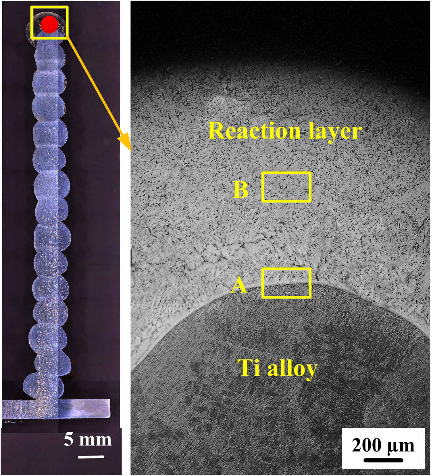
Results
Microstructure analysis of sample 1
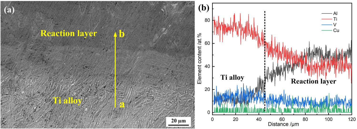
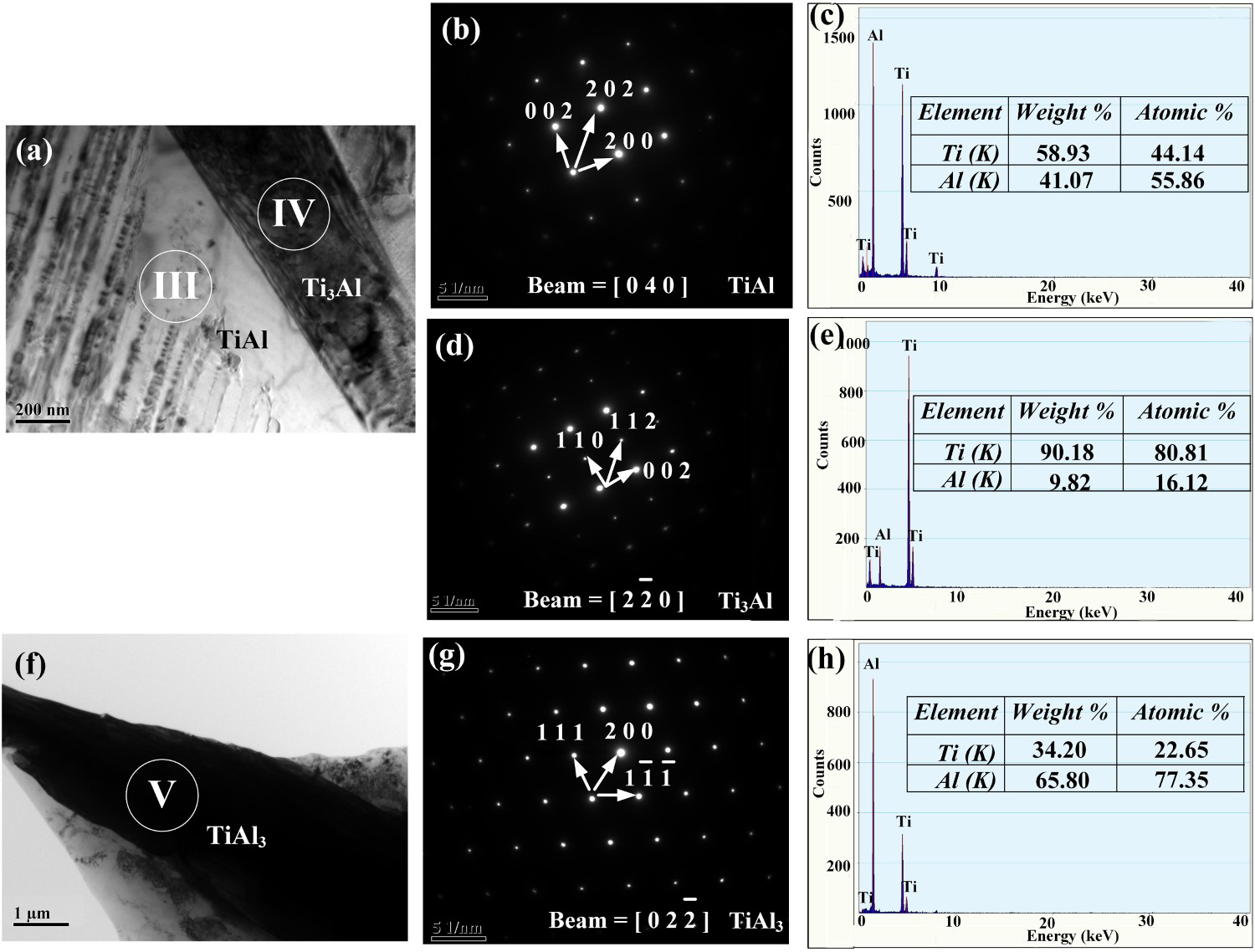
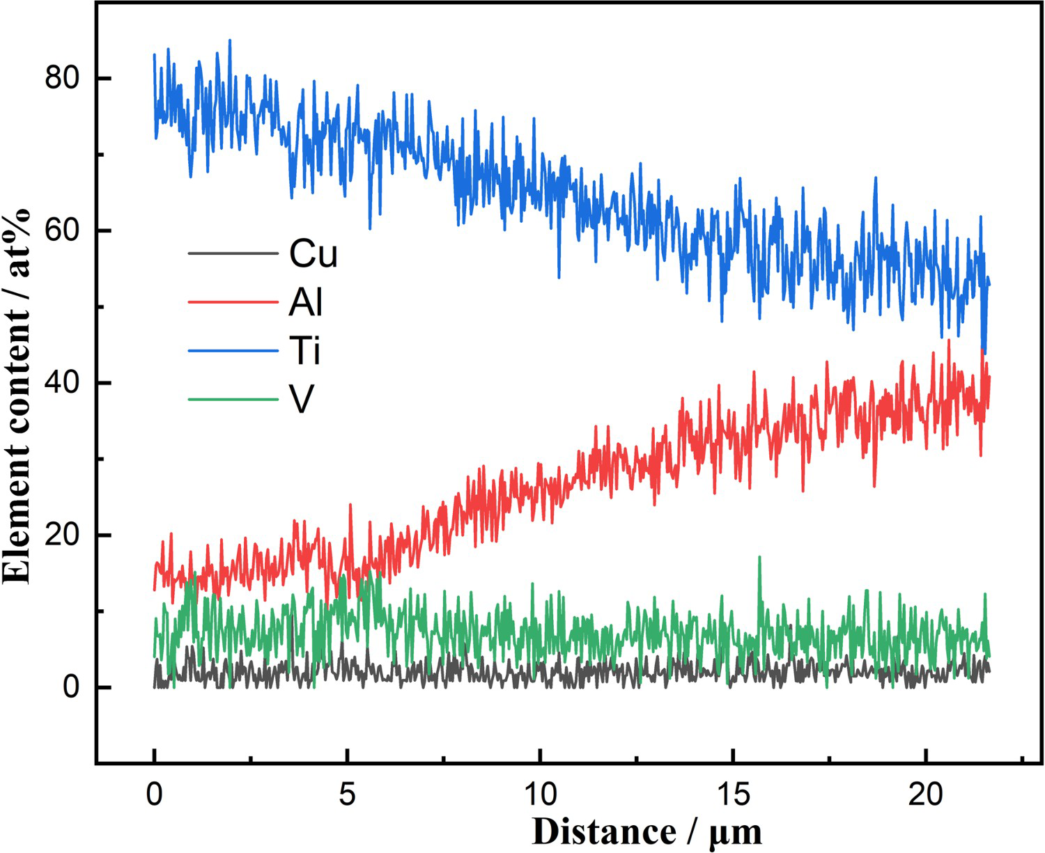
In Figure 1, the edge morphology of the last Ti layer is not regularly round. Compared with the previously deposited Ti layers, the volume of the last Ti layer was significantly reduced. This indicates that the last Ti layer melted during the first Al layer deposition process, which led to a reaction between the Ti and Al atoms. Based on the microstructure morphology, the build component of sample 1 was divided into two areas: A and B. In area A, the interface was clear, and a Ti/Al reaction layer was formed above the interface. In Figure 2, from a to b, the elemental composition of Ti and Al changed dramatically, that is, the composition of Ti and Al decreased and increased, respectively. Near point a, the microstructure revealed a basket-weave structure. Combined with EDS line scanning analysis, the basket-weave structure was found to be Ti alloy [23]. In Figure 2(b), the element composition ratio of Ti and Al is approximately 1:1 in the reaction layer, which indicates that the microstructure near point b is the TiAl phase.
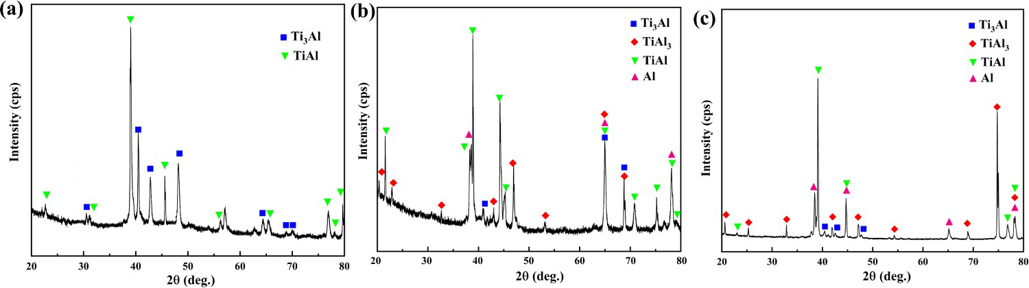
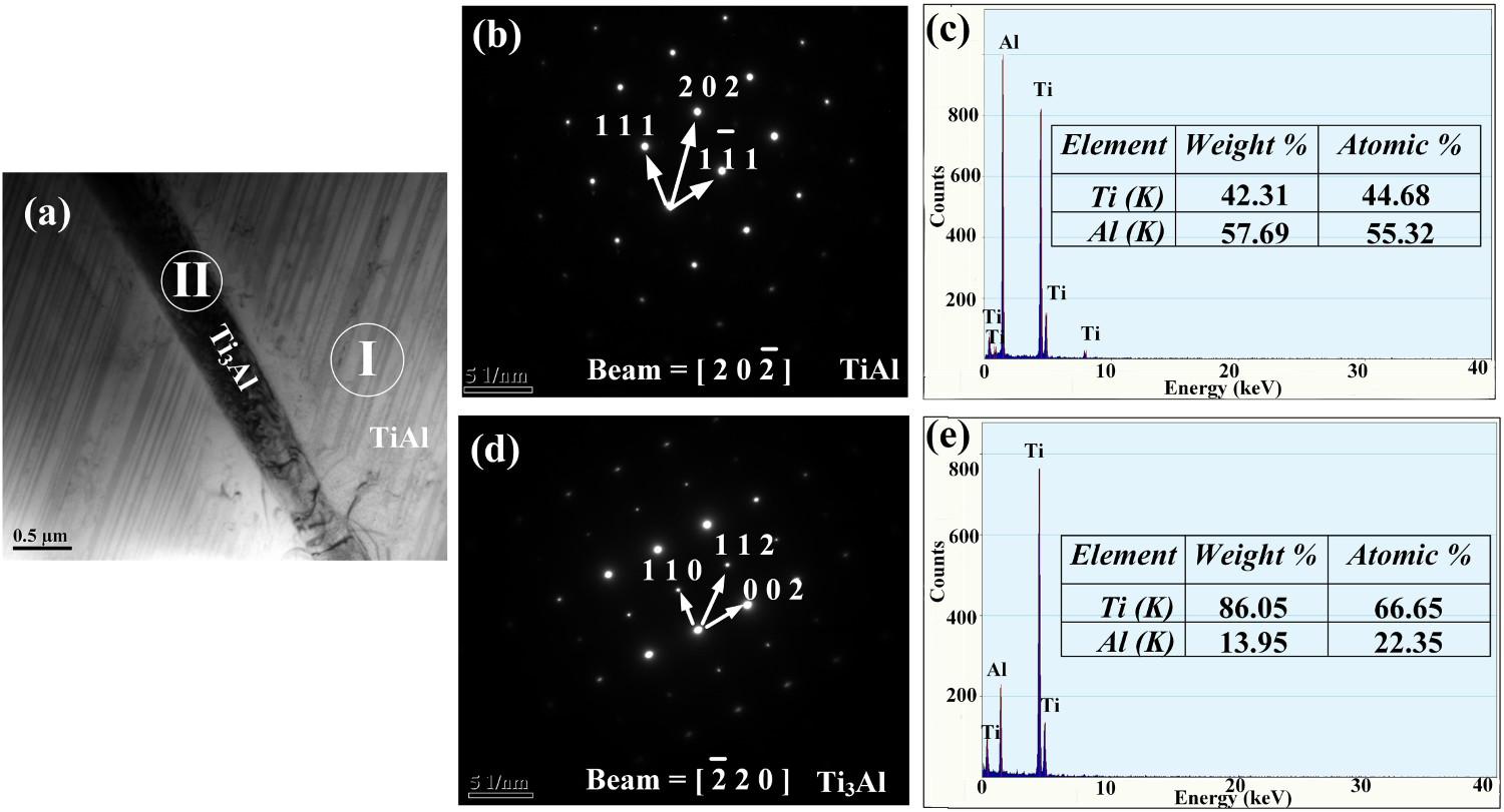
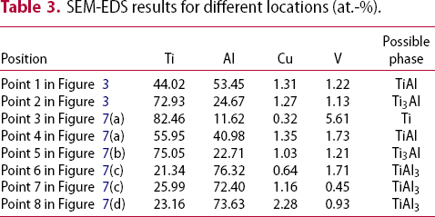
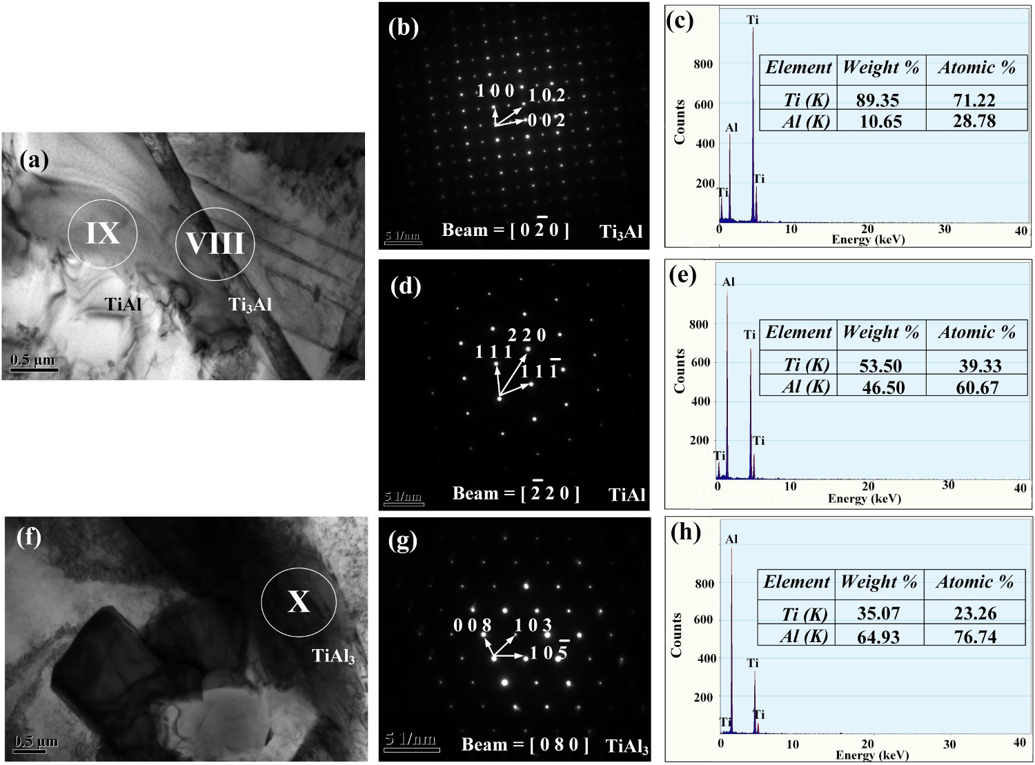
According to the SEM-EDS results in Table 3, the matrix was TiAl (Figure 3), and a needle-like phase with a length of 30 µm was formed, which was identified as Ti3Al. Figure 4(a) shows the XRD results of the reaction layer in a sample where only TiAl and Ti3Al were detected. The dominant peak was TiAl, which was identified as the matrix. The phase composition was confirmed by TEM, and the results are shown in Figure 5. According to the results of the electron diffraction pattern and corresponding TEM-EDS, the matrix was TiAl, and the needle-like phase was Ti3Al in area B. The results of the TEM analysis were similar to those obtained by SEM-EDS. The Ti3Al and TiAl phases decreased to the component top. Therefore, the reaction layer was composed of Ti3Al and TiAl phases when Al alloy with only one layer was deposited.
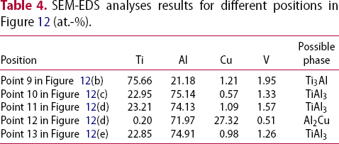
Microstructure of rectangle B in Figure 1. XRD results of reaction layer: (a) sample 1, (b) sample 2 and (c) sample 3. TEM analysis of area B of sample 1: (a) TEM image, (b) electron diffraction pattern of area I, (c) TEM-EDS result of area I, (d) electron diffraction pattern of area II and (e) TEM-EDS result of area II. SEM-EDS results for different locations (at.-%). SEM-EDS analyses results for different positions in Figure 12 (at.-%).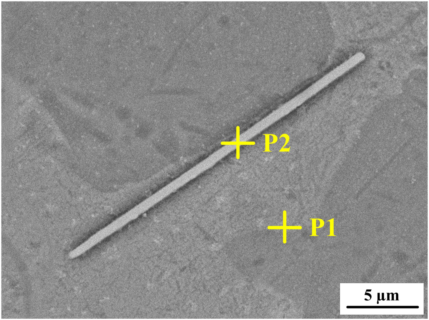
Microstructure analysis of sample 2
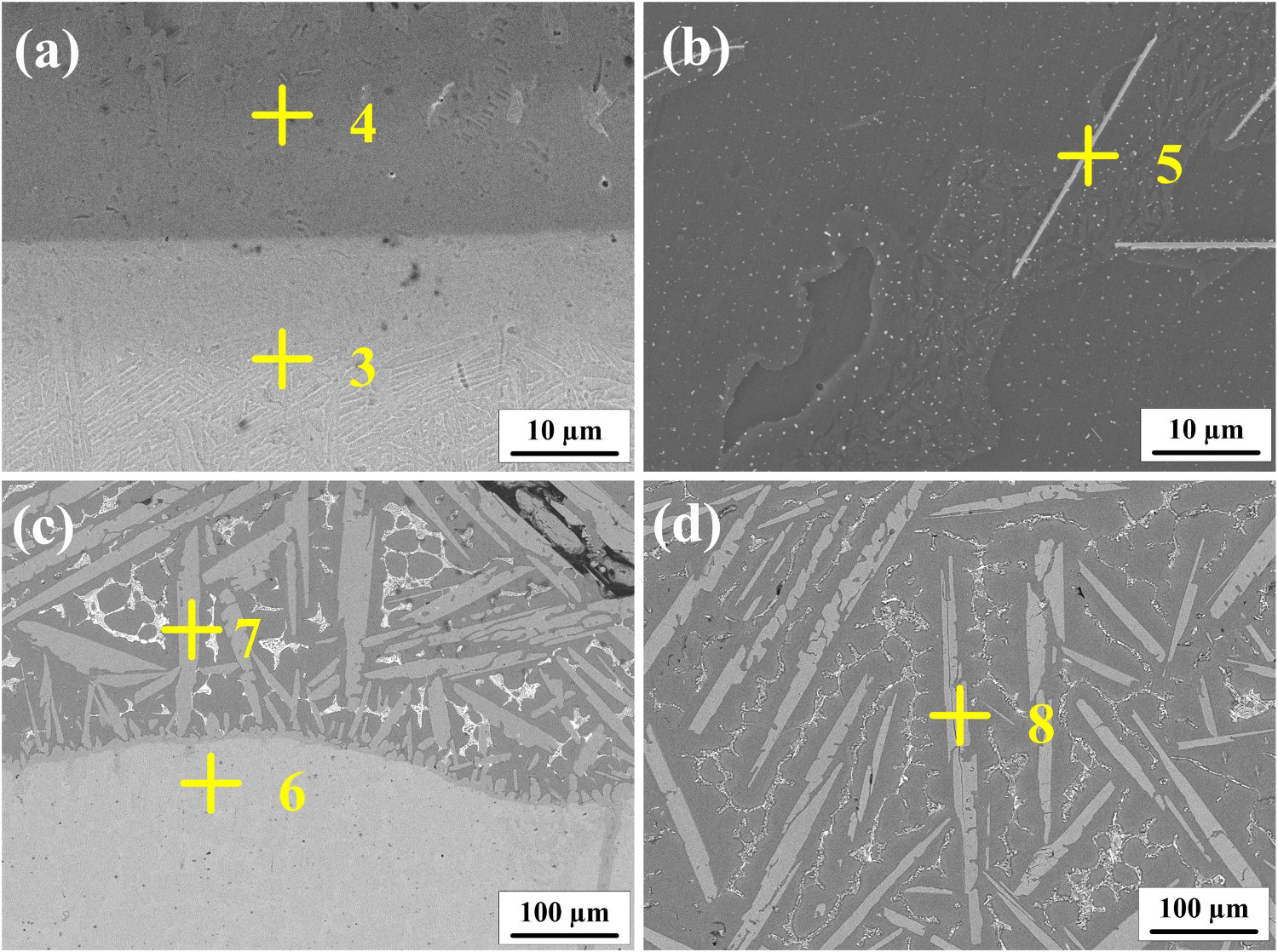
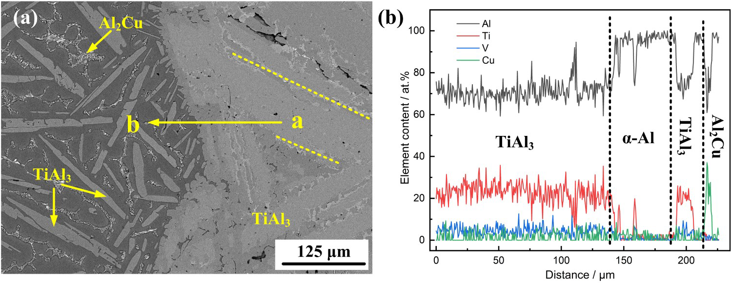
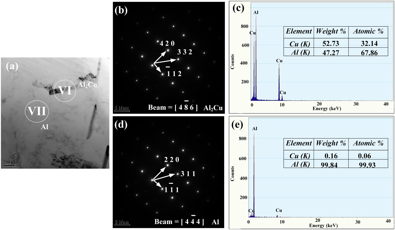
In Figure 6, a component is divided into four areas, and the corresponding microstructures of different areas are shown in Figure 7. In area A, the interface is depicted in Figure 7(a). According to the EDS results of points 3 and 4, in area A, the bottom layer was Ti alloy and the upper layer was TiAl phase. In Figure 7(b), in area B, a needle-like phase was formed, which was later confirmed to be Ti3Al from EDS analysis of point 5. The microstructure morphologies of areas A and B in sample 2 were similar to those in sample 1. In area C, the interface was apparent, and the bottom and upper microstructure morphologies were significantly different. The different microstructure morphologies at the bottom and upper parts of area C were found to be TiAl3 from EDS studies. In Figure 7(c), at the upper part of area C, the shape of TiAl3 was a long strip with a length of 50–200 µm and a width of 2 µm, and a white net structure phase was generated. In addition, Figure 8(a) shows the amplified microstructure of area C, and according to Figure 8(b), near point a, the atomic ratio of Ti:Al was approximately 1:3, similar to the result of point 6, which was confirmed to be TiAl3. According to Figure 8(b), at the upper part of area C, the white net structure phase was Al2Cu and the matrix was α-Al. In Figure 4(b), in the reaction layer, Ti3Al, TiAl, Ti3Al, and α-Al were detected according to the XRD results. However, the Al2Cu phase was not detected because of the low content of the Al2Cu phase in the reaction layer. Figure 9 shows the TEM analysis of areas B and C of sample 2. In Figure 9, the needle-like portion corresponded to Ti3Al, the matrix was TiAl, and the coarse long strip was TiAl3. The results of the TEM analysis were in accordance with those of the corresponding SEM-EDS. According to the result of point 8 in Figure 7(d), the TiAl3 phase in the long strip shape was still formed in area D. TiAl3 continued to grow to the top of the component. The length of TiAl3 was approximately 600 µm. The length of TiAl3 decreased with an increase in the distance from the Ti/Al interface. According to the TEM electron diffraction pattern and TEM-EDS in Figure 10, α-Al and Al2Cu as a second phase were found in areas D and α-Al, respectively.
OM images of reaction layer morphology in sample 2 (the red circle is the selected TEM position). Microstructure of rectangles in Figure 6: (a) area A, (b) area B, (c) area C and (d) area D. EDS line scanning of area C in Figure 6: (a) microstructure and (b) EDS line scanning results from a to b. TEM analysis of areas B and C in sample 2: (a) TEM image, (b) electron diffraction pattern of area III, (c) TEM-EDS result of area III, (d) electron diffraction pattern of area IV, (e) TEM-EDS result of area IV, (f) TEM image, (g) electron diffraction pattern of area V and (h) TEM-EDS result of area V. TEM analysis of areas D in sample 2: (a) TEM image, (b) electron diffraction pattern of area VI, (c) TEM-EDS result of area VI, (d) electron diffraction pattern of area VII and (e) TEM-EDS result of area VII.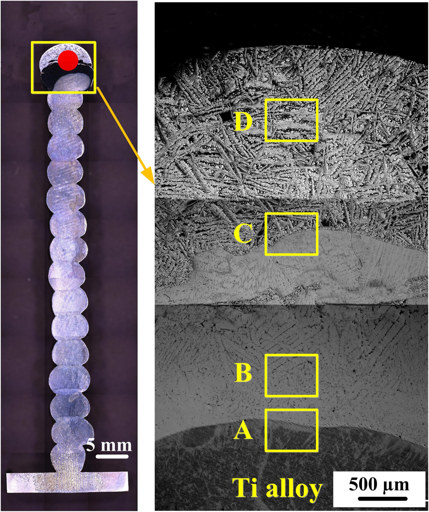
Based on the above analysis, the reaction layer in sample 2 primarily comprised Ti3Al, TiAl, and TiAl3 phases when two layers of Al alloy were deposited. In addition, α-Al and Al–Cu eutectic structures were formed at the top of the component.
Microstructure analysis of sample 3
In Figure 11, for sample 3, the component is divided into six areas. In Figure 12(a), in area A, the interface between the last Ti layer and the reaction layer is clear. In Figure 13, from point a to point b in Figure 12(a), the Ti content decreased and the Al content increased. Near point b, the atomic ratio of Ti:Al was approximately 1:1. Therefore, in Figure 12(a), near point b, the microstructure is TiAl. According to the EDS line scanning analysis in Figure 13, the microstructure near point a was Ti alloy [24]. A needle shape was formed in area B, as shown in Figure 12(b), which was confirmed to be Ti3Al. The scope of area B was approximately 600 µm. As shown in Figure 12(c), TiAl3 was formed along the TiAl phase in area C. In Figure 4(b), in the reaction layer, XRD results indicated the presence of Ti3Al, TiAl, and Ti3Al of Ti–Al compounds. In Figure 14, the TEM analysis indicated that Ti–Al IMC, such as Ti3Al, TiAl, and TiAl3, were formed in sample 3. The results of the TEM analysis were consistent with those of the SEM-EDS analysis and XRD.
OM images of reaction layer morphology in sample 3 (the red circle is the selected TEM position). Microstructure of rectangles in Figure 11: (a) area A, (b) area B, (c) area C, (d) area D, area E and (f) area F. EDS line scanning analysis from points a to b in Figure 12(a). TEM analysis in areas B, C and D of sample 3: (a) TEM image, (b) electron diffraction pattern of area VIII, (c) TEM-EDS result of area VIII, (d) electron diffraction pattern of area IX, (e) TEM-EDS result of area IX, (f) TEM image, (g) electron diffraction pattern of area X and (h) TEM-EDS result of area X.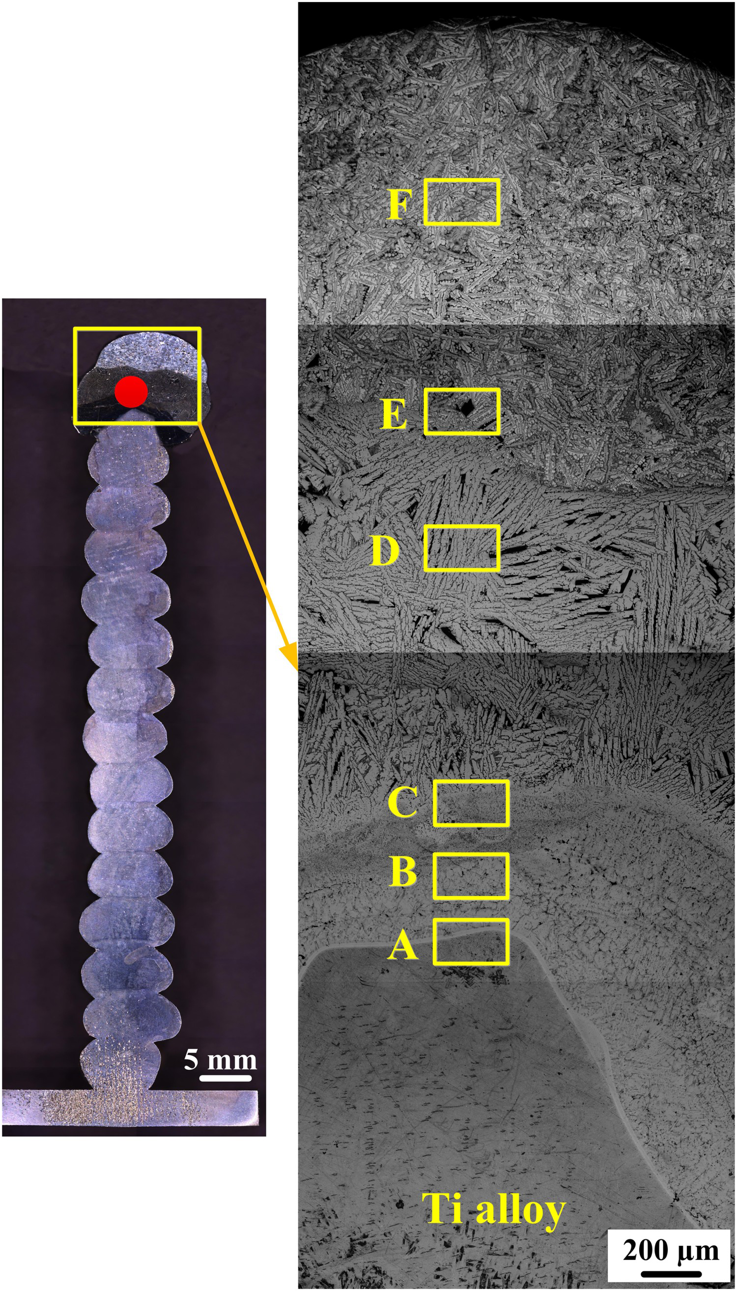
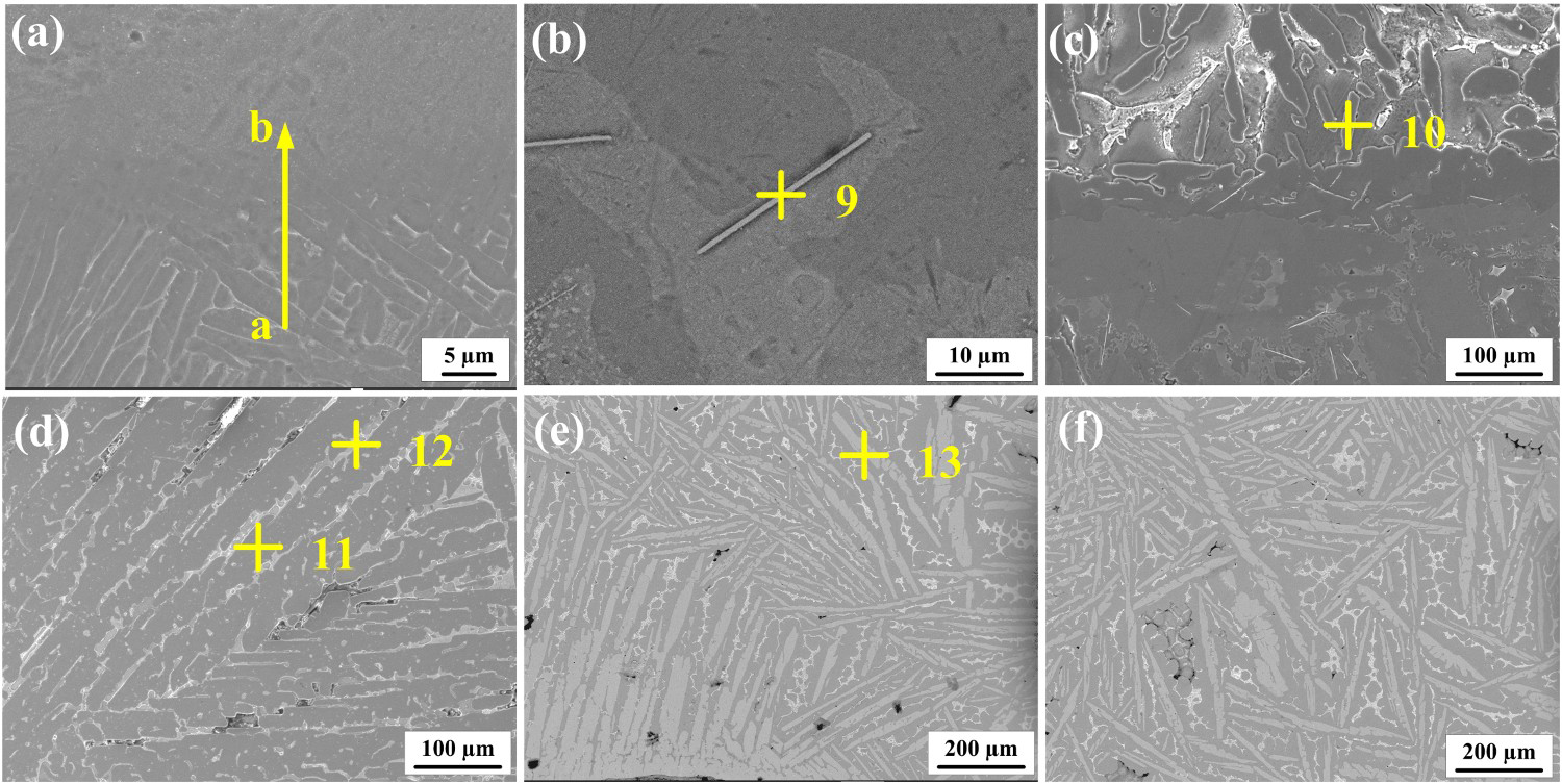
According to the EDS results of points 11 and 12 in Figure 12(d), Al2Cu with a white net shape was formed between the adjacent TiAl3 phase in area D. As shown in Figure 12(e), coarse TiAl3 grew along the same direction. TiAl3 having dimensions of 600 µm length and approximately 50 µm width was distributed randomly in area D. In area E, the strip was TiAl3, and parallel and randomly distributed TiAl3 existed simultaneously. The microstructure, from area D to F, evolved from parallel TiAl3 to completely random TiAl3. In area F, parallel TiAl3 was not formed. In area F, the length of TiAl3 was approximately 300 µm. The distribution of TiAl3 in area F was approximately 2.5 mm. At the component top, TiAl3 still existed. Overall, the microstructure morphology and distribution in sample 3 were similar to those in sample 2.
Discussion
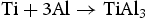
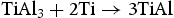
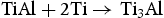
As mentioned, during the first layer deposition process of the Al alloy, the last layer of the Ti alloy melted significantly leading to mutual diffusion between Ti and Al atoms. According to Ti–Al binary phase diagram [25, 26], different kinds of Ti–Al IMC, including Ti3Al, TiAl, TiAl3, TiAl2, and Ti2Al5, are formed. However, for the Ti–Al IMC, only three phases can exist stably: Ti3Al, TiAl, and TiAl3 [27]. In this study, only Ti3Al and TiAl were found in area B of sample 1, and the other IMC types were not detected by XRD and TEM. Compared with the Gibbs free energy of formation for Ti3Al and TiAl, the energy needed for the formation of TiAl3 was relatively low [27-30]. Therefore, the formation order of the TiAl3 phase was higher than those of Ti3Al and TiAl. However, for sample 1, the Ti–Al IMC formation order of the computation result was contradictory to that of the experimental result. In practice, for sample 1, Ti and Al atoms reacted, which led to the formation of the TiAl3 phase initially [31]. Xu [28] reported that the early stages of the phase reaction between Ti and Al were characterised by the initial formation of TiAl3 for any composition and temperature up to the melting point of Al. However, TiAl and Ti3Al phases were not detected at the early stage [32]. The first reaction between Ti and Al atoms occurred, as shown in Equation (1), which led to the formation of TiAl3. After the formation of TiAl3 phase, Al atoms were consumed, and some of the Ti atoms remained unreacted. At high temperatures, as shown in Equation (2), TiAl3 and Ti atoms reacted to form TiAl [33]. And TiAl was the matrix. After the formation of TiAl, Ti atoms remained intact, which later reacted with Ti atoms and formed Ti3Al with a needle-like structure. The reaction is shown in Equation (3). The distribution of TiAl and Ti3Al was from the interface to the top of the component. Sina et al. [34] reported that the initially formed TiAl3 was a metastable phase that disappeared upon further heating due to the reaction with unreacted Ti atoms. Luo et al. [35] reported that TiAl3 was formed as the first phase, and TiAl as the second in the Ti–Al IMC if all the Al atoms were consumed, followed by the formation of Ti3Al, which grew together with TiAl3 and TiAl until the terminal phases were consumed. The results of this study are similar to those reported by Luo et al. and Sina et al.
For samples 2 and 3, TiAl3, TiAl, and Ti3Al phases were detected according to the results of XRD and TEM. Compared with the thickness of TiAl formed in sample 1, the thickness of samples 2 and 3 diminished, which indicated the possibility of TiAl being remelted during the deposition of the second layer of Al alloy in samples 2 and 3. From SEM and XRD studies, the TiAl3 phase was detected during the deposition of the second layer, which underwent heterogeneous nucleation along with the TiAl phase owing to the availability of Al atoms. However, Ti3Al and TiAl phases were not detected at the top of the component in samples 2 and 3. In other words, Ti-rich compounds such as TiAl and Ti3Al were not formed during the reaction in excess Al. The morphology and distribution of TiAl IMC (TiAl3, TiAl, and Ti3Al) fabricated by WAAM technology was significantly different from that of other technologies owing to the unique layer-by-layer deposition method.
According to the above analysis, the TiAl3 phase was formed first. However, in the area with a high concentration of Ti atoms, the reaction between TiAl3 and Ti occurred, which led to the formation of TiAl and Ti3Al phases. An increase in the number of Al atoms with an increase in the Al deposition layer suppressed the reaction between TiAl3 and Ti. From the second Al layer, a TiAl3 phase with different morphology was formed. The TiAl3 phase grew to the as-built component top with five deposition layers of the Al alloy. Therefore, the formation order of Ti–Al IMC was TiAl3, TiAl, and Ti3Al.
Conclusions
In this study, Ti–Al bimetallic structures with different deposition layers of Al alloy were obtained by WAAM using the CMT technology. The effects of the Al alloy deposition layers on the reaction layer microstructure of the Ti–Al bimetallic structures were studied. The main conclusions are as follows:
During the deposition of the first layer of Al alloy, the matrix was TiAl, and a needle-shaped Ti3Al was formed in the second phase. Following the deposition of the second layer of Al alloy, TiAl3 with a long stripe shape was formed. The morphology of TiAl3 included two types of layers: coarse columnar grain structures with the identical growth orientation, and long strip-like structures with a random distribution. With an increase in the number of deposition layers, the thickness of IMC increased. In addition, the amount of TiAl3 increased significantly. TiAl and Ti3Al did not exist in the area of TiAl3. The formation order of Ti–Al IMC was TiAl3, TiAl, and Ti3Al.
Footnotes
Disclosure statement
The authors declare no competing interests.
Author contribution
Yinbao Tian: Data curation, Formal analysis, Writing - original draft. Junqi Shen: Funding acquisition. Shengsun Hu: Resources, Xinya Chen: Writing - review. Yangchuan Cai: Methodology. Jian Han: Investigation, Methodology and editing.
Consent to participate
All the authors have approved to participate in the manuscript.