
Abstract
Frictions stir welding (FSW) and ultrasonic vibration enhanced FSW (UVeFSW) of dissimilar Al/Mg alloys were conducted, and the intermetallic compounds (IMCs) layers formed at Al/Mg interface in welds were characterised by TEM. It was found that the IMCs thickness was significantly reduced in UVeFSW, and the IMCs were generated by solid-state atomic diffusion in butt joints under the used welding conditions since the measured temperature at the tool/workpiece interface was far below the eutectic points. The EBSD characterisation showed that ultrasonic vibration improved the degree of grain recrystallization on both sides of the IMCs layers and promoted the consumption of dislocations, which resulted in a reduced diffusion rate of atoms. Therefore, the growth of IMC layer was suppressed in UVeFSW.
Introduction
Dissimilar aluminium/magnesium (Al–Mg) components provide many opportunities for manufacturing lightweight structures with multi-functionalities. However, the joining of Al alloy to Mg alloy causes the formation of detrimental intermetallic compounds (IMCs) at the Al–Mg interface. Although friction stir welding (FSW), as a solid-state process, can achieve good and defect-free joints of Al/Mg alloys, the unavoidable formation of IMCs in welds is always the main factor restricting the performance of the dissimilar joints [1-4].
In order to suppress the generation of IMCs and further improve the joint strength, some FSW process variants were developed, such as heat source assisted FSW [5], cooling assisted FSW [6], ultrasonic vibration-assisted FSW [3, 7, 8], etc. Previous investigations have proved that the ultrasonic vibration-assisted FSW process has advantages, such as inhibiting the growth of IMCs layers, promoting the material flow in the weld nugget zone (WNZ) and enhancing the mechanical interlock between Al and Mg alloys [7-10]. However, the underlying mechanism of ultrasonic vibration interaction with FSW process variables, especially the thinning mechanism for the IMC layer, still lacks a clear explanation.
In this study, in order to better understand the formation process of IMC layer and try to explain the thinning mechanism of IMC layer thickness by ultrasonic vibration, friction stir butt welding of Al alloy and Mg alloy was carried out. The temperature inside and outside the WNZ was measured. The microstructure of IMC layer and its surrounding grains was characterised and analysed by transmission electron microscope (TEM) and electron backscattered diffraction (EBSD). The changes in IMC layer and its surrounding microstructure before and after applying ultrasonic vibration were compared, and the action mechanism of ultrasonic vibration on the IMC layer was discussed.
Experimental details
In this study, 6061-T6 Al alloy plate and AZ31B-H24 Mg alloy plate were friction stir butt welded. The size of the plate used was 200 mm (length) * 60 mm (width) * 3 mm (thickness), and the nominal chemical composition was listed in Table 1 [9]. The tool made of H13 tool steel was with a concave shoulder (diameter 12 mm) and a cone-shaped pin with right-hand thread (length 2.75 mm, tip diameters 3.2 mm, root diameter 4.2 mm). The Mg alloy and Al alloy were placed on the advancing side (AS) and the retreating side (RS), respectively, and the pin was offset to the Mg alloy side by 0.3 mm. The following process parameters were selected in this study: the tool rotation speed of 800 rev min−1 and the welding speed of 50 mm min−1. The inclination angle of tool was 2.5°, and the plunge depth of shoulder was 0.15 mm. As schematically shown in Figure 1, ultrasonic energy was transmitted to the workpiece through the sonotrode with a tilt angle of about 40° between the horizontal plane. The ultrasonic vibration frequency was 20 kHz, and the power was 220 W. Conventional FSW and ultrasonic vibration enhanced FSW (UVeFSW) tests were made.
Schematic of the FSW and UVeFSW of dissimilar Al/Mg alloys and the TEM sampling location. Nominal composition and mechanical properties of base material.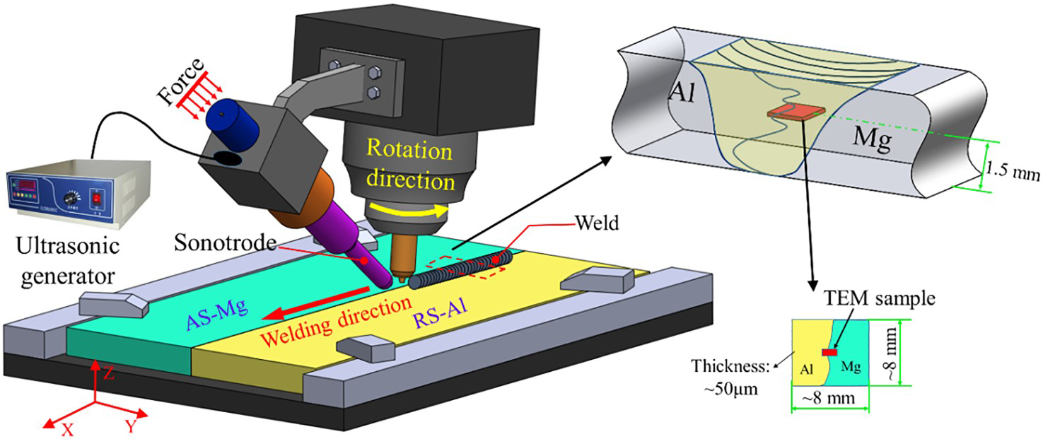
During the welding process, the temperature inside and outside the WNZ was measured. As shown in Figure 2(a), two K-type thermocouples were placed through the holes made on the tool, and the ends of the thermocouples were located on the bottom surface of the shoulder and the side surface of the pin, respectively. Combined with the wireless temperature measurement system [11], the material temperatures at the shoulder/workpiece and the pin/workpiece interfaces (points 1 and 2) were measured. For the temperature measurement outside the WNZ, a blind hole with a diameter 1 mm and depth of 1.5 mm was made on the Mg base metal (Advancing side), and one K-type thermocouple was planted at the hole bottom located 8 mm away from the tool axis, as shown in Figure 2(b).
Schematic diagram of thermocouple placement positions, (a) on the tool/workpiece interfaces, (b) on the Mg plate.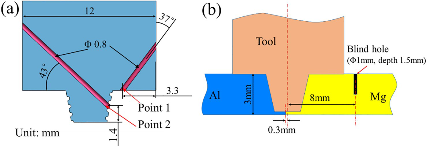
After welding, samples were cut at the centre of the weld (1.5 mm from the bottom of the weld, as shown in Figure 1) by a wire electric discharge cutting machine. After processing and polishing, the dimension of the samples for transmission electron microscope (TEM) was 8 mm in length, 8 mm in width and 50 µm in thickness. Finally, samples were cut by a focused ion beam (FIB) (Thermo Fisher Scios2). The IMCs on the Al/Mg bonding interface were characterised by FEI Tecnai G2 F20 TEM. For EBSD characterisation by field emission scanning electron microscope (FE-SEM) (Zeiss Gemini 500), the samples were mechanical polishing, and then an ion beam slope cutter (Leica EM tic 3×) was used to remove the surface stress of the specimen [12].
Results and discussion
UV's effect on IMCs
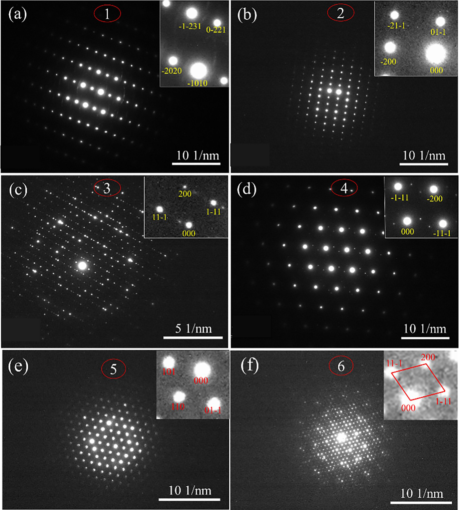
Figure 3 shows the TEM images of the IMCs on the Al/Mg bonding interface in conventional FSW. The IMC layer contains two sub-layers. According to the TEM-EDS line scan result (Figure 3(c)) and the electron diffraction pattern calibration (Figure 4(a–d)), it can be determined that the sub-layer close to the Al matrix is Al3Mg2, and the sub-layer near the Mg matrix is Al12Mg17. It is worth noting that the thickness of the IMC layer is not constant, the total thickness varies from about 1 µm (0.4 µm + 0.6 µm = 1 µm) to about 1.7 µm (0.6 µm + 1.1 µm = 1.7 µm). This is consistent with the results observed by scanning electron microscopy (SEM), that is, the thickness of the IMC layer changes even in the adjacent region [9]. At a location with thicker IMCs, the thickness of both sub-layers also gets bigger. However, the thickness of the Al3Mg2 sub-layer increases to a greater degree (from 0.6 to 1.1 µm). Some scholars pointed out that Al3Mg2 has lower activation energy than Al12Mg17, and thus has a faster growth rate [4, 13, 14], which is consistent with the experimental results in this study. It is necessary to point out that the temperature difference within such a short distance of a single micron is negligible. Therefore, the thickness variation of the IMC layer should be due to the difference in the atomic diffusion rate caused by the difference in the grain size or the local dislocation density of the materials on both sides.
(a) TEM image of IMC on the Al/Mg bonding interface in FSW, (b) the amplified TEM image of red rectangular in (a), (c) line scanning results along the blue dotted line in (a).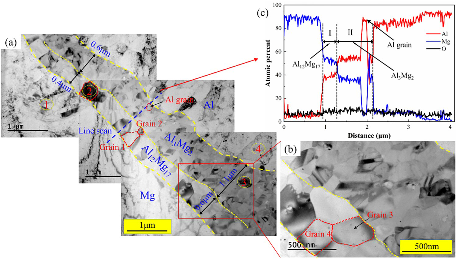
When the thickness of the Al12Mg17 sub-layer is small, this sub-layer has only one layer of grains, such as the grain marked circle 2 in Figure 3(a). But as its thickness increases, a second layer of grains appears, such as grain 1 and grain 2, in which grain 1 is the first layer of grains, and grain 2 is the second layer. When the Al12Mg17 sub-layer gets further thicker, the grain size of the second layer increases, such as grain 3 and grain 4, and the size of grain 4 in the first layer is almost the same as before. But the size of grain 3 in the second layer is significantly increased. This illustrates that the increase in the thickness of the Al12Mg17 sub-layer is achieved by the growth of a new grain layer.
For the Al3Mg2 sub-layer, since the grain boundary cannot be clearly characterised in the TEM image, it is difficult to determine whether the thickness increase is caused by the generation of a new grain layer or the increase in the original grain size. However, there is a more interesting phenomenon in the results of TEM-EDS, that is, an Al grain appears in the Al3Mg2 sub-layer. It should be noted here that because the grain boundary features are not clear enough, this red dashed line only shows the rough outline of the Al grain. During the Al–Mg isothermal diffusion treatment, individual Al grains would also appear in the Al3Mg2 sub-layer [14], so that it is impossible to determine whether an eutectic structure appears here. It is worth noting that the boundary of the IMC layer is relatively flat. As reported in the literatures [4, 15, 16], when the IMC layer was produced by solid-state diffusion reaction, the boundary of IMC layer is relatively flat, i.e. almost parallel to the local interface. Therefore, it was probably the atomic solid-state diffusion that resulted in the generation of IMC layer in this study.
Figure 5 shows the TEM image of IMCs on the Al/Mg bonding interface in UVeFSW. Like the case in conventional FSW, the IMC layer contains two sub-layers also in UVeFSW. And it can be determined by TEM-EDS (Figure 5(d)) and electron diffraction pattern calibration (Figure 4(e,f)) that the sub-layer near the Al matrix is Al3Mg2 (about 0.34 µm), while the sub-layer near the Mg matrix is Al12Mg17 (about 0.24 µm), and the thickness of the Al3Mg2 sub-layer was larger. In UVeFSW, the total thickness of the IMC layer does not change almost. However, because the observation area is limited, it can only show that the local thermo-mechanical condition is more uniform with the application of ultrasonic vibration. And the thickness of the whole IMC layer is significantly lower in UVeFSW than that in FSW, which is consistent with the results of the SEM images [9]. In addition, according to the slight contrast difference between different grains, the Al12Mg17 sub-layer contains only one layer of grain structure, such as grain 5 in Figure 5(c). As for the Al3Mg2 sub-layer, because the grain boundaries are not exhibited clearly, it is difficult to determine how many layers of grain structures are contained.
(a-c) TEM images of IMC on the Al/Mg bonding interface in UVeFSW, (d) line scanning results along the white dotted line in (a).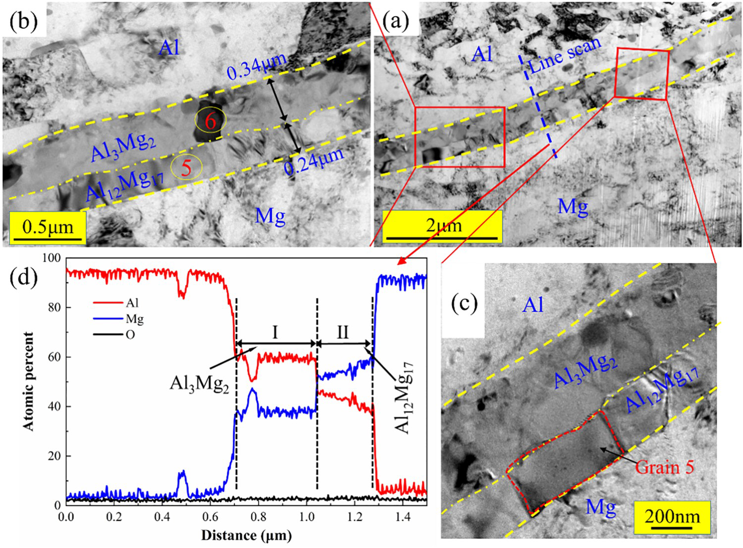
An interesting point is that in the EDS results cross the Al/Mg bonding interface in FSW (Figure 3(c)) and UVeFSW (Figure 5(d)), the composition change curve of the Al3Mg2 sub-layer is a plateau, while the Al12Mg17 has an obvious gradient, that is, the farther away from the Mg alloy side, the lower the Mg content. On one hand, this is due to atomic diffusion; on the other hand, according to the Al–Mg binary phase diagram, Al12Mg17 has a wider range of composition than the Al3Mg2 [17].
Measured temperature
Figure 6 shows the measured temperature in FSW and UVeFSW. For the temperature at the checking points 1 and 2 at the tool/workpiece interface, as shown in Figure 6(a,b), the temperatures near the shoulder bottom (point 1) and the pin side (point 2) fluctuate around 330°C and 360°C, respectively. There is almost no difference between FSW and UVeFSW. For the temperature outside the WNZ, as shown in Figure 6(c,d), the temperature in UVeFSW goes up earlier in FSW due to UV exerted in front of the tool. However, the difference in peak temperature is negligible (245.8°C in FSW and 244.5°C in UVeFSW). Thus, the exerted ultrasonic vibration has not caused temperature variation during the welding process, which is consistent with the observation results of Lv et al. and Hu et al. [3, 18].
The measured temperature (a) at tool/workpiece interface in FSW, (b) at tool/workpiece interface in UVeFSW, (c) thermal cycle outside the WNZ (AS), (d) the local amplified at peak value.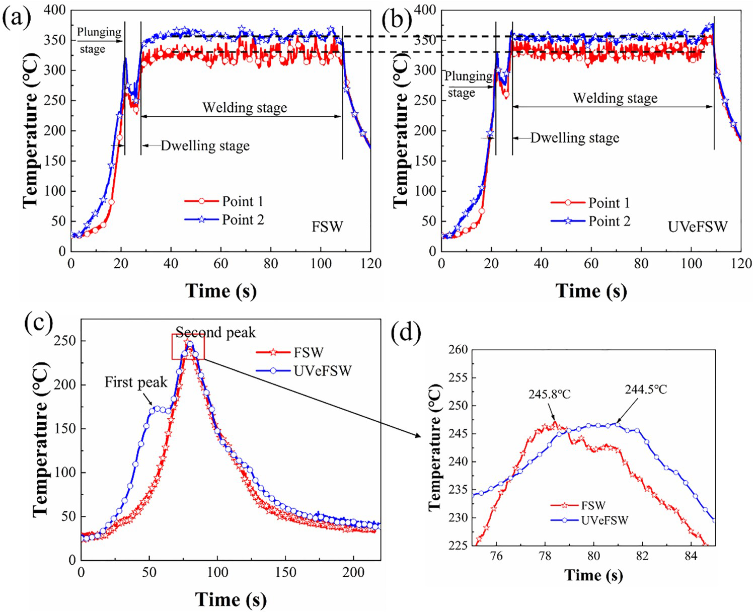
Regardless of conventional FSW and UVeFSW, the highest temperature did not reach the eutectic temperature points 450°C (L → Al3Mg2 + Al) and 437°C (L → Al12Mg17 + Mg). Moreover, according to the TEM characterisation, no eutectic structure is found, and the morphology of the IMC layer is more in line with the characteristics of the atomic diffusion reaction. Therefore, under the welding parameters used in this study, the formation mechanism of IMCs in FSW and UVeFSW is the atomic solid-state diffusion reaction.
EBSD characterization
Considering that the formation mechanism of IMC is a solid-state diffusion reaction in this study, and the evolution of grain structure on both sides of the IMC layer has an important influence on the atomic diffusion rate. Thereby, the grain structure on both sides of the IMC layer was characterised by EBSD.
Figure 7 shows the grain microstructure information in the Al alloy side near the IMC layer. The average grain sizes are 1.18 µm in FSW and 0.98 µm in UVeFSW, so that exerted UV slightly refined the grain size. Through observation, some recrystallized grains meet the characteristics of geometric dynamic recrystallization (GDRX), marked with black arrow; and some grains meet the characteristics of continuous dynamic recrystallization (CDRX) [19, 20], as shown with white dotted circle. But CDRX is the dominant mechanism. In addition, the degree of grain recrystallization is improved with the application of ultrasonic vibration (Figure 7(b,e)). That is, the area fraction of recrystallized grains, fRG, is 54.2% in FSW, while it increases to 66.8% in UVeFSW.
The IPF maps (a, d), grain morphology maps (b, e) and KAM maps (c, f) near IMC layer in Al side. (a, b, c): FSW; (d, e, f): UVeFSW.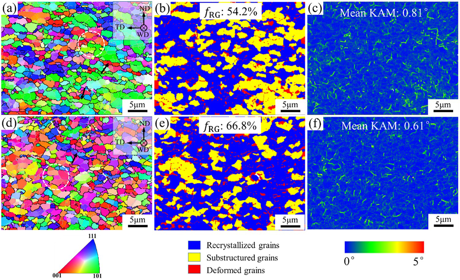
The microstructure information of the grains in the Mg alloy side near the IMC layer is shown in Figure 8. The average grain sizes are 2.57 µm in FSW and 2.32 µm in UVeFSW, which are much larger than those on the Al alloy side because Mg alloy and Al alloy have different stacking fault energy and initial grain size. The recrystallization grains here meet the characteristics of discontinuous dynamic recrystallization-DDRX (as shown with black arrow) and CDRX (as shown with white dotted circle) [20, 21]. And CDRX is the dominant mechanism. With applied ultrasonic vibration, the degree of recrystallization is also improved like the Al side.
The IPF maps (a, d), grain morphology maps (b, e) and KAM maps (c, f) near IMC layer in Mg side. (a, b, c): FSW; (d, e, f): UVeFSW.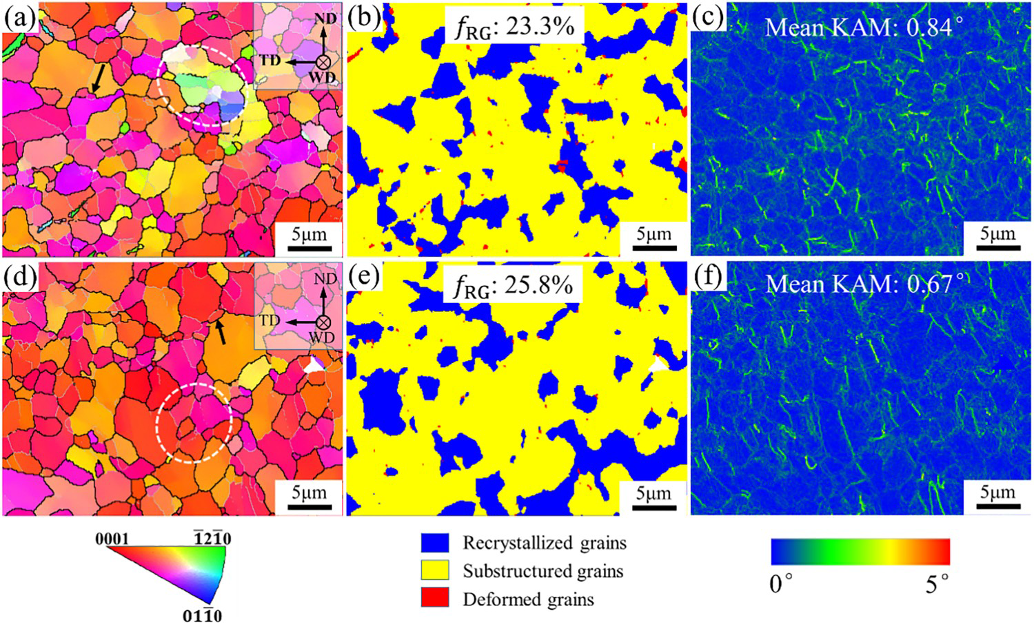
The reason why the applied ultrasonic vibration increases the recrystallization degree of grains may be explained as follows. The recrystallization process of grains, especially CDRX, involves dislocation movement, and ultrasonic vibration can promote dislocation movement [22, 23], thus accelerating the transition from low-angle grain boundary (LAGBs) to high-angle grain boundary (HAGBs) [24]. Therefore, ultrasonic vibration can improve the recrystallization degree of grains. In this process, dislocations are also consumed in large quantities, so that the KAM value in the observation area decreases in UVeFSW. The KAM value can be used to indicate the uniformity of material deformation and dislocation density. The smaller the KAM value, the lower the dislocation density [25, 26].
Why UV inhibiting the growth of IMCs
From this study and previous research results [3, 9, 10], we can know that ultrasonic vibration can significantly inhibit the growth of IMC layer. How did ultrasonic vibration do this? According to the aforementioned analysis, it can be determined that under the welding parameters (800 rev min−1 – 50 mm min−1) used in this research, the IMC layer on the Al/Mg bonding interface is generated by atomic solid-state diffusion reaction. Therefore, this issue can be discussed in terms of the factors affecting atomic diffusion, such as temperature, composition, crystal structure and short-circuit diffusion.
First of all, the temperature variation curve inside and outside the WNZ (Figure 6) has proved that the ultrasonic vibration does not affect the welding temperature. Second, the Al matrix and Mg matrix on both sides of the IMC layer are the same in FSW and UVeFSW, and there is no difference in composition and crystal structure. Finally, short-circuit diffusion mainly refers to the diffusion of atoms through defects such as the grain surface, grain boundaries, and dislocations. From the grain microstructure in FSW and UVeFSW, the difference in grain sizes is too small to have a noteworthy effect on atom diffusion. Therefore, the difference between lattice diffusion, boundary diffusion and surface diffusion in the high-temperature environment of conventional FSW is negligible. However, quantities of dislocations produced in the welding process can significantly facilitated diffusion rate due to the smaller diffusion activation energy. And ultrasonic vibration has a significant effect on dislocation motion. Thus, dislocation density should be the key factor to affect the atomic diffusion rate.
Ultrasonic vibration accelerates the generation of HAGBs by promoting the movement, rearrangement and aggregation of dislocations, and it also consumes more dislocations [22-24]. At the same time, it can also improve dipole annihilation. Therefore, the dislocation density decreases when ultrasonic vibration is applied. By comparing the KAM images in Figures 7 and 8, it is found that ultrasonic vibration does reduce the dislocation density around the IMC layer. Because the dislocation density as the diffusion channel decreases, the diffusion rate of Al/Mg atoms gets lower, and the growth of IMC naturally is suppressed. It is worth noting that this explanation is still based on speculation to some extent because the interaction of ultrasonic vibration with the thermo-mechanical process in FSW and its effect on IMC growth are very complicated. It needs further investigation in the next step.
Conclusions
Under the welding conditions in this study, the IMC layer formed at Al/Mg interface contained two sub-layers of Al3Mg2 and Al12Mg17, but the IMCs thickness was significantly reduced when the ultrasonic vibration was applied. The measured temperature at the tool/workpiece interface was far below the eutectic points in both FSW and UVeFSW so that the IMCs were generated by solid-state atomic diffusion in butt joining of dissimilar Al/Mg alloys. The EBSD characterisation showed that ultrasonic vibration improved the degree of gains recrystallization on both sides of the IMC layer by promoting the movement and consumption of dislocations. It may be speculated that the decreasing dislocation density reduced the diffusion rate of atoms so that the growth of IMC layer was suppressed.
Footnotes
Disclosure statement
No potential conflict of interest was reported by the author(s).