
Abstract
Sn–Sb solder alloys (2; 5.5 and 10wt-% Sb) were directionally solidified with a view to permitting the effect of a wide range of solidification cooling rates to be related to the resulting microstructure, which is shown to be formed by a cellular Sn-rich matrix with Sn–Sb intermetallic particles (IMCs) randomly distributed in the matrix The corrosion resistance of these alloys is investigated by electrochemical impedance spectroscopy (EIS), equivalent circuit and linear polarisation and the results correlated with microstructural features. The increase in the alloy Sb content is shown to change the nature/morphology of the Sn–Sb IMCs, consequently affecting the corrosion resistance. The EIS data indicated that the Sn–10wt-%Sb alloy has the best corrosion resistance because of the high resistance of its oxide barrier layer. The polarisation curves also indicate lowest corrosion rate and nobler potential related to the Sn–10wt-%Sb alloy, which has also been confirmed by calculations of polarisation resistance.
Introduction
Sn–Pb solder alloys have been widely applied in the electronics industry, particularly for manufacturing components and units of communication and navigation systems. However, due to recent legal restrictions for Pb-based solders, Pb tends to be banned from industrial parts due to its harmful effects on human health and to the increasing environmental concerns over its toxicity. In recent years, the legislation has become even more restrictive, which has significantly increased the research and development of lead-free solder alloys [1–4]. Not only good electrical and thermal performances are required of a solder alloy but also mechanical and electrochemical reliability [5,6]. With this goal, alternative alloying elements have been examined as replacements for Pb on Sn-based alloys, such as Ag, Cu, Zn, In, composing alternative alloys systems, such as Sn–Ag–Cu, Sn–Zn–Ag, Sn–Zn–In, Sn–Zn–Ag–Al, Sn–Ag–Bi–Cu, Sn–In–Ag–Sb [5–8].
Unusual microstructural arrays can be formed during soldering, which are associated with the high cooling rates of soldering processes. Studies on Sn-based alloys report that the solidification conditions affect not only the morphology but also the microstructure length-scale of the β-Sn phase, which governs the solder mechanical properties due to its interaction with intermetallic compounds (IMCs) that are formed in the as-soldered Sn-rich joints [9–12]. It is well known that the resulting microstructure also significantly affects the corrosion behaviour of solders, as reported in some studies on corrosion behaviour of lead-free solders in corrosive solutions such as NaCl and acid solutions [1,2,13–16]. Sn–Sb alloys are some of the most promising candidates for the replacement of Pb–Sn solders due to their compatible tensile properties and wettability, as recently reported by Dias and co-authors [17,18]. Despite the good creep resistance of the Sn–5wt-%Sb alloy and its suitability for high temperature applications (melting range 232-240°C), Sb has restrictions as an alloying element due to its toxicity, however, it is considered of medium risk in Europe while Pb is considered of high risk [19,20]. These authors investigated both hypoperitectic [17] and peritectic [18] Sn–Sb alloys, which have microstructures formed by a cellular β-Sn matrix for the range of cooling rates typically used in solders, with Sn–Sb intermetallic particles (IMCs) distributed throughout the matrix. Contradictions exist in the literature with respect to the composition of the IMC in the microstructure of the Sn–Sb alloys, that is, either SnSb [17] or Sn3Sb2 [21] have been reported to occur. Although a series of studies concerning phase equilibria in Sb–Sn system have been performed, there is not a consensus regarding the definition of the solid-state phases [22]. The tensile strength was shown to increase with the decrease in the length scale of the cellular microstructure for a hypoperitectic Sn–5.5wt-%Sb alloy, whereas for a hyperperitectic Sn–10wt-%Sb alloy the tensile strength remained unaffected with the evolution of the cellular spacing [18]. Such different behaviour has been attributed to the different IMCs that were reported to occur, i.e. SnSb and Sn3Sb2, respectively, and to the higher volume fraction of the latter IMC in the microstructure of the hyperperitectic alloy. However, to the best of the present author's knowledge, studies on the effect of such microstructural features of Sn–Sb alloys on the electrochemical corrosion response cannot be found in the literature.
This work focuses on the experimental evaluation of the electrochemical impedance behaviour of Sn–Sb solder alloys (2, 5.5 and 10wt-% Sb), which were previously subjected to directional solidification with a view to permitting the effect of a wide range of solidification cooling rates to be examined in the resulting microstructures. High cooling rates, typical of soldering processes, are associated with the refinement and distribution of the phases forming the alloy microstructure, which according to reports in the literature can have a direct influence on the corrosion behaviour of solder alloys [1 3]. This work aims to explore the roles played by the alloy Sb content as well as by the type and distribution of IMCs in the alloy's microstructure on the subsequent corrosion resistance.
Experimental procedure
Solder alloys, solidification system and microstructural characterisation
Commercially pure Sn (containing 0.0469 wt-% Pb, 0.0081 wt-% Fe, 0.0005 wt-% Sb, 0.00001 wt-% Cd, 0.0001 wt-% Ni, 0.0047 wt-% Cu, 0.0046 wt-% Bi and 0.0001 wt-% Zn) and commercially pure Sb (containing 0.215 wt-% Pb, 0.075 wt-% Fe, 0.034 wt-% Ni, 0.034 wt-% Cu and 0.009 wt-% Si) were used to prepare the Sn–2wt-%Sn, Sn–5.5wt-%Sn, Sn–10wt-%Sn alloys.
With a view to promoting solidification cooling rates of the same order of those typical of soldering processes, samples of Sn–Sb alloys having 2, 5.5 and 10 wt-%Sb were directionally solidified (DS) by using a water-cooled solidification setup, which promotes solidification under transient heat flow regime. Details on the experimental procedures regarding the solidification experiments can be found in previous works performed on Sn–Sb alloys [17,18]. The corresponding partial Sn–Sb phase diagram (Figure 1), adapted from Okamoto [21], include the selected alloys compositions to be studied in this work.
Partial Sn–Sb phase diagram (adapted from Okamoto [21]) highlighting the alloys compositions examined in the present study.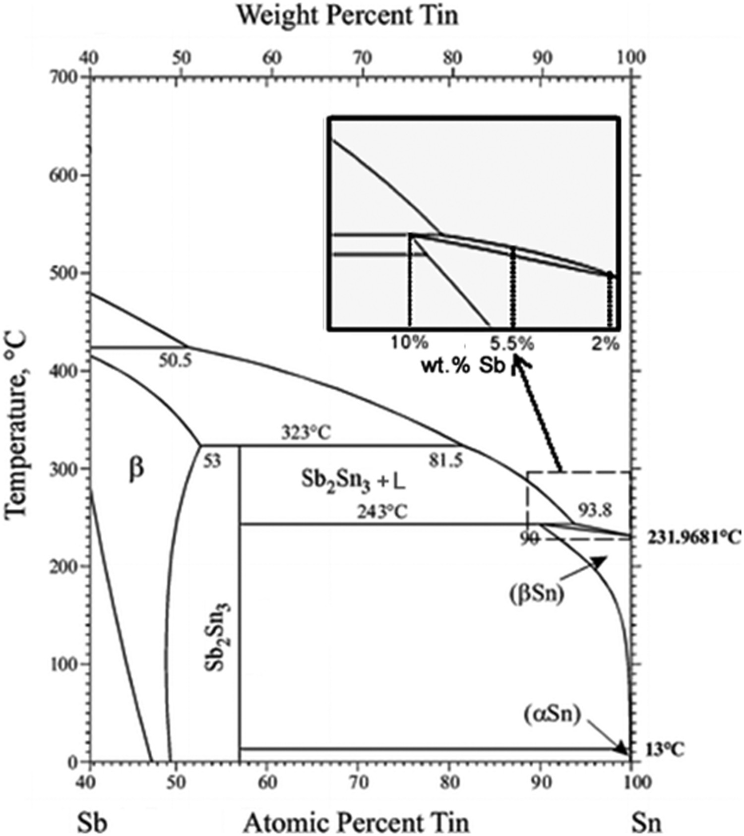
The metallographic procedure consisted on polishing the samples with 100-1200 grit SiC papers, followed by final polishing with diamond paste (1-3μm). To reveal the microstructure, a solution of 2 ml hydrochloric acid (HCl), 3 mL nitric acid (HNO3), and ethyl alcohol to achieve 100 mL was used.
An Olympus Inverted Metallurgical Optical Microscope (model 41GX) was used to examine the alloys microstructures. The cellular spacing of the β-Sn matrix (λ c) was measured from the optical images of the samples by the triangle method [23]. With a view to parameterising the length scale of cellular microstructure, thus permitting the effect of the increasing alloy Sb content on the corrosion behaviour to be examined, one sample of each DS alloy casting having similar λ c values were taken for the experimental corrosion analysis (P1 = Sn–2wt-%Sn, P2 = Sn–5.5wt-%Sn and P3 = Sn–10wt-%Sn alloys).
To permit a complete mapping of the microstructural phases to be obtained, the alloys samples were also examined by a scanning electron microscope FEI Quanta 650 – FEG and the crystalline phases were characterised in an Advance D8, Bruker, X-ray diffractometer (XRD) of the Brazilian Nanotechnology National Laboratory- LNNano, with 2θ range of 25°–70°, step of 0.04°, under rotation mode and Cu-Kα radiation (λ = 0.15406 nm). Additionally, the measurements were performed using a peak integration method, where multiple scans were performed in a certain long period of time, (in this case, for 4 h) and the obtained data are were integrated, thus ensuring high resolution of the peaks and high data rates.
Electrochemical measurements
For the accomplishment of the electrochemical tests, a three-electrode system model was used, where the Ag/AgCl is the reference electrode, the platinum wire is a counter electrode and the Sn–Sb alloy samples were used as the working electrodes (WE). The WE of the Sn–Sb alloy samples (Sn–2wt-%Sn, Sn–5.5wt-%Sn, Sn–10wt-%Sn alloys), previously ground up to a 2000 grit SiC finish, were positioned at the electrochemical cell leaving a circular area of 0.5 (±0.02) cm2 of the sample surface exposed and in contact with 20 mL of a 0.07 M NaCl solution at room temperature (25°C). The use of such dilute NaCl solution (0.07 M) is justified since higher concentrations, such as the standard 0.5 M, were shown to be too aggressive, hindering the microstructure response to the solution. That is, a trend in the corrosion resistance can be assessed by using an about 10 times diluted NaCl solution. The electrochemical impedance spectroscopy and linear polarisation tests were performed in triplicate using a potentiostat/galvanostat Autolab® model PGSTAT-128N.
Electrochemical impedance spectroscopy (EIS) measurements were carried out after 15 min of immersion in the electrolyte at room temperature (25°C). A potential signal amplitude of 10 mV (SCE) was applied, as well as 10 points per decade in a frequency range of 105 to 10−2 Hz. The EIS results and parameters were quantified using the ZView® software. Fitted and experimental data were compared, and the quality of the fit has been evaluated by chi-squared (χ 2) parameters for each examined Sn–Sb alloy sample. The polarisation tests were carried out after the EIS tests at a scan rate of 0.167 mV/s from −0.75 to −0.10 V. vs. open-circuit potential (OCP). The corrosion current densities (i corr) were estimated from the potentiodynamic polarisation curves, by Tafel's extrapolation, using both cathodic and anodic branches.
Results and discussion
Cooling rate and microstructure
The directional solidification process, under a transient regime of heat extraction, results in a range of solidification cooling rates (Ṫ) along the length of the DS castings. The Sn–Sb alloys (2.0, 5.5, and 10 wt-% Sb) examined in the present study have a β-Sn matrix characterised by a cellular morphology. In Figure 2, the evolution of the cellular spacing, λ c, (mean values and error bars representing the range of maximum and minimum experimental measurements) is correlated with the experimental Ṫ values for the DS Sn–Sb alloys castings, where typical cross-section microstructures of the Sn–Sb alloys casting of samples having a similar cellular spacing (of about 20 µm) can be observed. The average values of λ c are 19.7, 20.3 and 19.9 µm for the Sn–2wt-%Sb (P1), Sn–5.5wt-%Sb (P2) and Sn–10wt-%Sb (P3) alloys samples, respectively, which were selected to permit the cell spacing around 20 µm to be parameterised. As a matter of soldering applicability, the parameterisation also has taken into account the cooling rate values typical of reflow procedures in industrial practice, which comprehend the range at about 3.0-10.0 K/s [24]. It is known that the magnitude of the length scale of the alloy matrix can influence the corrosion behaviour of solder alloys [1 3]. The parametrisation of such microstructural feature will allow the analysis to be focused on the influence of the increasing alloy Sb content on the corrosion behaviour.
Cellular spacing (λ c) as a function of cooling rate (Ṫ) for the Sn–Sb alloys, and the microstructures of samples selected for corrosion analysis.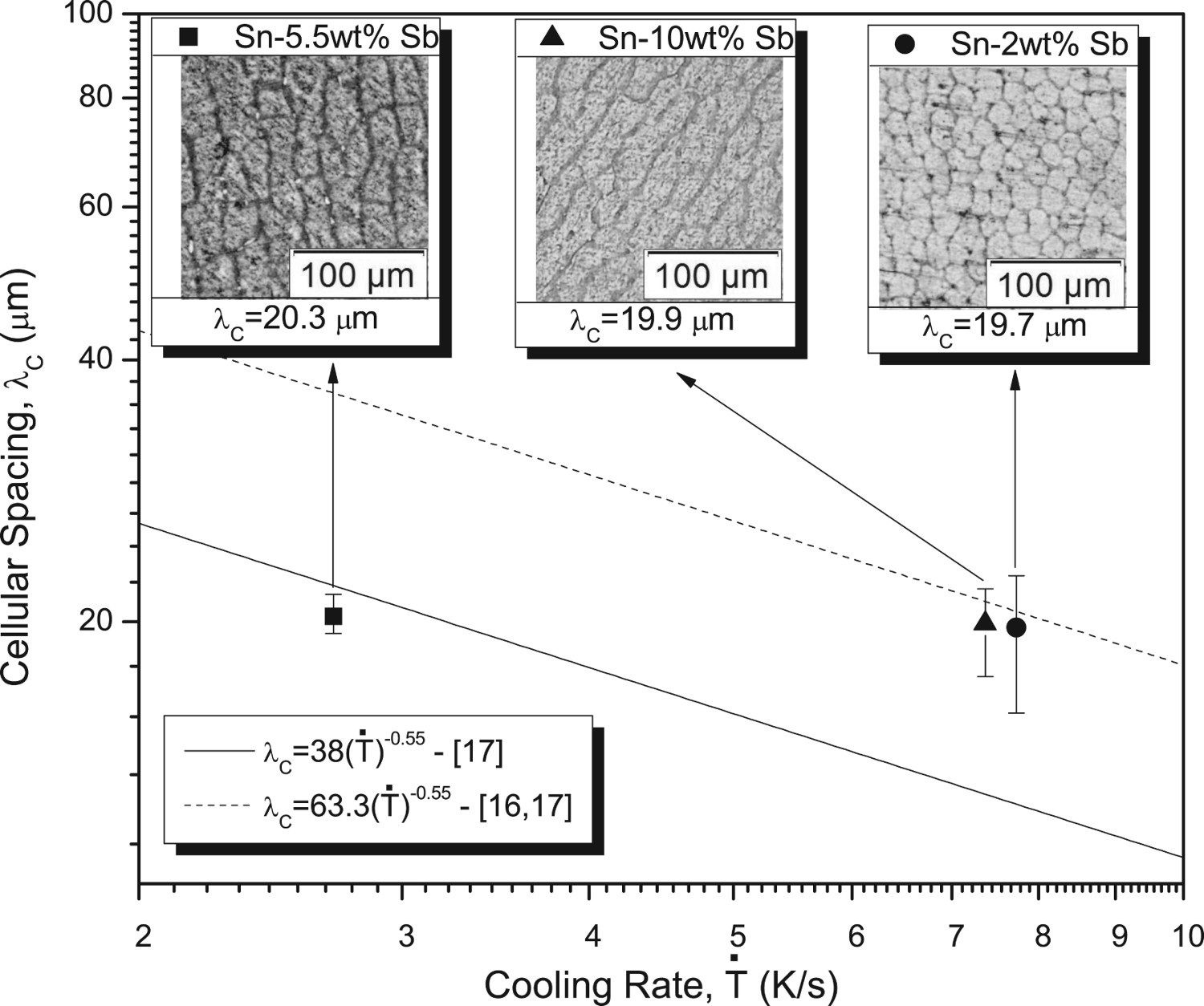
The phases forming the microstructures of the Sn–Sb alloys were characterised by X-ray diffraction with Cu-Kα radiation. The resulting XRD patterns (Figure 3), show that the Sn(β) and the SnSb phases constitute the microstructural phases of both the Sn–2wt-%Sb and Sn–5.5wt-%Sb alloys samples, whereas the Sn(β), SnSb and the Sn3Sb2 phases form the microstructure of Sn–10wt-%Sb alloy sample. These XRD patterns were associated with a crystallographic database – the Inorganic Crystal Structure Database–ICSD [25]. In a previous study [17], which confirmed the occurrence of such IMCs despite the contradictions existing in the literature with respect to their compositions. In the present investigation, more detailed diffractogram data were obtained using a detector with higher resolution than that of reference [17], which has been employed with the aim to identifying the presence of the IMCs previously reported in the literature. Figure 3 shows peaks related to the XRD data of α-Sn and β-Sn phases, reported with a cubic and tetragonal crystal structure, respectively. The α-Sn phase shows a Fd-3 ms space group and lattice parameters a = b = c = 6.489 Å [26], while the β-Sn phase shows a I 41 / a m d s space group and lattice parameters a = b = 5.831 Å, and c = 3.182 Å [27]. The β-Sn or (Sn)rt phase is formed by a peritectic reaction described as: L + Sn3Sb2 ↔ (Sn)rt at 243°C giving rise to the (Sn)lt phase or the so-called α-Sn phase through the (Sn)rt ↔ (Sn)lt reaction at 13°C [28]. Although considerable intensity peaks associated with the α-Sn phase in Figure 3(a–c), they are insufficient to assign this phase since only a single peak was detected for each alloy sample. In addition, the samples have not undergone temperatures below 13°C and it is reported that the addition of antimony suppress the (Sn)rt ↔ (Sn)lt transformation [29].
X-ray diffraction (XRD) patterns of: (a) P1 = Sn–2wt-%Sb, (b) P2 = Sn–5.5wt-%Sb and (c) P3 = Sn–10wt-%Sb alloy samples.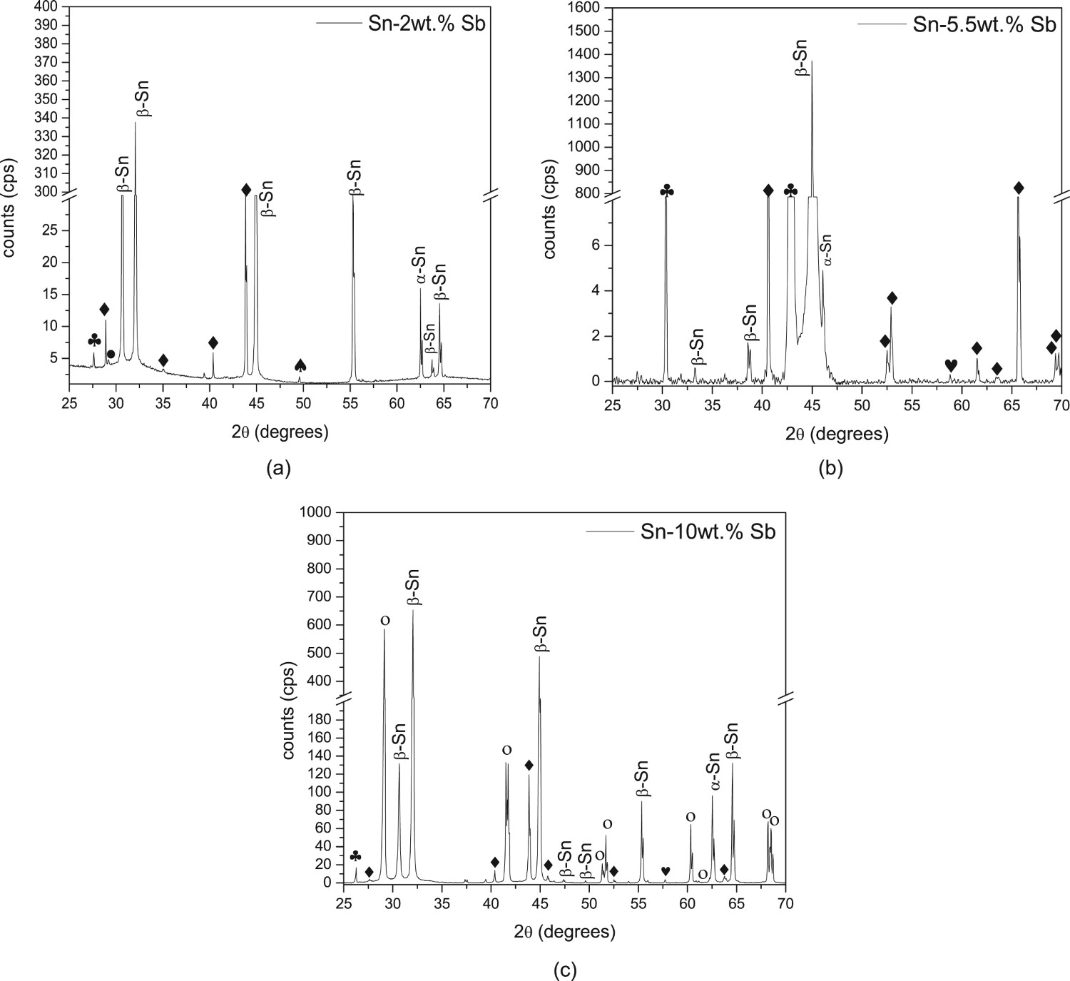
The SnSb IMC was shown to be divided into five different crystal structures. The first three SnSb IMCs identified have cubic systems, which are represented below ♣, ♥ and ♠, with F m / 3 m space group and lattice parameters a = b = c = 5.880 Å [30]; a P m / 3 m space group and lattice parameters a = b = c = 3.550 Å [31], and a F – 4 3 m space group and lattice parameters a = b = c = 6.142 Å [32], respectively. Also, it was possible to identify the SnSb IMC with trigonal system with R – 3 m H space group, but with two lattice parameters identified represented bellow as, with: a = b = 4.326 Å and c = 5.346 Å [33] and ♦ with a = b = c = 6.226 Å [34]. Among the analysed peaks, the more frequent one is ♦, while the remaining ones appeared one or two times in the diffractograms (Figure 6(a–c)). The Sb2Sn3 IMC was identified as
The microstructure of the examined Sn–Sb alloys was shown to be formed by β-Sn of cellular morphology (Figure 2) having Sn–Sb intermetallic particles randomly distributed into the β-matrix. The morphologies of these IMCs in the microstructure were identified using high-resolution SEM analyses. In the case of the hypoperitectic alloy (5.5 wt-%Sb) the IMCs appear as SnSb nano-precipitates (Figure 4(b)), whereas for the hyperperitectic alloy (10wt-%Sb) as Sn3Sb2 precipitates having a faceted shape, as shown in Figure 4(c). Despite the use of larger SEM magnification on the 2wt-% Sb and 10wt-% Sb alloy samples, the SnSb particles could not be visualised (Figure 4(a,c)). It is worth noting that the cellular spacing has been parameterised at about 20 μm in the examined alloys samples in order to highlight the microstructural differences in terms of IMCs due to the alloy Sb content and solidification cooling rate. Thus, it seems that for the two examined hypoperitectic alloys, the SnSb IMC grows preferentially for the case of the Sn–5.5wt-%Sb alloy due to the lower solidification cooling rates (Figure 2) and to the higher alloy Sb content. For the hyperperitectic alloy, Sn–10wt-%Sb, the Sb content beyond the peritectic concentration and the higher cooling rate seem to induce the growth of the Sn3Sb2 IMC.
SEM images of typical morphologies and distribution of IMCs: (a) no SnSb particles visualised: Sn–2wt-% Sb alloy; (b) SnSb nanoparticles: Sn–5.5wt-%Sb alloy and (c) Sn3Sb2 particles having faceted shape: Sn–10wt-%Sb alloy.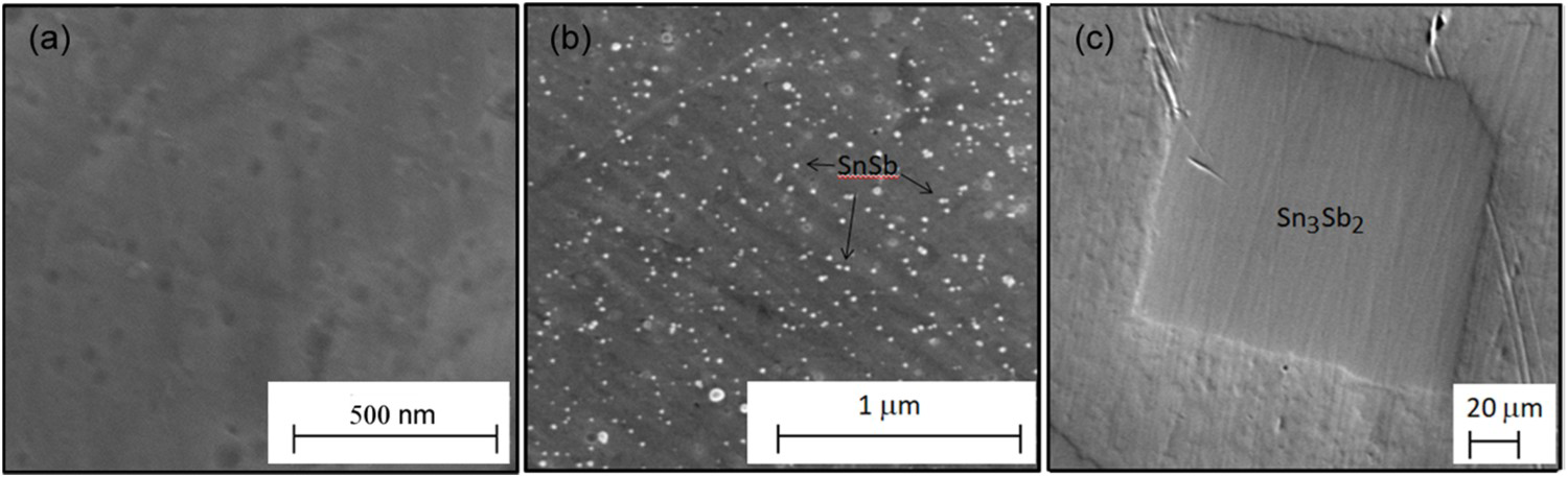
EIS measurements and equivalent circuit
The EIS analyses were performed in a naturally stagnant 0.07 M NaCl solution at room temperature (25°C). Figure 5 shows the simulated Bode diagram and Nyquist plots for the three analysed samples. Investigations on Sn alloys reported the use of a one-time constant circuit for frequencies in the range of 105–10−1 Hz [1,2,36 38]. For low frequencies (105–10−2Hz), a few studies have been carried out in which two-time constants equivalent circuits are proposed [39,40]. To the best knowledge of the present authors, no study has been reported investigating the corrosion mechanism of Sn–Sb alloys. The present study contributes to a systematic analysis of Sn–Sb alloys at low frequencies (105–10−2 Hz) and propose a comparison between one-time constant R sol(R (1)(CPE(1)) and two-time constants R sol(R (2)(CPE(2)(CPE(1)R (1)))). The low-frequency study is necessary due to the high stability of the Sn–Sb alloys until 10−1 Hz, showing the same behaviour of studies reported for Sn-based alloys [1,2,36 38]. It is worth noting that is possible to observe in the 10−1–10−2 Hz range, a slight change in the behaviour of the Sn–Sb alloys which is associated with a second time constant.
Experimental data for the Sn–Sb alloys samples: (a) Bode diagram, (b) Nyquist plot for one-time equivalent circuit, (c) Nyquist plot for two-time equivalent circuit and, (d) the imaginary part of the impedance as a function of frequency.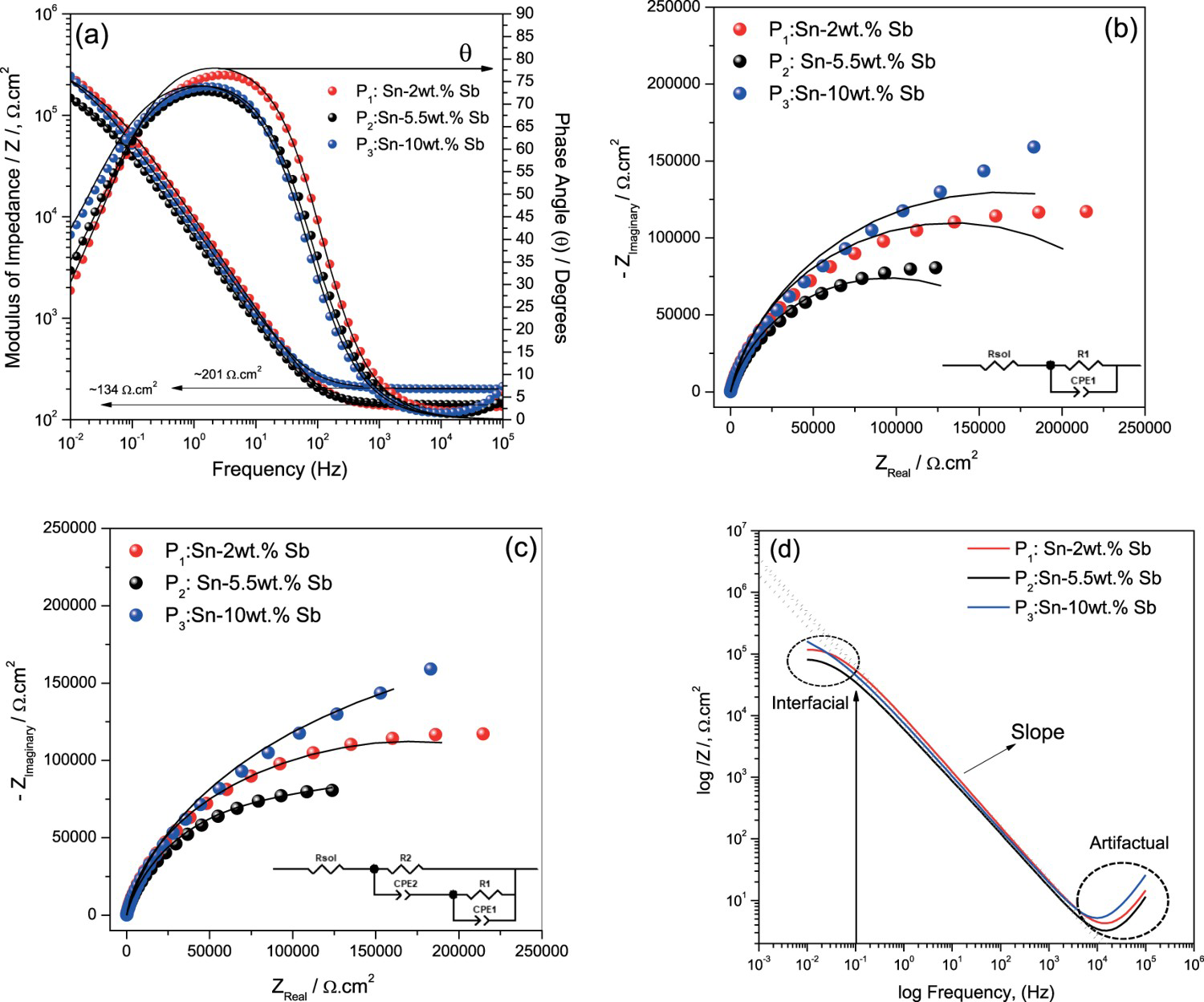
Analysing the Bode diagram in Figure 5(a), it is possible to conclude that they provide the maximum modulus of impedance (|Z|) at low frequencies, from which, it can be obtained the resistance of solution (R sol) at a high frequency range of 104–105 Hz, with very similar |Z| values of about 134 Ω cm2 for P1 and P2 and 201 Ω cm2 for P3. At low frequencies, it is possible to obtain the data related to the charge transfer resistance (R 1), and also, it is noted that the sample with the lowest modulus of impedance is P2 (5.5wt-% Sb), which indicates a greater corrosion susceptibility when compared to P1 and P3. Graphically, these values are in a frequency range of 10−1–10−2 Hz which suggest the occurrence of a reaction between the electrolyte and the sample. In Bode diagrams, similar maximum phase angles (θ max) can be observed for all the examined samples, that is of about 76° for P1 and 74° for P2 and P3.
Figure 5(b,c) shows the Nyquist plots with the fitted data for one-time and two-time constants circuits, respectively. The plots show three different capacitive semi-arcs and differently from the Bode diagrams, the diameter of the capacitive semi-arcs clearly increased, with the P2 sample presenting the smaller capacitive arc and the P3 sample the highest capacitive arc. These results point out to a higher susceptibility to corrosion associated with the P2 sample and a greater tendency of corrosion resistance associated with P3. Once the highest corrosion resistance obtained in polarisation and EIS tests are associated with the highest capacitive arc [41,42], it is possible to say that is the case of P3. It is worth noting that when observing the fitted results (black lines) in Figure 5(b), the equivalent circuit with one-time constant does not address the low frequencies, disregarding the part that differentiates the corrosion behaviour among the Sn–Sb alloys. In other words, excluding frequencies below 10−1 Hz would show that all the three alloys have practically the same corrosion behaviour, which is exactly the core contribution of the present work.
Figure 5(d) shows the imaginary part of the impedance as a function of frequency where the artefactual behaviour is characterised by 105–104 Hz and can be attributed to the solution resistance (R sol), the slope is associated with the reactions related to the sample (R (1)(CPE(1))) at 104–10−1 Hz and the interfacial reaction occurs at 10−1–10−2 Hz and it is represented by (R (2)(CPE(2))).
The aforementioned analysis of Figure 5 permits to conclude that the electrochemical corrosion resistance may be related to the IMCs present in the β-Sn matrix, since the P3 sample is the only examined sample having SnSb and Sn3Sb2 IMCs in its microstructure, the latter being clearly observed in the SEM image of Figure 4(c). On the other hand, P1 presents the SnSb particles well distributed in the β-Sn matrix, which have been successfully identified through XRD analyses, because these particles are present in the matrix in nanoscale size and they could not be well visualised in SEM images. The P2 sample has also the SnSb IMC in nanoscale size disseminated throughout the β-Sn matrix, but its particle size can be observed from SEM images, as shown in Figure 4(b). Besides, the P2 sample shows higher concentration of SnSb IMC as compared to the P1 sample, factor that can indicated a lower corrosion resistance associated with P2, despite its higher nominal Sb composition as compared to P1. In contrast, the P3 sample, which has the highest Sb content, shows the same SnSb peaks as the P1 sample, with an additional one related to the Sn3Sb2 IMC and shows the best tendency to corrosion resistance among all samples.
Equivalent circuit analyses
In order to quantify the impedance parameters, thus permitting a more consistent correlation with the alloy microstructure to be done, two models of equivalent circuit have been proposed, as follows. The two proposed equivalent circuit features resistance and CPE elements for one and two-time constants. The impedance value of the constant phase element (Z CPE) is calculated by the expression: Z CPE = (1/[T.(jω)
n
]), where T represents frequency, independent data obtained by the Z-View software; j is an imaginary number; ω is the angular frequency, which is calculated by 2πf, where f is the frequency; n is a dimensionless value between 0 and 1 [43 48]. The n element demonstrates whether CPE is ideal, that is when n = 1; when n presents lower values, it means that there is an interference of the surface; n = 0.5 means the Warburg element; and n = 0 demonstrates that the CPE becomes a resistor [49]. Figure 6(a) shows one-time constant equivalent circuit and Figure 6(b) shows the proposed model for two-time constants equivalent circuit.
Proposed equivalent circuits for modelling impedance parameters for Sn–Sb alloys samples in a 0.07 M NaCl solution at 25°C.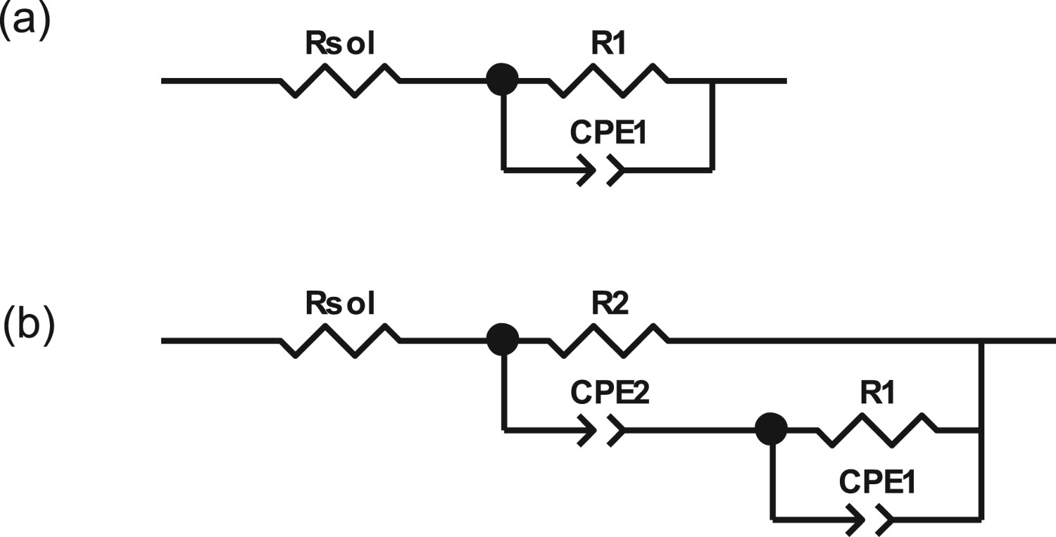
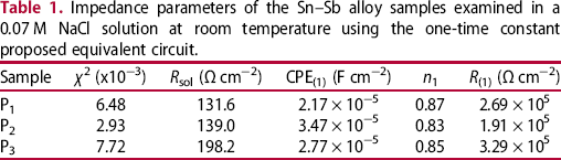
Impedance parameters of the Sn–Sb alloy samples examined in a 0.07 M NaCl solution at room temperature using the one-time constant proposed equivalent circuit.
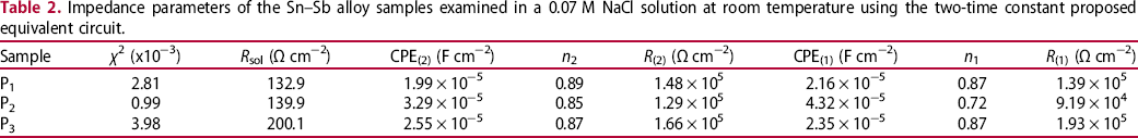
Impedance parameters of the Sn–Sb alloy samples examined in a 0.07 M NaCl solution at room temperature using the two-time constant proposed equivalent circuit.
In Figure 5(b), it is possible to observe the fitted equivalent circuit for one-time constant (R sol(R (1)(CPE(1)))), which is compatible only up to a frequency of about 105–10−1 Hz range. In contrast, for a frequency range of 10−1–10−2 Hz, i.e. low frequencies, the simulated results are not consistent with those obtained experimentally. Consequently, the three analysed samples may have different behaviour at low frequencies, indicating the formation of an oxide layer characterising the interface oxide||electrolyte. In the (R sol(R (1)(CPE(1)))) circuit, the R (1) corresponds to charge transfer processes through the thin oxide film on the alloy surface and CPE(1) is associated with a oxide layer capacitance.
Looking closely at Figure 5(a) (Bode diagram) at low frequency ranges and the number of time constants (Figure 5(d)) can be identified when the modulus of the imaginary part of the impedance vs. frequency of the alloy samples examined are plotted in logarithmic representation. The 104–105 frequency range is attributed to a solution resistance effect and was deleted from the CNLS analysis since it has been attributed to artefactual effects. At the Bode diagram, a first-time constant is clearly occurring between 104–10−1 Hz and another between 10−1–10−2 Hz. Thus, it is necessary to analyse the obtained data using a two-time constants circuit, which it is appropriate to understand the actual behaviour of the alloy samples at low frequencies. For this purpose, the (R sol(R (2)(CPE(2)(CPE(1)R (1))))) circuit was chosen, where the CPE(1)/R (1) couple corresponds to the metal||oxide interface and the second CPE(2)/R (2) couple is attributed to the oxide||electrolyte interface.
The P2 sample shows the highest values for R (1) and CPE(1) for the metal||oxide interface as compared to the other samples (9.19 × 10⁴ Ω cm–2 and 4.32 × 10⁻⁵ F cm–2, respectively) indicating a higher tendency to corrosion. The values R (1)/CPE(1) attributed to the P3 sample indicate higher corrosion resistance (1.93 × 10⁵ Ω cm–2 and 2.35 × 10⁻⁵ F cm–2, respectively) as compared to P1 and P2 samples, while the P1 sample stands with intermediate values (R (1) = 1.39 × 10⁵ Ω cm−2 and CPE(1) = 2.16 × 10⁻⁵ F cm−2).
The oxide||electrolyte interface, which corresponds to the CPE(2)/R (2) couple was also analysed. When the results obtained for the P3 sample are compared to those of P1 and P2, it can be observed that the thin film oxide layer formed on the metal surface indicates lower corrosion resistance (R (2)) since these parameters are related to the corrosion product formed on the surface of the material. The capacitance values (CPE(2)) show a reduction in the obtained values of about 1.6 times considering P2/P1 samples and a reduction of 1.3 times for P2/P3 samples. Considering that R 2 increased about 1.3 times from P2 to P3, and 1.1 times from P1 to P3, it is possible to conclude that P3 shows greater protection against corrosion as compared to P1 and P2. Considering such factors, it is possible to synthesise the sequence of corrosion resistances of all examined samples as P3 > P1 > P2.
Potentiodynamic polarisation plots
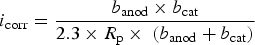
Figure 7 shows the potentiodynamic polarisation curves obtained from +0.450 to –0.250 V vs EOCP (Ag/AgCl) for pure Sn and P1, P2 and P3 samples. Sn–Sb alloys samples were selected with the approximated average values of cell spacings (λ c) of 19.7, 20.3 and 19.9 µm, respectively. Tafel extrapolation was used to obtain the experimental corrosion current density (i corr) using both cathodic and anodic branches of the polarisation curves along a range of potentials. Parameters and observation of these results reinforce the corrosion resistance tendency observed previously with the EIS fitted results, i.e. better electrochemical corrosion resistance being associated with the P3 sample. These results can be better observed in Table 3.
Experimental potentiodynamic curves for (a) pure Sn samples and, (b) Sn–Sb alloy samples. Summarised polarisation parameters of the Pure Sn and Sn–Sb alloy samples examined in a 0.07 M NaCl solution at room temperature.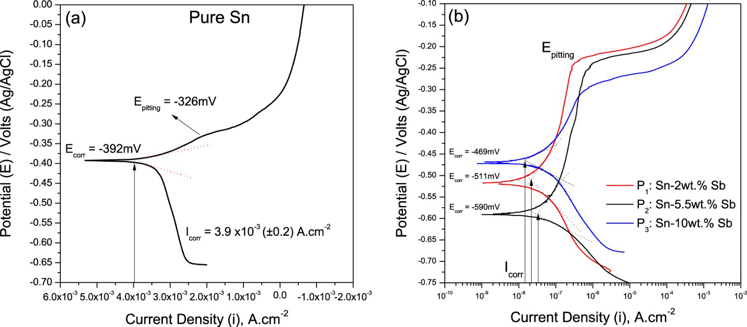
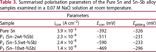
The E corr values obtained for each sample show differences in the corrosion potential between P3 and P1 samples and P1 and P2 samples, of 42 and 79 mV, respectively. Considering a microstructural evaluation, such values indicate that the resulting potentials (E corr) are directly affected by the Sb content of the examined Sn–Sb alloys. The sample of the alloy of highest Sb content had the corrosion potential shifted towards the nobler side. The highest potential is that of P3, followed by the P1 sample, and finally by the P2 sample. The polarisation curves indicate that the P3 sample shows the lowest i corr (1.4 × 10⁻⁸ A cm−2) as compared to P1 (2.3 × 10⁻⁸ A cm−2) and P2 (2.4 × 10⁻⁸ A cm−2) samples. Pure Sn was also evaluated for comparison purposes (Figure 8(a)), and its corrosion current density was 3.9 × 10⁻³ A cm−2 indicating that the addition of Sb to Sn significant slowdown the corrosion rate.
SEM images and EDS spectra of Sn–Sb alloys after polarisation tests: (a) Sn–2wt-%Sb, (b) Sn–5.5wt-%Sb and, (c) Sn–10wt-%Sb.
The passivation process occurs near the potentials −550 mV for the sample P2, and −0.450 mV for P1 and P3. It is possible to observe that the current density in the beginning of the passivation current (i p), and the active dissolution of tin (Sn) remained uninterrupted. The corrosion current density increased until the concentration oxide/hydroxide of Sn reaches a critical value and supersaturates the alloy surface. These reactions occur at the point of E pitting, considered as a stable passivation stage. Sn-based oxides, hydroxides, Sn2+and Sn4+ soluble compounds for P1 and P2 samples are formed through the reactions:


For sample P3, its potential indicates that the SnO2 oxide and Sn(OH)2 hydroxide complex is formed by an oxidising reaction between the electrolyte and metal. The SnO2 oxide provides a protective film layer, while the Sn(OH)2 hydroxide is water soluble. The reactions for Sn-based oxides and hydroxides (Sn(OH)2 and Sn(OH)4) might occur as [36,38,50 54]:


The Sn (OH)2 and Sn(OH)4 dehydrates and forms SnO and SnO2:


The passivation current (i p) gradually increases as the current density increases, indicating heterogeneities and imperfections on the sample surface, including pits formation [1]. The lower the i p obtained, the better the corrosion resistance. This fact is verified in both P1 and P2 samples, in which the passivation current grows practically at a constant rate, fact that can be attributed to the passive characteristic of the layer [49]. The region of passivation of P3 has a smaller slope, distance between E corr and the rupture of the film, as compared to those of the two other samples. This is caused by the presence of the Sn2Sb3 IMC into the β-Sn matrix, which differs from that of the other samples (P1 and P2), in which only the SnSb IMC is found leading to a differentiated electrochemical behaviour. These factors seem to cause changes in the anodic current density rate and in the slope of the anodic polarisation curve of the P3 sample.
At the i p inflection point, the pitting potential (E pitting) of the passive layers occurs close to the potentials of −240 mV for P1 and P2 samples, whereas the P3 sample, which has the highest Sb content, has its inflection point at −300 mV. Considering the difference between the passivation potential (E pass) and E pitting, that is, the (E pass – E pitting) range, it can be seen that the highest passivation range is that of sample P1 (E pass – E pitting = −321 mV), which is the sample with a less noble corrosion potential, and the lowest passivation range is that of the P3 sample (E pass – E pitting = −177 mV), which is the sample of nobler corrosion potential (P3). The P2 sample has an intermediate passivation range (E pass – E pitting = −222 mV). The passivation range P1 > P2 > P3 can be directly attributed to the IMC content in these samples, i.e. P3 has the smallest values due to the presence of three galvanic couples, instead of two galvanic couples for P1 and P2. Also, it is worth noting that the amount of these galvanic couples in P2 is higher as compared to the P1 sample, due to its Sb content.
Polarisation resistance values determined from data of the potentiodynamic polarisation curves.
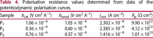
These results are in agreement with the current density and corrosion potential results obtained in the polarisation tests for the P3 sample. From the data presented in Table 4, it can be observed that, with respect to the polarisation resistance (R p) calculated by Equation (7), the P3 sample has a better result in terms of corrosion resistance, followed by P1 and P2 samples.
Correlation between electrochemical behaviour and solidification microstructure
By comparing the Bode diagram and Nyquist plots (Figure 5) and the fitted results obtained from the equivalent circuit (Table 1), it can be seen that the Sb content of the examined samples of three different Sn–Sb alloys and the non-equilibrium solidification conditions played an important role on the microstructure formation, thus significantly affecting the resulting electrochemical behaviour of each sample. Samples with different Sb contents but with similar average values of cell spacings (λ c = 19.7, 20.3 and 19.9 µm) were chosen to perform the electrochemical tests, to permit only the influence of alloy Sb content and non-equilibrium solidification conditions on the resulting microstructural features to be investigated. Their microstructures are characterised by SnSb particles homogeneously distributed throughout the β-Sn matrix (Figure 4(b)), with a unique differentiation for the P3 sample that contains one more intermetallics in its composition (Sn2Sb3). One more factor should be considered: the IMC presence into the Sn matrix of all analysed alloys could result in the formation of several galvanic couples. From the electrochemical point of view, considering the phases detected by XRD, at least three distinct galvanic couples are clearly formed for the P3 sample, which are: β-Sb//SnSb, SnSb//Sb2Sn3 and, β-Sb//Sb2Sn3, whereas for P1 and P2 samples there is only one couple (β-Sb//SnSb), resulting in a potential difference between β-Sb and the SnSb IMC sites. Once the SnSb IMC is constituted of 50% of Sn and 50% of Sb, and the Sb2Sn3 IMC is formed by 49% of Sn and 51% of Sb, it is possible to calculate the approximated potential values for each galvanic couple, which can be determined by the following formulas:


The approximated potential for the SnSb IMC is −400 mV (SCE) and that of the Sb2Sn3 IMC is −405.4 mV. These values can be used to estimate the potential difference of the galvanic couple. The galvanic couple β-Sb//SnSb has an E = −140 mV – (−400 mV) = 260 mV, the SnSb // Sb2Sn3 has an E = −400 mV – (−405.4 mV) = 5.4 mV and, the β-Sb // Sb2Sn3 has an E = −140 mV – (−405.4 mV) = 265.4 mV. For P1 and P2, the set β-Sb//SnSb represents a potential gap of −140 mV // −400 mV.
Once the β-Sb matrix has a nobler potential as compared to the SnSb and Sb2Sn3 IMCs, the corrosion sites where the IMCs are present show more severe corroded areas. Also, the IMCs are regions with higher Sb content, that is, regions with presence of IMCs tend to corrode the microstructure, which leads to detachment and incorporation into the corrosion product, as shown in Figure 8 for all analysed samples. Figure 8(b) (P2) shows intense corrosion sites associated with regions with higher Sb concentration, as compared to samples P1 and P3. This result agrees with the previously discussed results of XRD, since the presence of the SnSb IMC in sample P2 is more prominent with 11 peaks attributed to its crystalline phase, against 7 peaks to P1 and 8 peaks to P3 samples (Figure 3).
Related to the P3 sample there are 3 galvanic couples, of which two of them: β-Sb//SnSb and β-Sb//Sb2Sn3 have similar potentials of 260 and 265.4 mV, respectively, while the SnSb//Sb2Sn3 couple has the noblest potential of 5.4 mV. By the XRD analysis (Figure 3(c)) it is possible to identify 8 peaks related to the Sb2Sn3 IMC, 8 peaks to the SnSb IMC and 8 peaks to the β-Sb matrix. This indicates an equal distribution of galvanic cells in the alloy, with a more widespread corrosion, as shown in Figure 8(c), where there is no detachment of IMCs from the alloy surface, and the same occurs to the P1 sample, and unlike happens to the P2 sample.
According to what was mentioned before, the lowest capacitive arc is attributed to P2, while the intermediate capacitive arc was identified as that of the P1 sample and, the higher capacitive arc is related to the P3 sample, which has SnSb and Sn2Sb3 IMCs precipitates disseminated by the β-Sn matrix, according to the SEM image of Figures 4 and 8 and the XRD patterns of Figure 3.
Considering the corrosion characteristics, it can be affirmed that the microstructure morphology and the type and distribution of the IMCs played an important role on the electrochemical corrosion resistance. The present results gave indications that with the increase in the alloy Sb content towards near peritectic compositions (sample P3), the corrosion resistance tends to be improved. Comparing P1 and P2 samples separately, it can be observed that the P1 sample has better corrosion resistance than P2, despite the higher Sb concentration of P2. This can be attributed to the higher fraction of SnSb particles of sample P2, which are distributed throughout the β-Sn matrix.
The highest corrosion resistance of the P3 sample, despite being associated with a higher alloy Sb content, is related to the presence of a different IMC in the alloy microstructure coexisting with the SnSb IMC previously observed in P1 and P2 samples, that is, the Sn2Sb3 IMC into the P3 sample, which is formed under non-equilibrium solidification conditions, attributes a better corrosion resistance to the sample, once it can establish a potential balance between the galvanic couples across the sample.
SEM images were performed after polarisation tests for all Sn–Sb alloys samples and can be observed in Figure 9. From the polarisation plots and SEM images, it is possible to observe that the P3 sample shows a higher frequency of pit nucleation (indicated by red circles in Figure 9(c)) and this can be attributed to its the smallest E pass – E pitting range (−177 mV). It is also possible to observe sites of a more generalised corrosion throughout the thin oxide film when comparing P1 and P2 samples. The P2 sample (Figure 9(b)) shows the intermediate pitting sites corresponding to its intermediate E pass – Epitting range (−222 mV). The P1 sample has the smallest number of pitting sites (Figure 9(a)) among all examined samples and this is directly attributed to its E pass – E pitting range (−321 mV).
SEM images of Sn–Sb alloys samples after the polarisation tests: (a) P1: Sn–2wt-%Sb, (b) P2: Sn–5.5wt-%Sb and (c) P3: Sn–10wt-%Sb.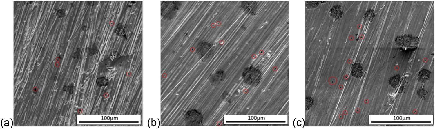
Conclusions
The corrosion resistance of Sn–Sb alloys has been investigated by EIS, equivalent circuit and linear polarisation and the results correlated with microstructural features of hypoperitectic and hyperperitectic Sn–Pb solder alloys. The measurements obtained by these analyses indicated that the hyperperitectic Sn–10wt-%Sb alloy sample has the highest corrosion resistance as compared to hypoperitectic samples: Sn–2wt-%Sb and Sn–5.5wt-%Sb. It was shown that the increase in the alloy Sb content promotes changes in the nature, size and morphology of the Sn–Sb intermetallic particles (IMCs), consequently affecting the resulting corrosion resistance.
The EIS quantitative data indicated that the Sn–10 wt-%Sb sample is associated with the best corrosion resistance because of the high resistance related to its oxide barrier layer. The polarisation curves indicated that the lowest corrosion current density and nobler potential were those of the Sn–10 wt-%Sb alloy sample, which was also confirmed by calculations of polarisation resistance.
The XRD data showed that the alloy Sb content has a directly influence on the IMC formation, i.e. the hypoperitectic alloy samples have only the SnSb IMC, while the Sn–10wt-%Sb alloy, shows the coexistence of SnSb and the Sn2Sb3 IMCs, both randomly distributed throughout the cellular Sn-rich matrix. The simulations provided by the equivalent circuit, showed that the presence of the SnSb IMC has a determining influence on the corrosion resistance, and its presence in greater amount in the Sn–5.5wt-% Sb alloy sample led to a lower corrosion resistance as compared to that of the Sn–2wt-% Sb alloy sample. The increase in the Sb alloy content towards the hyperperitectic range (Sn–10wt-% Sb alloy) leads to the formation of both the SnSb and the Sb3Sn2 IMCs. It was shown that the presence of the Sn2Sb3 IMC improves the corrosion resistance, making the hyperperitectic sample to have the best corrosion resistance of all analysed samples.
Footnotes
Disclosure statement
No potential conflict of interest was reported by the author(s).