
Abstract
Rigid and flexible, pixelated ultraviolet photodetectors (PD) based on ZnO have been fabricated by material extrusion 3D printing technique. The photoresponse is studied in an out-of-plane configuration. An open lattice structure is printed using PLA over ITO/Glass substrate for rigid, and TPU over ITO/PET substrate for flexible PDs. ZnO slurry is filled selectively into the columnar matrix by the microdispensing technique. The optical detector printed on ITO/Glass substrate shows a sensitivity of 25 and responsivity of 1.55 nA/mW with a rise and decay time of 1.6 and 0.6 s, respectively. Similarly, the flexible PD printed using TPU lattice shows a sensitivity of 9.5 and responsivity of 0.38 nA/mW with a rise and decay time of 1.8 and 0.6 s, respectively. The charge transport mechanism is studied using band diagram analysis. 3D printed open lattice structure is found to be a potential template for sensor fabrication. This work demonstrates the capability of material extrusion 3D printing with an open lattice structure for the fabrication of high-resolution pixelated PDs.
Introduction
Additive Manufacture (AM) is revolutionizing the method of developing complex 3D models for applications in the medical field like prosthetics, bioprinting, orthotics, etc.,1,2 electronic field for wearable sensors, lab on a chip, etc.,3,4 and automobile industry for developing spare parts for engines and turbines like crankshaft design, etc.5–10
The electronic component industry has been projected to have exponential growth, and 3D printed electronics will have a significant contribution. 11 3D printed electronics is primarily used to create prototypes but can also pave a path for the fabrication of complex electronic devices in the future. It has the advantage of mass production, low cost, and ease of processing with greater freedom of design and customization as required by the electronics industry. Even though AM lacks the resolution compared with micro and nanofabrication, it is envisioned to be next-generation technology due to its current progress and optimization for batch fabrication. Also, the availability of a wide variety of materials gives us the freedom to move from conventional fabrication technique, which is very limited in terms of feedstock materials.12,13 Inkjet and Aerosol jet printing AM techniques are used widely for 3D printed electronics compared with filament-based extrusion techniques, mainly due to nondirect contact printing on both planar and nonplanar surfaces. These techniques are used primarily to print sensors, antennae, and other functional electronics onto plastic, glass, and ceramic substrates.14,15
Lu et al. fabricated electrodes for solid-state supercapacitors. 16 Wu et al. fabricated carbon nanotube thin film transistors, 17 and Kang et al. fabricated passive components like resistors, capacitors, and inductors by the inkjet printing technique. 18 Skarzynski et al. fabricated highly conductive circuits using silver nanoparticles ink by aerosol jet printing. 19
Material extrusion is a widespread and readily available low-cost technique for layer-by-layer 3D printing, primarily based on polymers but spread even to metal and ceramics. Both microdispensing and fused deposition modeling (FDM) are extrusion-based techniques, and there is a vast library of feedstock material available compared with other 3D printing techniques.20–23
The extrusion-based 3D printing technique is the emerging technology for prototyping electronic and functional devices such as photodetectors (PDs), LEDs, and strain sensors,14,24,25 using various functional materials without high-end cleanroom fabrication techniques. FDM, also called Fused Filament Fabrication is the most commonly used method of 3D printing. It allows for the direct writing of nonconductive/conductive thermoplastic polymers, such as PLA, acrylonitrile butadiene styrene (ABS), and their composites, of metals and semiconductors by fusing and depositing layer by layer. 26 It is available readily for industrial applications, and there is a lot of scope for FDM-printed devices with high resolution to meet the demands of the electronic market.
Innovative methods using FDM 3D printing can play a huge role in the electronic industry. Using the FDM technique, Maurel et al. studied 3Dimensional LiFePO4/Graphite Battery, 27 Yang et al. deposited polymer nanocomposites for Electromagnetic Interference Shielding applications. 28
Infill pattern is very important for the mechanical and structural integrity of 3D printed models, especially for aeronautics, automobile, and prosthetics.29,30 These lattice structures are inspired by nature, which has been adopted through the process of evolution. 31 Rivera et al. found that beetles have a specific arrangement of flakes laminated microstructure and withstand heavy loads, which can find application in body armor. 32 The same can be inspired by the super hydrophobicity of water strides 33 and the biophotonics of peacock feathers. 34 Using Design for Additive Manufacturing, different lattice structures can be simulated for different parts of the models as per the requirement of mechanical, thermal, and electrical properties for lightweight with no compromise of structural integrity. 35 Material selection, along with design, determines which lattice structure is feasible.36,37 Several lattice types are available with commercial slicer softwares, such as gyroid, rectilinear, grid, honeycomb, triangles, Hilbert curve, etc., based on the requirement for specific properties and functionality of the model.
As such, lattice printing is known in literature where an STL file of the desired lattice is modeled by computer-aided desgin (CAD) software and printed. This kind of lattice-based printing has found applications in electrodes for membrane fuel cells, water splitting, electrochemical cells, etc.27,38,39
Ultraviolet (UV) PDs have received a lot of interest due to their applicability in industrial, environmental, and even biological domains for flame and radiation detection, biochemical detection, solar flare detection, space communications, air purification, and ozone sensing.13,40
The optical sensor market is currently dominated by silicon-based PDs due to their high performance, broad spectral sensitivity, and ease of integration with electronics. However, Si-based PDs suffer due to high noise contribution arising from dark currents, expensive device fabrication process, and device aging.41,42
There is a wide range of materials available for UV detection like perovskites, silicon derivatives, metal halides, transition metal di-chalcogenides, and metal oxides.43,44 However, semiconductor-based metal oxides such as ZnO, SnO2, Ga2O3, WO3, and TiO2 are proven to be the preferred materials for UV detection due to wide band gap, ease of fabrication, 45 scalability, control over crystal orientations, uniformity, and reproducibility. They also have a direct band gap with large exciton binding energy leading to low dark current and stability.40,46
In particular, ZnO exhibits a wide bandgap of 3.34 eV and n-type semiconductor behavior with exciton binding energy of ∼60 meV, making it a promising material for optical sensing in the UV-A region.47–49
Although there are very few reports on fabricating PD by FDM printing, they lack resolution and flexibility. Also, the much-desired device density for easy integration with commercial electronic devices is far fetched. Lee et al. fabricated a PD based on ZnO by a conductive filament of Ag by using FDM. 50 Park et al. have shown PD built on planar and nonplanar substrates based on conductive polymer by extrusion-based technique, 51 but for commercialization and meeting the market demands, 3D printing has to be evolved to make products more compact and miniaturized. As such, there are no reports on using infill lattice as a template for the fabrication of PDs.
In this study, we have shown a very compact and densely pixelated PD fabricated by FDM technique, exploiting the infill lattice pattern. We used commercially available ITO/glass substrate, which is being extended to flexible conductive substrates as electrodes onto which 3D models are built. The open lattice structure is printed by selecting zero, bottom, and top layers for photoactive material impregnation. Based on the infill percentage, the pixel density can be controlled to make the device compact and can have a wide selection of materials for wide spectral photo response. This kind of infill pattern takes the FDM printing ability to fabricate devices to their maximum resolution, and this is not reported in the literature to our knowledge. Hence, the present work can prove a game changer for the fabrication of sensors by FDM printing.
Experimental Section
Additive manufacturing setup
The 4DS Smart One, a dual extruder FDM 3D printer by Adroitec Ltd., is used for fabricating 3D printed PDs. ITO/Glass substrate of dimension 25 × 25 × 5 mm3 with resistivity 12–20 Ω/sq and 76% transmission and Indium tin oxide-coated PET having a resistivity of 60 Ω/sq having transmission of 78% are used as build plates for 3D printing.
Figure 1 shows the schematic of the modified build platform with ITO substrates at nine different points for bed leveling and 3D printing, along with the impregnation of photoactive material using a syringe. Bed leveling was done using multipoint mesh leveling mode. In this mode, a value of n = 3 is chosen for which a total of 3 × 3 points are identified covering the entire bed and returns the command to the leveling interface. To target the ITO substrate as a build plate for 3D printing at the center of the platform, eight other similar ITO pieces at respective points of the probe-touch sensor are placed as shown in the schematic of Figure 1a and b. Figure 1b shows the schematic of faded images of the extruder/touch sensor along with the path followed, depicting the movement of the extruder across nine different points, with “i” being the initial and “f” being the final position. After calibration, the extruder comes to the center stage onto the ITO substrate for printing. Figure 1c shows the cartoon of the 3D model printed at the center onto the ITO substrate. Figure 1d shows the 3D model with an open lattice selectively impregnated with photoactive material.
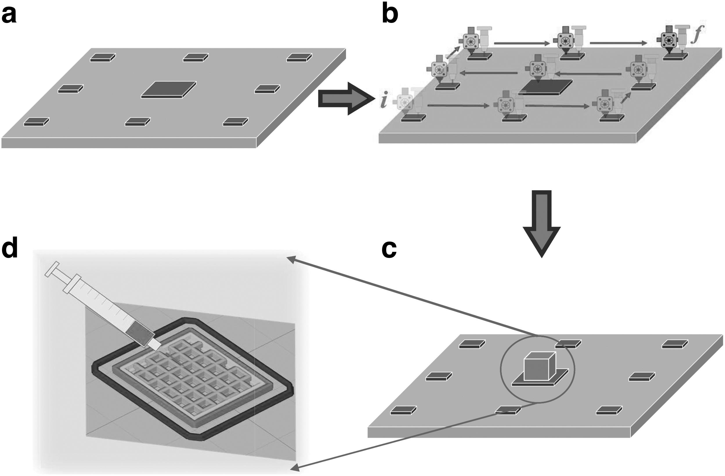
Schematic for 3D printing of open lattice structure over the transparent conductive substrate and impregnating with photoactive material slurry.
Design and fabrication of pixelated template
PLA spool from Sigma-Aldrich is used for printing open lattice 3D models. 3D printing is done by taking a CAD file, converting it into an STL file, and slicing the 3D model layer by layer using slicer software. For 3D printing of PLA over ITO/glass, the extruder temperature and the bed temperature are set to 200°C and 70°C, respectively. Increased bed temperature enhances the adhesion of PLA to the ITO glass substrate. For printing TPU over ITO/PET, the extruder and bed temperatures are set to 200°C and 50°C, respectively. For printing an open lattice and exposing the infill pattern, the number of top and bottom layers are kept at zero. The layer height is maintained at 220 μm with two shells for the outer perimeter. A grid pattern is used as the infill pattern for the 3D model. An infill density of 80% with a fill angle offset of 0° and 90° for alternative layers is set to get a lattice pattern. Three skirt layers are printed to prime the extruder before printing the model. For the fabrication of PDs, cuboid 3D models with dimensions 10 × 10 × 1.5 mm3 are printed.
Instant glue is used along the periphery at the interface of the ITO and 3D model to avoid any dislodging of the 3D model from the ITO substrate during sample filling and making electrode contacts. The speed of printing is also decreased by almost half the speed of conventional PLA printing. 52
PD design and fabrication
ZnO powder is used as a photoactive material for making PDs. ZnO powder of size ∼1 μm is purchased from SRL (Sisco Research Laboratories Pvt Ltd.). A slurry of ZnO is prepared by mixing with deionized water in 1:2 w/w. The ZnO slurry is transferred to a syringe and is used to selectively fill the pixels of the open grid pattern of the 3D model under the microscope. The process is repeated with intermittent evaporation of water at room temperature until the pixels are filled with the slurry. As the ITO substrate onto which the 3D model is deposited is used as a transparent electrode for exposure to light, the other side of the 3D model is deposited with Al foil as a counter electrode. The Al foil used for the counter electrode is purchased from Alfa-Aesar, having 0.2 mm thickness and 99.9995% purity. For the precise bending angle measurement, a “2-Jaw Vise with swappable jaws” is 3D printed by ABS.
Measurement and characterization
Mechanical analysis of TPU and its mesh structure is done using Dynamical Mechanical Analyzer (DMA 8000) of PerkinElmer for a temperature range from −40°C to 40°C in dual cantilever bending mode at a heating rate of 2°C/min with constant frequency of 1 Hz using liquid nitrogen as the immersion fluid. For current–voltage (I-V) measurements of the fabricated PD, a source measure unit (Keithley-2602A) is used with a Test Script Builder Program (TSP). Using TSP, a voltage sweep of −2 V to 2 V in 10 mV increments is programmed and applied to the device for IV characteristics under dark and UV illumination. A UV LED with a power density of 189 mW/cm2 and a wavelength of 370 nm is used as an illumination source. A silicon PD S120VC connected to a digital power and energy meter PM100D from Thorlabs is used to calibrate the UV LED source.
Results and Discussion
Manufacturing and analysis of structure
Among all lattice structures available on commercial slicer software, grid, honeycomb, and triangular lattice provide periodic and uniform columnar pores with no interconnection from pore to pore. This aspect of independent columnar pore formation from the bottom of the structure to the top, using a grid lattice, is explored in the present work for the fabrication of pixelated PDs. Figure 2 shows the comparison of the rectilinear infill lattice pattern with that of the grid lattice. Even though rectilinear lattice is a more popular and commonly used lattice infill, it has interconnected and permeated pores. Figure 2c and d shows 3D printed models with rectilinear and grid lattice infill, respectively. During the 3D printing of the model with rectilinear infill, the layer-by-layer deposition happens by bridging the preceding layer as shown in Figure 2a, leaving permeated pores, as in Figure 2c. For models printed with a grid lattice infill, the layer-by-layer deposition happens conformally to the orthogonal bottom layer as shown in Figure 2b making columnar pores with no interconnection, as in Figure 2d.
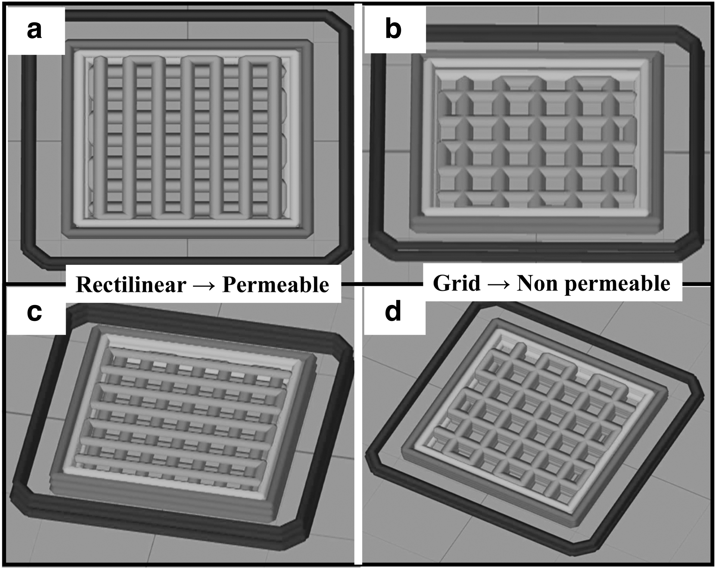
Images of both rectilinear and grid lattice structures after slicing for layer-by-layer 3D printing. An initial layer of both
This conformal patterning also increases the contact surface area of the model with the substrate and improves the adhesion. The contact area increases by almost double with the grid lattice infill pattern. Due to this conformal deposition and columnar pore formation, grid lattice-based infill models can potentially be used as microvials for holding inks and pastes without permeation.
Figure 3 shows the grid lattice infill 3D model using PLA on an ITO/glass substrate for its lattice size analysis. To use ITO as bottom electrode, FDM printing is done directly on to ITO/glass substrate without using bed adhesive. Figure 3a shows the sliced image of an open 3D model with 80% infill. For making it an open lattice, both the top and bottom layers are made zero, and no raft is chosen. Figure 3b shows the printed 3D model of dimensions 10 × 10 × 1.5 mm3. PLA is known to have good adhesion to the substrate, but to avoid dislodging of the model from the substrate during material deposition and electrode contacts, an acrylate glue is applied around the periphery at the interface of the ITO substrate. Figure 3c shows the optical image of the lattice model for top view. Using ImageJ software, both the percentage of opening and the pore size analysis are done. The total coverage of the PLA in terms of orthogonal lattice strands and boundary walls of the model is ∼69% making it 31% transparent.
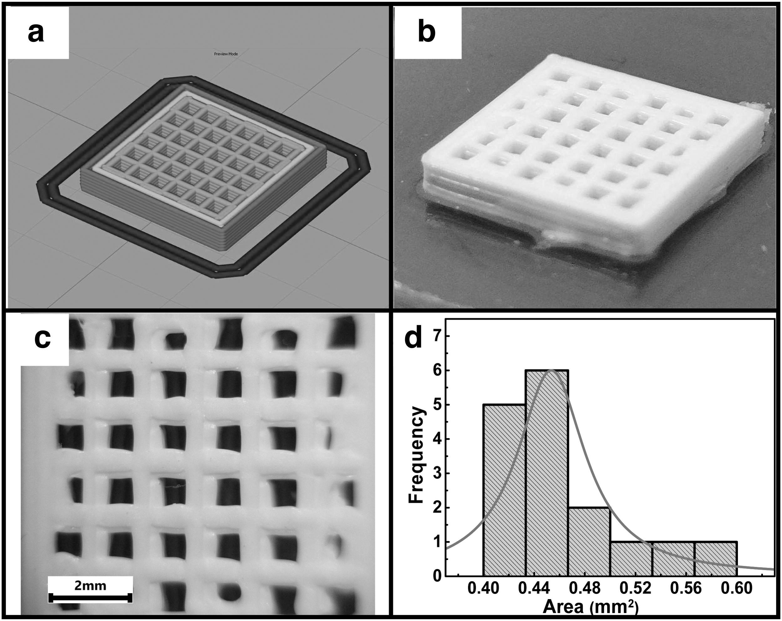
Images of open lattice model after slicing and printing along with microscopic image and histogram analysis of pores.
From the histogram analysis, the pore size of the columnar lattice structure is 0.44 mm2 corresponding to 660-μm-wide square pores. The lateral resolution known by FDM printing is 400–500 μm 53 and with 80% infill, we achieved the maximum pixel resolution possible by FDM technique. Any more increase in infill percentage will make the lattice irregular and will not be columnar for photoactive material impregnation.
Figure 4 shows DMA analysis of 3D printed TPU structures both with solid infill and grid with 80% infill. DMA analysis gives both storage and loss modulus of the structures giving information about mechanical response to oscillating stresses and/or strains with temperature. Glass transition temperature (Tg) and Modulus of elasticity (E) of the samples are studied. Storage modulus corresponds to the stored energy elastically against applied force and Loss modulus corresponds to the damping. Tan δ, which is a ratio of loss to the storage modulus of material, gives information about the glass transition temperature at which the material undergoes the transition from glassy to a soft state.
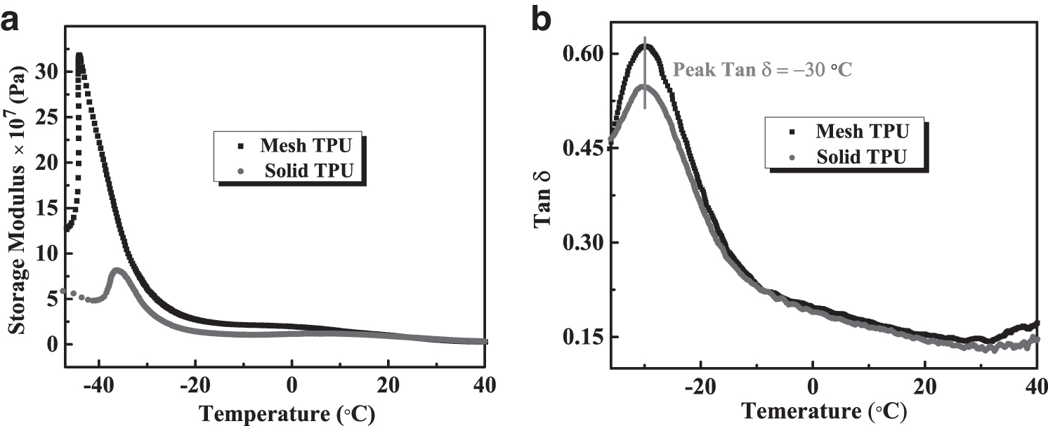
DMA curves of TPU solid and mesh structure,
Figure 4a shows the behavior of storage modulus for both samples against temperature and Figure 4b shows the Tan δ versus temperature. From Figure 4a of storage modulus, no plateau is observed below −20°C, indicating an amorphous phase. A plateau region corresponding to the linear viscoelastic region (LVR) is observed beyond −20°C (Fig. 4a), indicating the rubbery stage. The storage modulus is found to be enhanced with 80% infill mesh structure, which is 4 orders of magnitude more compared with solid infill at temperatures below −30°C (Tg) and ∼2 orders of magnitude in the linear region above Tg.
Material stiffness or resistance to deformation under applied stress can be measured through the modulus of elasticity. Knowing the Poisson's ratio (ν), the modulus of elasticity can be calculated from the storage modulus, using the equation: E = E′/(1 − ν 2 ), where E is the modulus of elasticity, E′ is the storage modulus, and ν is the Poisson's ratio of the material. Considering Poisson's ratio of 0.39 for TPU, 54 the calculated modulus of elasticity of the mesh structure is 24 MPa for the LVR, 55 which indicates the soft nature of the TPU used for making flexible PDs.
PD characterization
Figure 5 shows the fabricated 3D printed pixelated PD by FDM printing, lattice filling by ZnO, along with its IV characteristics.
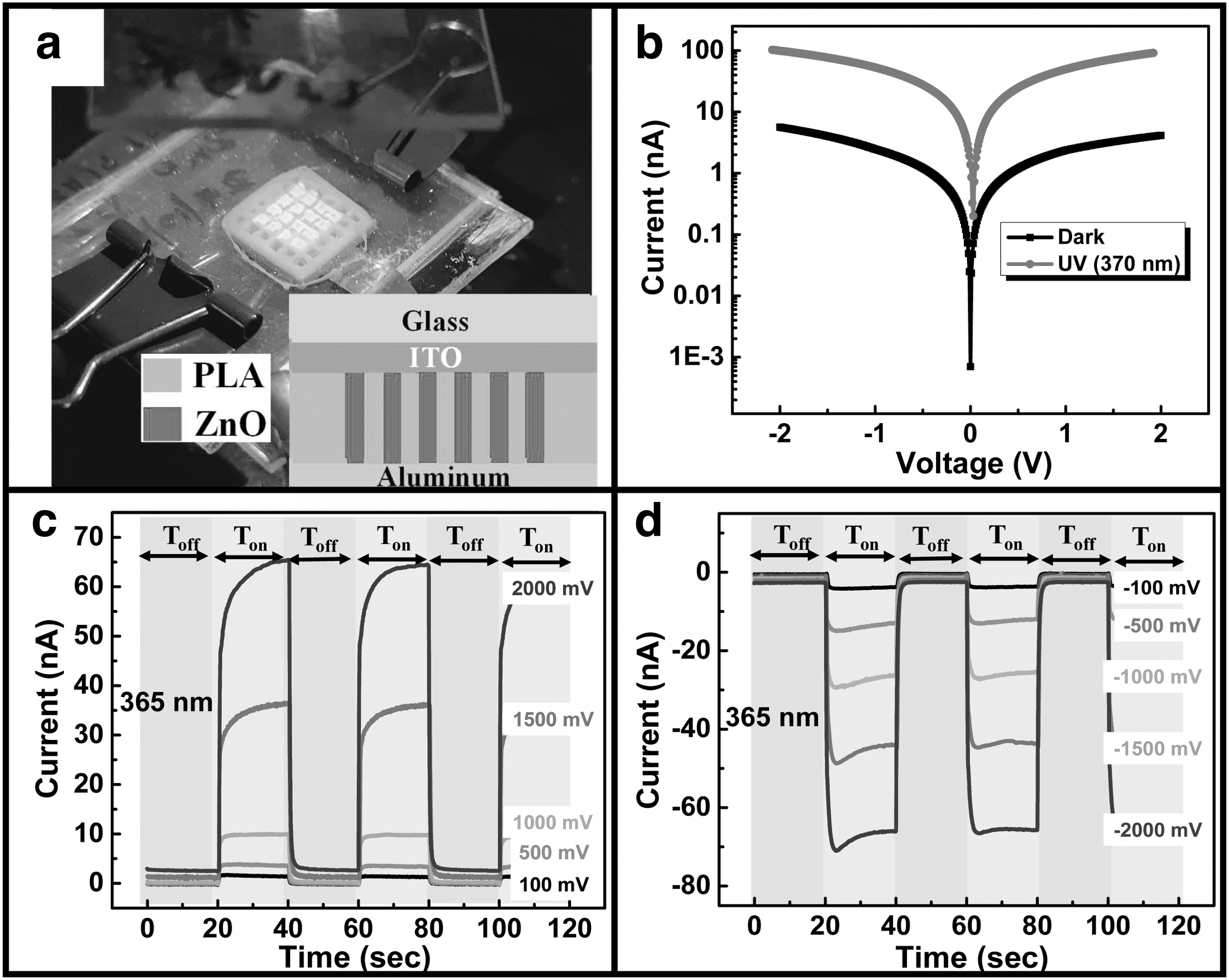
IV characteristic and photoswitching response of ZnO/PLA device with out-of-plan contacts.
Figure 5a shows the device under testing for UV illumination. The 6 × 6 array 3D printed lattice with a 4 × 4 array of filling with ZnO is seen in Figure 5a. The inset of Figure 5a shows the schematic of the cross-sectional profile of the device. The top side facing UV illumination is ITO-coated glass substrate with ITO in contact with ZnO. The other side of the electrode system is an aluminum foil completing the circuit forming ITO/ZnO/Al, a metal−semiconductor−metal junction.
Figure 5b shows the IV characteristics of the device under dark and UV-A illumination for a continuous sweep of voltage from −2 to +2 V with a sweep resolution of 0.01 V. The current is plotted in a logarithmic scale, and a current of magnitude 100 nA is observed for the maximum voltage of +2 V. The IV characteristic is symmetric for both +ve and −ve sweeps with more or less similar magnitude for both polarities. This symmetric behavior of the IV sweep describes the ohmic nature of contacts with ZnO.
Figure 5c and d shows the pulsing behavior of the PD for both + ve and −ve bias and for different magnitudes, ranging from 100 mV to 2 V. The pulsing is done at an equal interval of 20 s for both on and off time. The enhancement factor of the PD is calculated by
Figure 6 shows the voltage-dependent device characteristics at different biases ranging from 100 to 2 V for different parameters like Responsivity, Detectivity, Noise Equivalent Power (NEP), and External Quantum Efficiency (EQE).
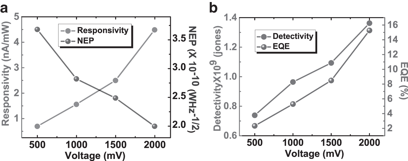
Responsivity, Detectivity, NEP, and EQE of the photodetector at different biases ranging from 100 to 2000 mV.
Figure 6a shows the responsivity and NEP plotted against the voltage. The responsivity of the PD is defined as the efficiency to convert the optical energy into electrical energy, and for a discrete wavelength of incident light and for a fixed bias, the responsivity is given by R = (IUV − Id)/(Pin. A), where Pin is the power density of incident light, A is the active area of the device, Id is the dark current and IUV is the current under illumination. From Figure 6a, the responsivity at a bias of 2 V of the device with an active area of ∼7.38 mm2 is 4.48 nA/mW under UV (370 nm) illumination of 189 mW/cm2. NEP is the minimum optical power required by the detector to have a signal-to-noise ratio of one and is calculated by NEP = [(2eId)1/2/R]. For 2 V of applied bias, the NEP of the device is 1.99E-10 W·Hz−1/2.
Figure 6b shows the Detectivity and EQE of the PD. The EQE is the ratio of the number of electrons in an external circuit to the number of incident photons and is given by EQE = Rhc/λq, where R is responsivity, Id is the dark current, h is Planck's constant, c is the speed of light, λ is the wavelength of the incident light (370 nm), and q is the elementary charge. The EQE for the device at 2 V is 15.3%. Similarly, the Detectivity at 2 V bias, which is the capacity to detect weak signals against detector noise given by D = [R.A1/2/NEP.(2eId)1/2], is 13.6E-8 Hz−1/2·W−1. The above data are in agreement with general PD characteristics where the NEP decreases and EQE increase with an increase in applied voltage. Similar behavior is observed for −ve voltage sweep, where the responsivity, detectivity, and EQE increase linearly and NEP decreases with an increase in the bias of the PD.
Figure 7 shows the band diagram of Al/ZnO/ITO heterostructure for the electron transfer mechanism in 3D printed lattice-filled ZnO PDs. Figure 7a–c show band alignment at Al/ZnO, ZnO/ITO interfaces for 0, +2, and −2 V of applied voltage at the ITO electrode of the device with respect to the Al electrode. The work function of Al, ϕAl is 4.2 eV, 56 and ITO, ϕITO is 4 eV (3.5–4.3 eV). 57 The band gap (Eg) of ZnO is 3.39 eV, 48 and the electron affinity (χ) is 4.3 eV. ZnO is an inherently doped n-type semiconductor. The oxygen in the tetrahedral structure unit cell is offset, and this noncentrosymmetry 48,58,59 of the oxygen atom gives rise to polarity and is inherently doped.
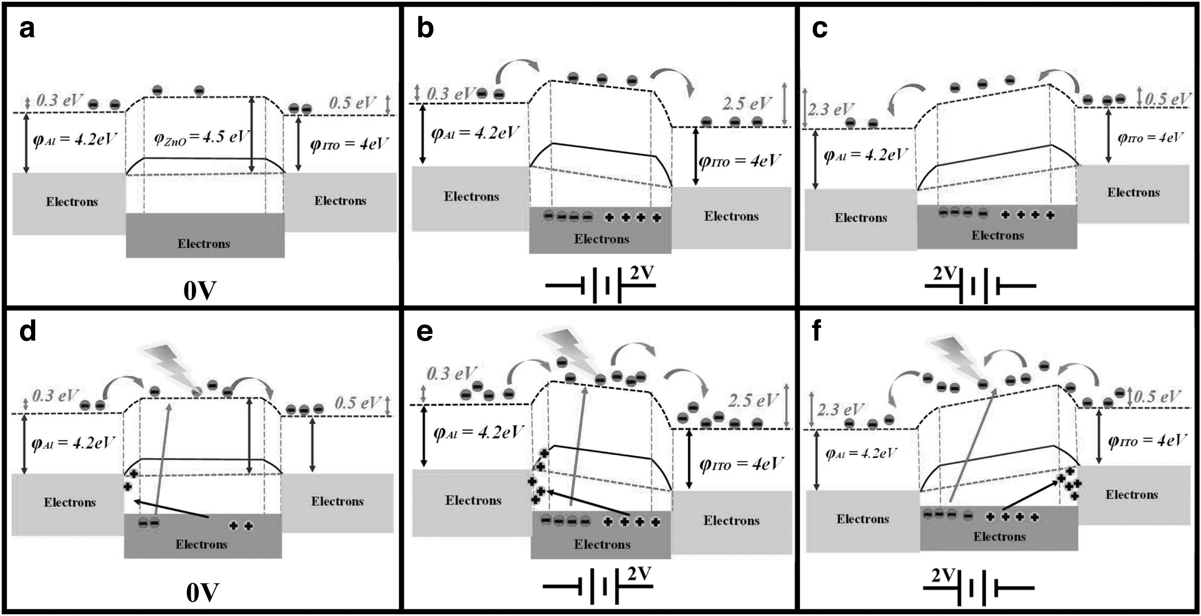
Schematic energy level diagrams for pixelated Al/ZnO/ITO UV photodetector. Six
Considering the position of the Fermi level (EF) and the electron affinity (χ), the work function of the ZnO, ϕZnO is 4.5 eV. 60 As the work function of ITO and Al, ϕAl and ϕITO are less compared with ϕZnO and ZnO being n-type, the band bending at the interface of ZnO with Al, and ITO forms an accumulation region, and the flow of charge carriers is nonrectifying and ohmic. The same is observed from the IV characteristics of the device in Figure 5b. In the absence of bias and under illumination, photoexcited charge carriers will further increase electron density in the conduction band. Under bias, the band bending further increases due to potential gradient, and the current in the device increases as shown in Figure 7d. For the −ve bias applied to the ITO electrode, the Fermi energy level increases on the ITO side, and electrons flow toward the Al electrode as shown in Figure 7e, and for the +ve bias, the Fermi energy level decreases, and electrons flow from Al to ITO as shown in Figure 7f. This is further enhanced by incident light matching the band gap creating charge carriers and an increase in charge carrier density.
As the work function of Al and ITO are similar, the IV characteristics of the device for voltage sweep are symmetric for both +ve and −ve bias, as shown in Figure 5b.
The merit of the 3D printed lattice structure for flexible and pixelated UV PDs is realized by printing an elastomeric material. To achieve this, the printing material has been changed from PLA to TPU, the substrate has been changed to ITO/PET, and Ag thin film deposited physically as the counter electrode. The ITO/PET acts as a transparent and flexible electrode. Figure 8a shows the flexibility of one such 3D printed TPU grid lattice onto the ITO/PET substrate. As the PET and TPU are both flexible, the model can withstand the stress generated during bending, and the adhesion is good enough to hold the model without being dislodged from the substrate. Compared with PLA, it is observed that TPU has excellent adhesion to ITO-coated PET and can withstand flexing and bending without any external adhesive at the periphery. For controlled bending and studying device behavior at fixed angles, a 3D printed two-jaw vias is used. Figure 8b shows the TPU lattice-based PD on PET substrate, clamped between two jaws of the vias with an inset showing the cross-section of the device at an angle under bending.
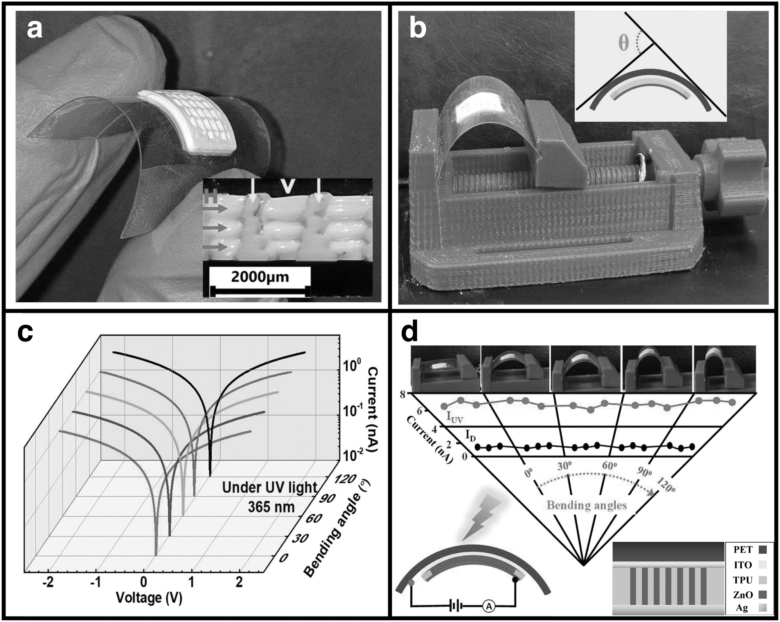
Measurement of ITO/PET flexible photodetector device.
Figure 8c shows the 3D plot of the IV characteristics of the flexible PD for different bending angles. The x-axis of the plot shows the voltage sweep from −2 to +2 V, and the y-axis shows different bending angles from 0° to 120° at 30° interval. The magnitude of the current varies from −6 to +6 nA, as shown along the z-axis in the logarithmic scale. The IV characteristics have shown that the voltage-dependent current is linear and symmetric for both forward and reverse bias. Also, the IV characteristics are independent of the stress generated on the device through bending. The IV characteristics are similar for all bending angles up to 120°, which is the desired feature for flexible PDs.
Figure 8d shows the current stability of the PD under bending at different angles for a bias of 2 V. The topmost figure shows the array of PD images under bending at different angles of 0° to 120° with both on and dark current. The scattered plot in red depicts the photocurrent under UV illumination, IUV, whose magnitude is 6.2 ± 0.2 nA, and the scattered plot in black shows the current of the PD in the dark. The inset of Figure 8d shows the schematic of the flexible PD with applied bias and UV illumination under bending, along with the cross-sectional profile of the device. The transparent PET substrate faces UV LED for illumination with ITO in contact with ZnO filled in the 3D printed TPU lattice. The device is bent inward to change the bending angle, with Ag film acting as the bottom electrode. As observed from Figure 8d current behavior, the on-current at 2 V bias is highly stable without any effect of bending on its characteristics. This confirms the stability of the PD both in the dark and under illumination.
A comparison of photoresponse parameters of various conventional and 3D printed ZnO PDs in the classical regime is listed in Table 1. The rise and decay time of the PD is shown for different configurations of ZnO devices and has been compared. Compared with the parameters of various PDs, as shown in Table 1, both the PDs reported in this work shows an improved response time. From the literature, there is no data on the response time of the FDM printed ZnO PDs, whereas the response time is high for the conventional PD compared with our present work. The out-of-plane configuration of the device assisted by a template 66 in the form of a 3D printed lattice will enhance the device response time. However, the response time is high compared with the devices fabricated by high-end techniques like inkjet and aerosol jet printing64,65 and by conventional micro and nanofabrication techniques.
Comparison of ZnO Photodetector Fabricated by Different Conventional and 3D Printing Techniques with Their Rise and Decay Time
3DP, 3D printing; FDM, fused deposition modeling; NPs, nanoparticles; RF, radio frequency.
Conclusion
A pixelated UV rigid and flexible PD based on ZnO is printed with the FDM 3D printing technique. The infill pattern of the 3D printing technique is exploited for making pixelated and high-resolution PDs possible with the FDM technique. Different lattice structures are examined and grid lattice is used to get nonpermeable columnar pores for microvials and reservoirs. These pores are filled with photoactive material by dispensing technique. These 3D printed PDs are studied for their IV characteristics and time-dependent photoresponse. The charge transport mechanism is studied using band diagram analysis of ITO/ZnO and ZnO/Al interfaces for the nonrectifying behavior of IV characteristics. The work has been extended to a flexible PD using ITO/PET as a flexible substrate and TPU for making a lattice structure. Furthermore, for commercial applications, the simplicity of the infill pattern for customization of PDs with high throughput possible with the FDM 3D printing process is emphasized.
Footnotes
Authors' Contributions
B.P.B.: methodology, investigation, formal analysis, writing—original draft, review and editing, and data curation. V.T.: supervision, conceptualization, visualization, formal analysis, and writing—original draft, review, and editing. S.R.D.: funding acquisition and resources.
Author Disclosure Statement
The authors declare that they have no affiliations with or involvement in any organization or entity with any financial interest (such as honoraria; educational grants; participation in speakers' bureaus; membership, employment, consultancies, stock ownership, or other equity interest; and expert testimony or patent-licensing arrangements), or nonfinancial interest (such as personal or professional relationships, affiliations, knowledge, or beliefs) in the subject matter or materials discussed in this article.
Funding Information
B.P.B. acknowledges the Council of Scientific and Industrial Research (CSIR) and Academy of Scientific and Innovative Research (AcSIR) for fellowship and academic support. V.T. acknowledges CSIR for financial support under Laboratory Project and in-house R&D support.