
Abstract
Significant advancements in waveguide technology in the mid-infrared (MIR) regime during recent decades have assisted in establishing MIR spectroscopic and sensing technologies as a routine tool among nondestructive analytical methods. In this review, the evolution of MIR waveguides along with state-of-the-art technologies facilitating next-generation MIR chem/bio sensors will be discussed introducing a classification scheme defining three “generations” of MIR waveguides: (1) conventional internal reflection elements as “first generation” waveguides; (2) MIR-transparent optical fibers as “second generation” waveguides; and most recently introduced(3) thin-film structures as “third generation” waveguides. Selected application examples for these each waveguide category along with future trends will highlight utility and perspectives for waveguide-based MIR spectroscopy and sensing systems.
Keywords
Why Mid-Infrared?
The term mid-infrared (MIR) generally covers the spectral region from approximately 4000 cm–1 to 400 cm–1 (2.5–25 μm). This spectral region allows for qualitative and quantitative spectroscopy providing chemical, structural, and compositional information on molecular constituents. Mid-infrared spectroscopy may be applied for gas/vapor, liquid, and solid samples. Inherently discriminatory information is obtained owing to the excitation of fundamental vibrational, rotational, and vibro-rotational transitions resulting in a characteristic spectrum for a given molecular species (a.k.a. molecular fingerprint). In particular, due to their pronounced resonances, organic molecules are characterized by particularly distinctive MIR spectra, thus rendering IR spectroscopy a routine analysis technique for identifying and structurally characterizing such molecular species. While conventional waveguide-based spectroscopic techniques, internal reflection and attenuated total reflection spectroscopy (ATR), were introduced by Harrick and Fahrenfort already in the 1960s,1,2 it was the introduction of MIR transparent optical fibers in particular since the late 1980s, including materials such as chalcogenide glasses, polycrystalline silver halides (AgX), single-crystalline sapphire, and hollow waveguide (HWG) structures, that have laid the foundation for transitioning classical IR spectroscopic techniques into fiber optic MIR chem/bio sensing technologies. 3 Due to its inherent molecular selectivity, MIR spectroscopy naturally lends itself as a viable approach for direct label-free analysis, which is particularly attractive for establishing optical chem/bio sensors. Real-world sensing and monitoring scenarios have been reported in medical settings,4,5 for industrial and material sciences,6–9 and in environmental analysis, including most recently monitoring of greenhouse gases.10–15 Until fairly recently, MIR spectroscopy has been largely considered as a rather bulky instrumental technique confined to laboratory usage with limited utility for in-field applications in real-world scenarios. However, with increasing adoption of micro- and nanofabricated optical components (e.g., light sources, waveguides—also serving as the active sensing element (a.k.a. transducer), photodetectors, etc.), conventional instrumentation and MIR sensing devices may significantly be scaled down in physical dimensions without sacrificing their robustness, reliability, sensitivity, and selectivity.16–18 Given the progress in waveguide technology, this focal point review will predominantly consider advanced MIR sensing technologies that take advantage of waveguide-based measurement principles, as specifically the direct analysis of strongly absorbing samples or of selected constituents in matrices (e.g., water) that limit the use of conventional MIR spectroscopic techniques in transmission mode. 19 Infrared attenuated total reflection spectroscopy (IR-ATR) is considered among the most suitable routine measurement techniques for addressing such complex analytical scenarios, 1 and particularly benefits from the evolution in MIR waveguide technology discussed herein.
Optical Components for Mid-Infrared Spectroscopy and Sensing
Regardless of whether they are installed in commercially available Fourier transform infrared (FT-IR) based laboratory systems or state-of-the-art on-chip IR sensing devices, waveguide-based (most recently termed “waveguide-enhanced” 20 ) IR instrumentation generally comprises three main components: (1) an IR light source; (2) a waveguide-based IR transducer (a.k.a. sensing element) frequently also used for propagating MIR radiation from the light source to the sample; and—after photon-sample interaction—to (3) a detection device.
Mid-Infrared Light Sources
Among the currently established and available MIR radiation sources—usually “broadband” sources—recent advancements in MIR laser technology have led to an increasing adoption of laser light sources in MIR spectroscopy, and even more so in MIR sensor technology. Sophisticated solid-state lasers,21–23 quantum cascade lasers (QCLs)24–26 and interband cascade lasers (ICLs)27,28 are considered “the revolution in MIR light source technology,” in particular for highly integrated and on-chip MIR devices.10,14,16–18 In contrast to conventional heterostructure laser diodes generating MIR radiation via electron-hole recombination between the conduction and the valence band of appropriate semi-conductors or semi-conductor mixtures, QCLs and ICLs emit MIR radiation from cascaded structures of alternating ultra-thin layers of semi-conductor materials (i.e., quantum well heterostructures) utilizing sub-band or interband transitions, respectively. In brief, such quantum heterostructures are organized as a superlattice composed of periodic series of semi-conductor layers with different electric potentials leading to different electron occupation throughout the superlattice. As a consequence, these one-dimensional potential wells are characterized by splitting of the band of permitted energies into a number of discrete electronic sub-bands. By precisely engineering the layer sequence and nature of the semi-conductor materials (a.k.a. band-structure engineering), the emission wavelength and lasing conditions may be widely tuned throughout the MIR down to THz emission frequencies in pulsed and continuous wave (cw) operation. Hence, QCLs are tailorable MIR light sources with miniature dimensions featuring high output power while covering a widespread spectral regime.16,17,20 Coupling QCLs to an external cavity and a movable grating enables tuning of the emission wavelength nowadays across a band of 2–3 μm, thereby rendering such devices miniature IR spectrometers from an analytical perspective.25,29,30 Albeit to date limited to the shorter wavelengths in the MIR, ICLs are of increasing interest in particular for mobile sensing applications due to their high voltage efficiency (i.e., low power consumption) resulting from interband transitions at type-II heterointerfaces. 31
Mid-Infrared Waveguides and Transducers
In IR-ATR spectroscopy, the sampling performance and achievable sensitivity is largely determined by the physical and optical properties of the actual sensing element, i.e., the internal reflection element (IRE), fiber optic evanescent wave (FEWS) probe, or the planar waveguide structure in on-chip MIR photonics. Conventional IREs are most frequently made from MIR-transparent crystalline materials such as zinc selenide (ZnSe), zinc sulfide (ZnS), diamond, germanium (Ge), thallium bromo-iodide (KRS-5), and silicon (Si) shaped into multi-reflection ATR rods, trapezoids or similar parallelograms, or single-reflection hemispheres at macroscopic (i.e., mm–cm) dimensions.15,32 These ATR crystal materials are complemented by a range of optical fibers transparent at MIR wavelengths including, for example, chalcogenide glasses or polycrystalline silver halides.20,33 These optical fibers are available at a length of several meters with diameters < 1 mm down to few hundreds of micrometers. Thin-film waveguides facilitate a waveguide thickness of the order of magnitude of the wavelength (i.e., few micrometers), thus offering the potential on-chip integration, utilizing readily established microfabrication processes for deposition and structuring, and single-mode operation ideally matching the emission characteristics of laser light sources such as QCLs and ICLs. Figure 1 summarizes the MIR transparency of commonly applied waveguide materials prevalent throughout all three generations of MIR waveguides.
Overview of the most prevalent MIR transmitting waveguide materials color coded as conventional IREs, optical fibers, and thin-film waveguides along with their approximate MIR transmission window. Multicolored materials have been used in two or more configurations (i.e., IRE and/or optical fiber and/or thin-film waveguide or hollow waveguides (fiber optic and integrated types).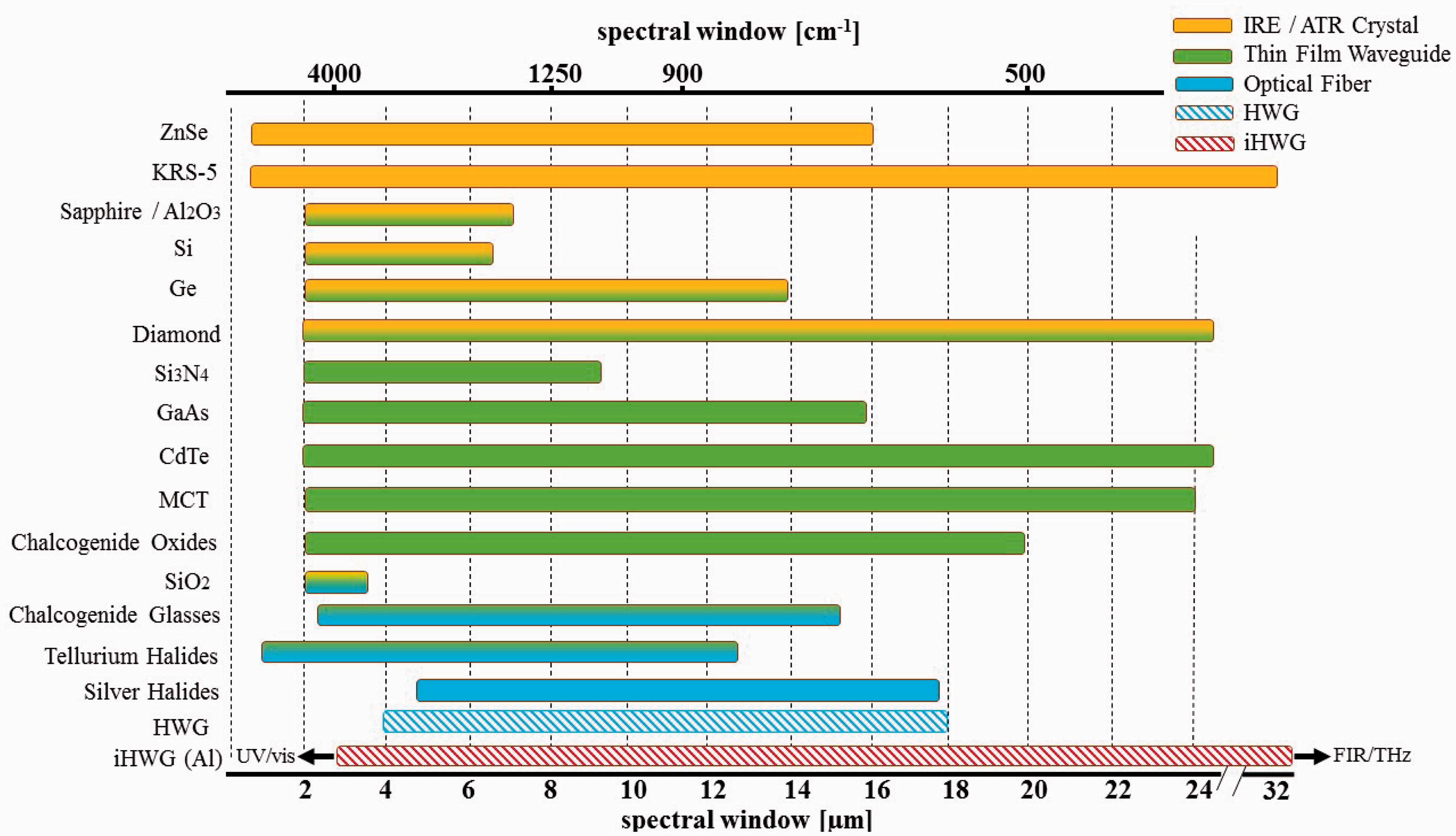
Given their MIR transmission window, it is evident why thallium bromo-iodide (albeit nowadays rarely used due to toxicity of the material), zinc selenide, silicon, and germanium are among the most commonly used IRE materials, and in particular among commercially available IR-ATR laboratory accessories. However, besides the accessible spectral window, material parameters including the refractive index, the resulting evanescent field intensity, and potential propagation losses when using extended waveguide geometries have to be taken into account. The most prevalent MIR waveguide materials currently used in evanescent field spectroscopy are color-coded in Figure 1 according to their typical application either as conventional IRE mostly in combination with FT-IR-based spectroscopy (yellow), as optical fiber in fiber optic evanescent field spectroscopy and sensing (FEWS; blue), as thin-film and/or on-chip waveguide material (green), as hollow-core optical fiber (dashed blue), or as “substrate integrated hollow waveguide (iHWG)” (i.e., fabricated within an aluminum substrate) with some materials occurring in two or more representations. Integrated hollow waveguides were most recently introduced by the group of Mizaikoff, 34 featuring radiation-reflective hollow waveguide channels enabling transmission from the ultraviolet–visible (UV-Vis) to the FIR-THz regime.
Mid-Infrared Detectors
Probably the most commonly applied detector technology in MIR spectroscopy and sensing utilizes room-temperature, thermoelectrically cooled, or liquid nitrogen cooled (increasing order of detectivity) photoconductive semi-conductor detectors comprising detector materials such as indium antimonide (InSb), mercury-cadmium telluride (HgCdTe; MCT), and the like.35–37 Alternatively, thermal or pyroelectric detectors are of current interest as they are usually significantly cheaper, operated without cooling, provide a spectral response over a possibly broad MIR wavelength band, and may readily be miniaturized.38,39 Adopting the strategy used for QCLs, the same quantum heterostructures may in fact be used as so-called quantum cascade detectors (QCDs) operated without applying a bias voltage 40 which enables further miniaturization and integration of MIR sensing platforms. 41 Quantum cascade detectors are therefore interesting alternatives serving as a photovoltaic version of quantum well IR photodetectors.42,43 Given the fact that QCDs are passive devices only generating a response signal by propagating incident photons via cascading quantum wells, a significantly reduced power budget of the final sensor system is anticipated.
Focus on Mid-Infrared Waveguides: Fundamentals and Classification
Fundamentals of Evanescent Field Spectroscopy and Sensing
Infrared attenuated total reflection spectroscopy is nowadays considered a routine measurement technique when analyzing strongly absorbing films, pastes, gels, powders, and liquids taking advantage of radiation leaking from the waveguide into the adjacent sample environment (a.k.a. evanescent field) upon total internal reflection at the waveguide–sample interface. Total internal reflection occurs if light is reflected at an incidence angle exceeding the critical angle (θ
c
= sin–1(n2/n1), i.e., Snell’s law) at the interface between a high-refractive-index (n1 or nwg) waveguiding element and a low(er)-refractive-index (n2 or nc) cladding, environment. or sample matrix.
44
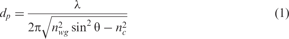
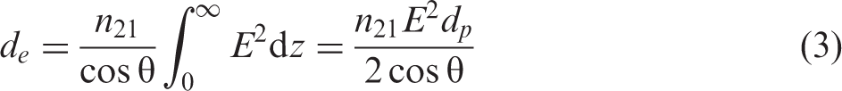
The leaky component of the electromagnetic field (hereon referred to as “evanescent field”) penetrates into the adjacent medium with an exponentially decaying field intensity characterized as the so-called penetration depth (dp). For a given wavelength λ, dp can be approximated as:
44
Molecules present within the evanescent field generated at the waveguide/sample may resonantly interact with this evanescent field interface leading to evanescent field absorption spectrum, a.k.a. ATR spectrum, as a result of the attenuation of the propagating radiation at analyte-specific frequencies. Absorption within the evanescent field essentially follows a Beer–Lambert relationship according to:
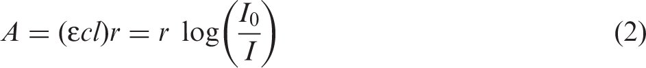


Since usually αde is<1, it may be safely assumed that the absorbance for N reflections approximately equals N-times the absorption of a single reflection.20,45,47 Using such basic geometric considerations when generating an evanescent field, one may readily derive the first generation of MIR waveguides termed “internal reflection elements (IREs)”.
First Generation Mid-Infrared Waveguides: Internal Reflection Elements
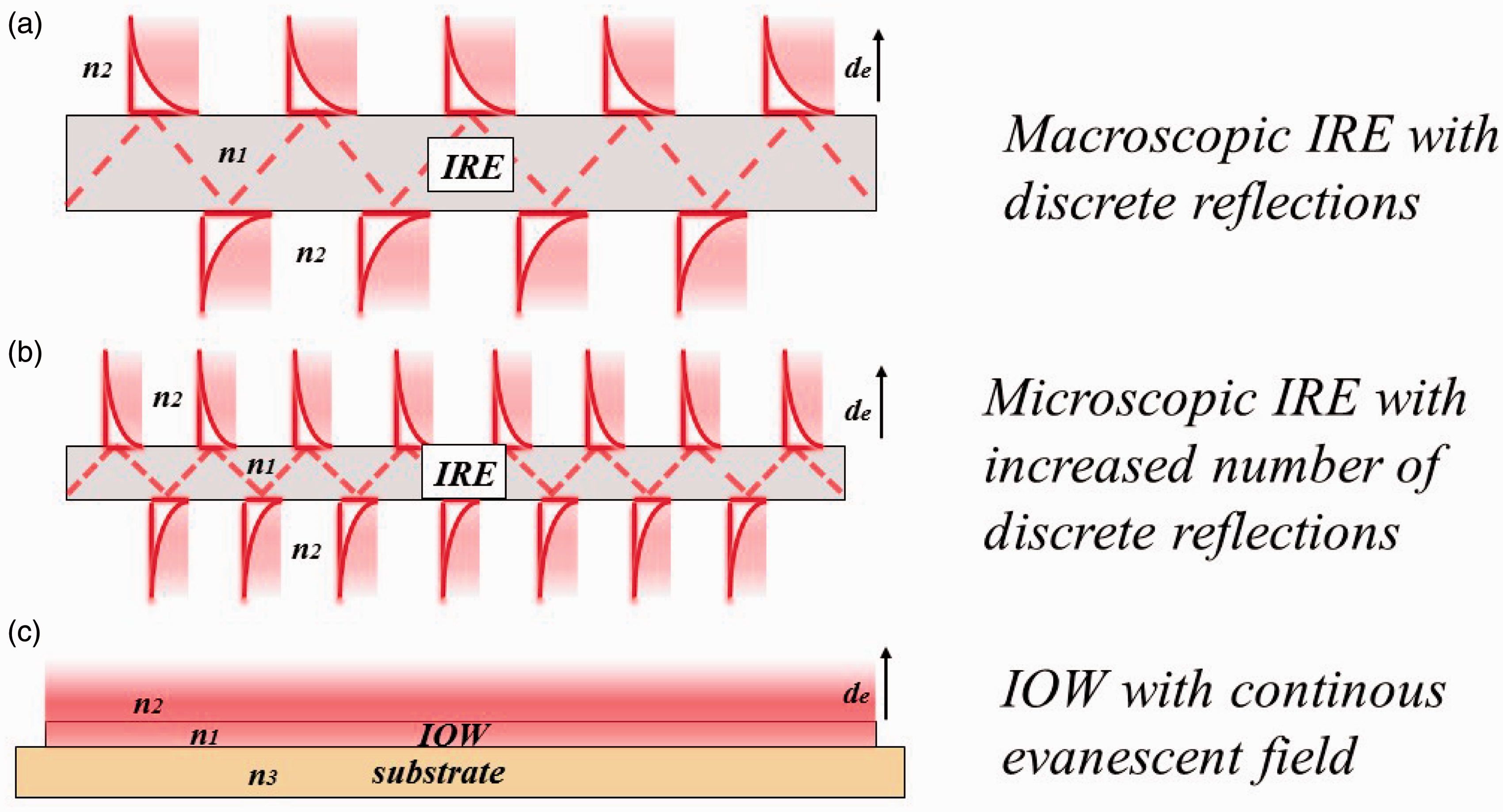
Considering the propagation of radiation inside a waveguide for waveguide dimensions significantly larger than the wavelength at the conditions of IRE conditions (i.e., as is the case for conventional IREs), conventional geometric optics result in the emergence of evanescent field spots at each reflection along the IRE surface (Figure 2).
(Left) Schematic representation of radiation propagation inside and the evanescent field at the surface of an IRE featuring (a) a macroscopic multi-reflection IRE (e.g., trapezoid with 1 mm thickness) and (b) an IRE twice the thickness (2 mm) at the same angle of incidence. Albeit not to scale, the increase in density of evanescent field spots responsible for generating the analytical signal (i.e., absorbance) with decreasing IRE thickness is immediately evident. (Right) Schematic increase in penetration depth and thus intensity of the evanescently guided radiation at similar optical conditions for (c) a germanium IRE with a refractive index of 4.06, and (d) a zinc selenide IRE with a refractive index of 2.44. Note that for clarity the evanescent field is only shown at the upper surface of the IRE.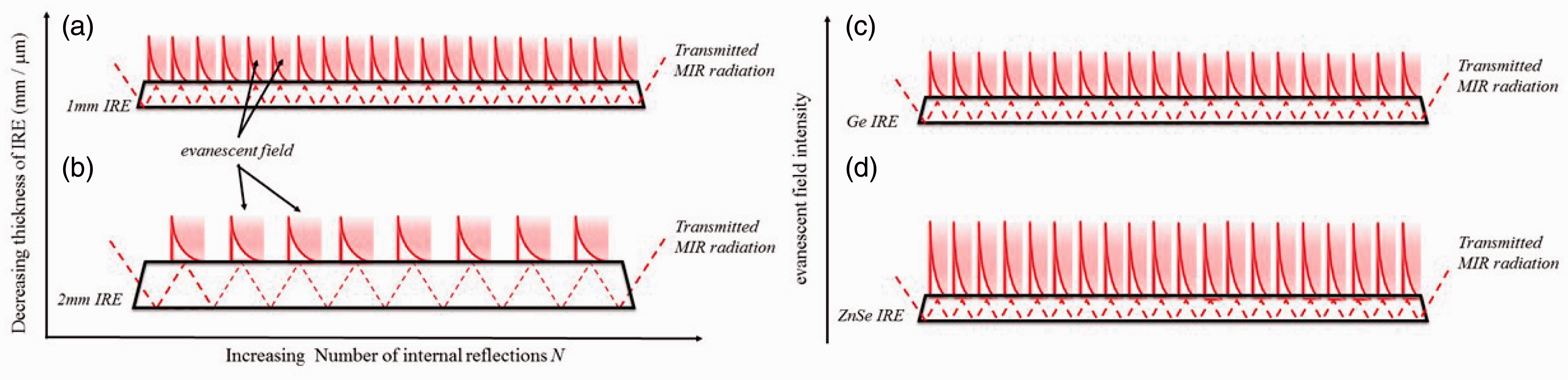
Figure 2 schematically illustrates the influence of the thickness and material choice of the IRE. Considering the IRE thickness (Figure 2a and b), the number of internal reflections scales with the waveguide dimensions for obvious geometric reasons, which should increase the sensitivity of the measurement with decreasing waveguide thickness. However, while reducing the IRE thickness positively affects the sensitivity, the decreasing optical aperture adversely decreases, usually resulting in fewer photons coupled into the IRE; likewise, more internal reflections may lead to increased reflection losses. Hence, the signal-to-noise (S/N) ratio will be negatively affected usually requiring more sensitive detectors for compensation.
Conversely, Figure 2c and d schematically illustrates how the selected IRE material (i.e., its refractive index or, more generally, dielectric constant) may affect the penetration depth and intensity of the evanescent field. Decreasing the refractive index of the waveguide material increases the penetration depth, and thus, increases the interaction volume with molecules at the waveguide–sample interface, which positively affects the SNR during absorption measurements.
In summary, it is immediately evident that optimizing the waveguide structure, dimensions, and geometry (i.e., number of internal reflections), along with the optical properties of the waveguide material (i.e., penetration depth of the evanescent field) are major parameters for maximizing the performance and sensitivity in waveguide-based MIR spectroscopy and sensing concepts.
Second Generation Mid-Infrared Waveguides: Optical Fibers
During the past three decades, fiber optic evanescent wave spectroscopy and sensing schemes have emerged as a viable alternative to conventional IREs in absorption spectroscopy, taking advantage of MIR transparent optical fibers as waveguide and actual sensing element.
48
Evidently, using optical fibers enables extended separation of the actual active sensing interface from the light source and detector, thus facilitating the design of a fiber optic sensor for in-situ experiments. Given the length of optical fibers (i.e., several meters for MIR fibers at acceptable attenuation losses) and their mechanical flexibility, the main advantage versus first generation waveguides is the opportunity of robust light guiding and sensing in remote application scenarios (i.e., “guiding photons to the sample rather than bringing the sample to the spectrometer”). Next to fine-tuning of the fiber thickness, surface, and radiation in-/out-coupling facets, the active sensing region of the fiber (where the fiber serves as evanescent field sensing element interacting with sample molecules upon immersion) may be tailored. For example, the interaction length may be significantly extended versus conventional IREs (e.g., “spiraling” of the fiber; see Figure 3b) or the fiber geometry may be designed for maximizing the number of internal reflections within the sample interaction length by symetrically tapering (e.g., etching, pulling, or thinning a cylindrical segment) or flattening the fiber core (see Figure 3c). Furthermore, due to its rotational symmetry (Figure 3a), usually the entire evanescent field surrounding the fiber is used for generating the absorption signal as the fiber may readily be sealed as a suspended IRE within a flow-through cell, whereas conventional IREs usually utilize only one side of the waveguide for the actual measurement (i.e., with the exception of macroscopic ATR rods).
Schematic examples for fiber optic evanescent field sensing concepts. (a) Vector representation of radiation propagation inside a fiber optic waveguide. Here, the evanescent field is generated along the propagation vector throughout the fiber core (in all three dimensions). (b) Remote sensing via FEWS with MIR radiation propagating, e.g., along core-clad optical fibers generating an analytically useful evanescent field (i.e., accessible by sample molecules) only along the unclad active sensing region at a distance from light source or spectrometer and detector. (c) Tapering or flattening of the fiber core within the active sensing region leads to an increased number of internal reflections as a consequence of the reduced waveguide thickness and the tapering angle ω. Schematic representation of evanescent wave/field and radiation propagation with decreasing thickness of the IRE (a, b) leading to integrated optical waveguides (IOW) providing a continuous evanescent field leaking into the adjacent environment (c).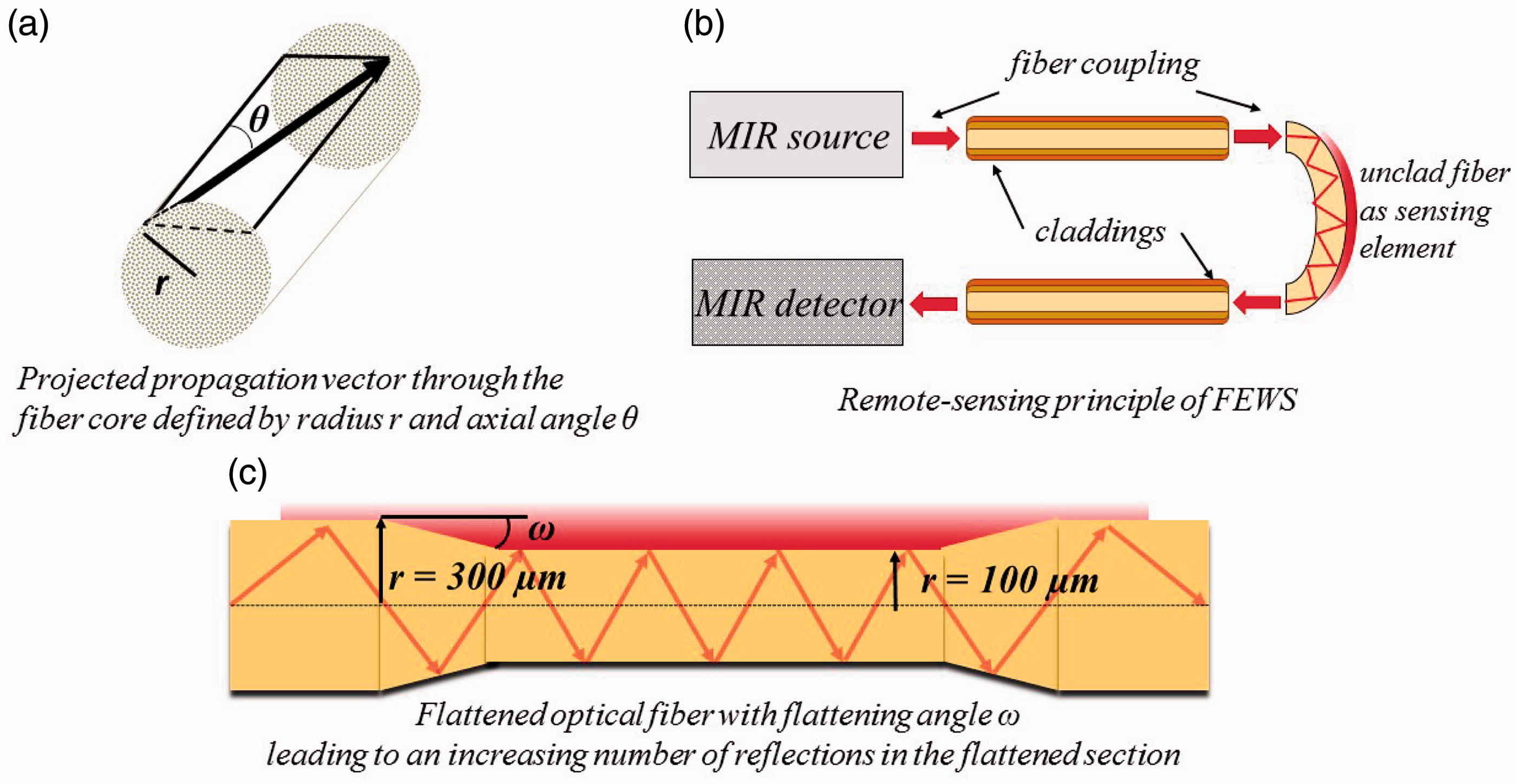
A variety of theoretical models based on simple geometric optics or advanced electromagnetic field theory have been used for describing radiation propagation along fiber optic waveguide structures in great detail. 49 The advances of FEWS in terms of portability and the potential for remote sensing applications constitutes the main breakthrough of fiber optic-based spectroscopic sensors versus the application of conventional IRE-based devices with applications ranging from determining chemical reaction rates, 50 to gas detection 51 and biosensors. 52 However, to date such transducers remain predominantly coupled to commonly applied FT-IR spectrometer systems.
In order to improve the achievable sensitivity, tapering and flattening of fiber optic waveguides has been applied, albeit limited to a thickness of usually few tens of micrometers of the tapered active sensing element, as the thinned section is of increasing mechanical fragility. Hence, real-world application scenarios usually abstain from using tapered fibers in chem/bio sensing. Likewise, while in principle possible, it is of little practical value to taper fibers to a thickness on the order of magnitude of the wavelength (i.e., <20 μm) for achieving single-mode radiation propagation behavior. Consequently, the advent of advanced MIR laser light sources such as QCLs and ICLs demanded a third generation of MIR waveguides: thin-film planar waveguiding structures.
Third Generation Mid-Infrared Waveguides: Thin-Film Waveguides
As discussed so far, the thickness of most conventionally applied waveguides significantly exceeds the order of magnitude of the propagated wavelength. As the number of reflections is inversely proportional to the thickness of the IRE, thinning the waveguide to dimensions corresponding to the wavelength increases the effective absorption path length until ultimately a uniform evanescent field is obtained extending along the surface of such core-only waveguide structures, which may lead to substantial sensitivity enhancements. 53
Since light propagation within such thin-film waveguides may no longer be adequately described via a series of internal reflections, the generated continuous evanescent fields are represented via more sophisticated models based on wave analysis. Waveguides realized at these dimensions are commonly referred to as thin-film waveguides or integrated optical waveguides (IOWs).
Hence, without being discussed here in detail, rather focusing on the analytical and applied spectroscopic aspects, parameters such as mode confinement, lateral distribution of the radiation in various modes (i.e., TE, TM, etc.), etc. lead to the fact that IOWs facilitate significant increases enhancements of the evanescently guided field intensity and penetration depth, thereby enabling specifically tailoring waveguide structures to selected applications. However, it should be noted that most commonly such thin-film waveguide structures are deposited at and mechanically supported by suitable (i.e., refractive index matched) substrate materials, with the possible exception of sufficiently robust free-standing thin-film diamond waveguides, thus providing only one surface of the waveguide for active sensing purposes.
Recent Trends and Selected Applications
Given that extensive literature has been published on conventional IREs and MIR transparent optical fibers, and applications thereof,3,20 this review focuses predominantly on recent trends in both waveguide technology and applications that have emerged during the last decade. Most condensed materials by nature of their inherent structure reveal vibrational transitions limiting their MIR transparency. Hence, semi-conductors of different compositions appear most suitable for providing sufficient transmittance in the electromagnetic spectrum of interest and for establishing tailorable waveguiding platforms. Among the fabrication techniques, drawing or growing optical fibers next to chemical vapor deposition (CVD) for planar waveguide structures (i.e., IREs) remain among the most commonly applied fabrication processes for MIR transparent waveguides. 54
With the emergence of third generation thin-film waveguides and integrated MIR optics, techniques initially developed predominantly for silicon-based microfabrication are increasingly being adopted for the development of miniaturized MIR sensing platforms (a.k.a. MIR on-chip device technology). Processing techniques including UV photolithography, electron beam patterning, (hot) embossing, and so on facilitate rapid and straightforward processing even of sophisticated optical device designs. 55 Simple IOWs comprising strip or rib waveguide structures of a higher refractive index n1, most commonly semi-conductor, material are locally deposited on top of a suitable substrate (i.e., usually wafer-based substrates with any number of strain and/or refractive index matching additional interface layers) with a lower refractive index n2. Alternatively, previously deposited waveguide films are etched after lithographic structuring (e.g., wet etching, reactive ion etching, etc.) readily creating three-dimensional linear waveguide structures or more sophisticated optical geometries (e.g., ring-, disc-, or racetrack-shaped resonators) with precise control on the desired dimensions.
Evidently, current trends in waveguide-based MIR applications increasingly take advantage of waveguides as an active transducer, rather than merely serving as a radiation propagation conduit. From an analytical spectroscopy perspective, this is an essential—if not the most essential—function, as the transducer plays the major role within optical sensor systems in generating the actual analytical signal by ensuring reproducible intimate interaction between photons and sample constituents (i.e., conversion of chemical, biochemical, or biological processes or recognition events into changes of optical properties). While nowadays optical chemosensors increasingly take advantage of the distinctive molecular signatures generated in the MIR regime, only few representative examples of optical biosensors operating in the MIR have been published. This may be attributed to the fact that, with few recent exceptions, the sensitivity of first generation waveguides (i.e., conventional IREs) and even second generation fiber optic-based liquid phase MIR sensors remains insufficient for detecting: (1) small quantities of relevant biomolecules such as, for example, proteins or DNA; and (2) in appreciable small volumes (i.e., microliter regime). In contrast, limited sensitivity of MIR chemosensors is readily mitigated by using, for example, solid phase enrichment schemes via immobilization of appropriate polymer, sol-gel, or similar membranes directly at the waveguide surface acting as in-situ enrichment membranes; a strategy applicable for conventional IREs, fiber optic transducers, and IOWs. Thereby, detection levels in the parts per billion (i.e., μg/L) concentration range have been realized in a true chemical physico-chemical sensing format (i.e., diffusion of analyte molecules into and out the solid phase membrane in lieu of chemical reactions). Using such membranes, IR-ATR-based chemosensors have been developed serving for environmental contaminant monitoring,32,56 in pollutant analysis,11,57,58 and even in microbiological applications,
59
as exemplarily illustrated for detection of volatile organic components (VOCs) towards dissolved oil fingerprinting in aqueous/marine environments (Figure 5).
(Top left) Schematic of IR-ATR system comprising a macroscopic ZnSe IRE coated with a polymeric enrichment membrane for detecting organic pollutants in marine environments (i.e., dissolved oil fingerprinting via characteristic VOC patterns dissolved in the aqueous phase). (Bottom left) Characteristic absorption patterns of dissolved hydrocarbons detected via IR-ATR evanescent field absorption spectroscopy after enrichment within a suitable polymer membrane. (Right) Analytical response of a polymer-coated diamond IRE in aqueous solution at a contaminant concentration of 50 ppm (p-xylene). Adopted and reprinted with permission from ACS Publishing, 2014/2015.32,57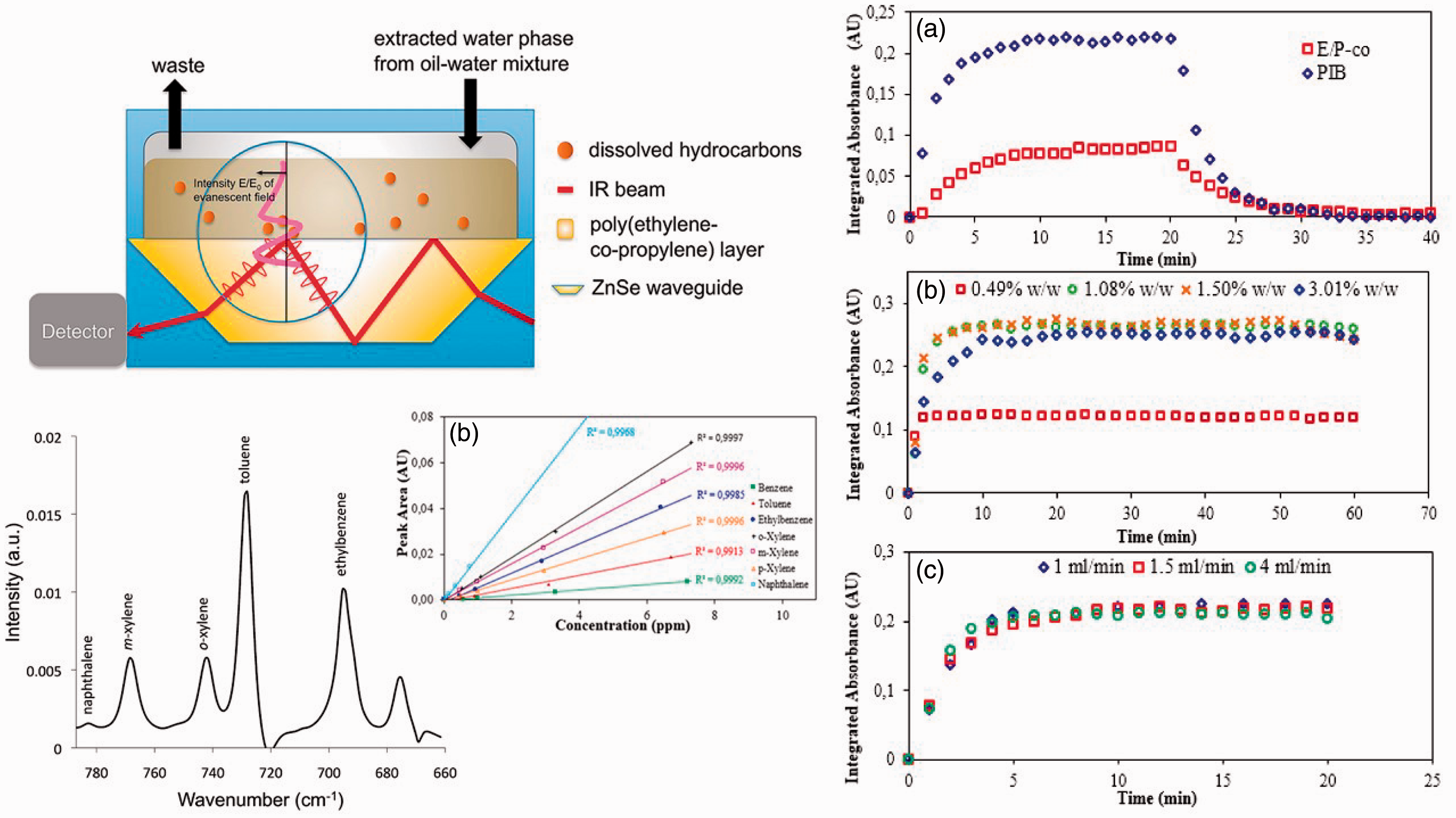
After optimization, the application of conventional IR-ATR techniques using membrane-coated macroscopic IREs revealing characteristic concentration patterns of dissolved VOC fractions assignable to different oil contaminations at trace levels has been shown.32,56 Obtaining such low detection limits for relevant pollutants supports the potential of MIR sensors for in-situ analyses and monitoring purposes. Nevertheless, in-field applications require a significant scaling of involved instrumentation for facilitating, for example, on-ship studies. Given ongoing progress in miniaturized MIR waveguide technology, light sources, and detectors, it is anticipated that waveguide-based IR sensing systems for in-situ and in-field monitoring (e.g., in marine environments) are within reach.
As a consequence, more compact MIR sensor systems utilizing ATR sensing concepts are predominantly focusing on miniaturizing the actual MIR transducer as well as the entire instrument, yet maintaining the sensitivity via improved chem/bio recognition architectures. Giammarco et al. proposed a method combining an innovative multi-layered coating with ATR waveguide technology.
60
The established enrichment polymer film had a thickness of only 27 nm, and was capable of extracting a variety of constituents for determination via the evanescent field emanating at an IRE surface (Figure 6).
(a) Schematic illustrating the interaction of a multi-layered enrichment coating with various analytes. (b) Schematic of the micro-disc-on-chip system (left), and top view image of a micro-disc resonator in a pulley-coupler configuration (right). (c) Infrared attenuated total reflection spectra of various analyte vapors detected using the multi-layered enrichment coating deposited at a Si crystal waveguide surface. Reprinted with permission from RSC Publishing, 2011.
60
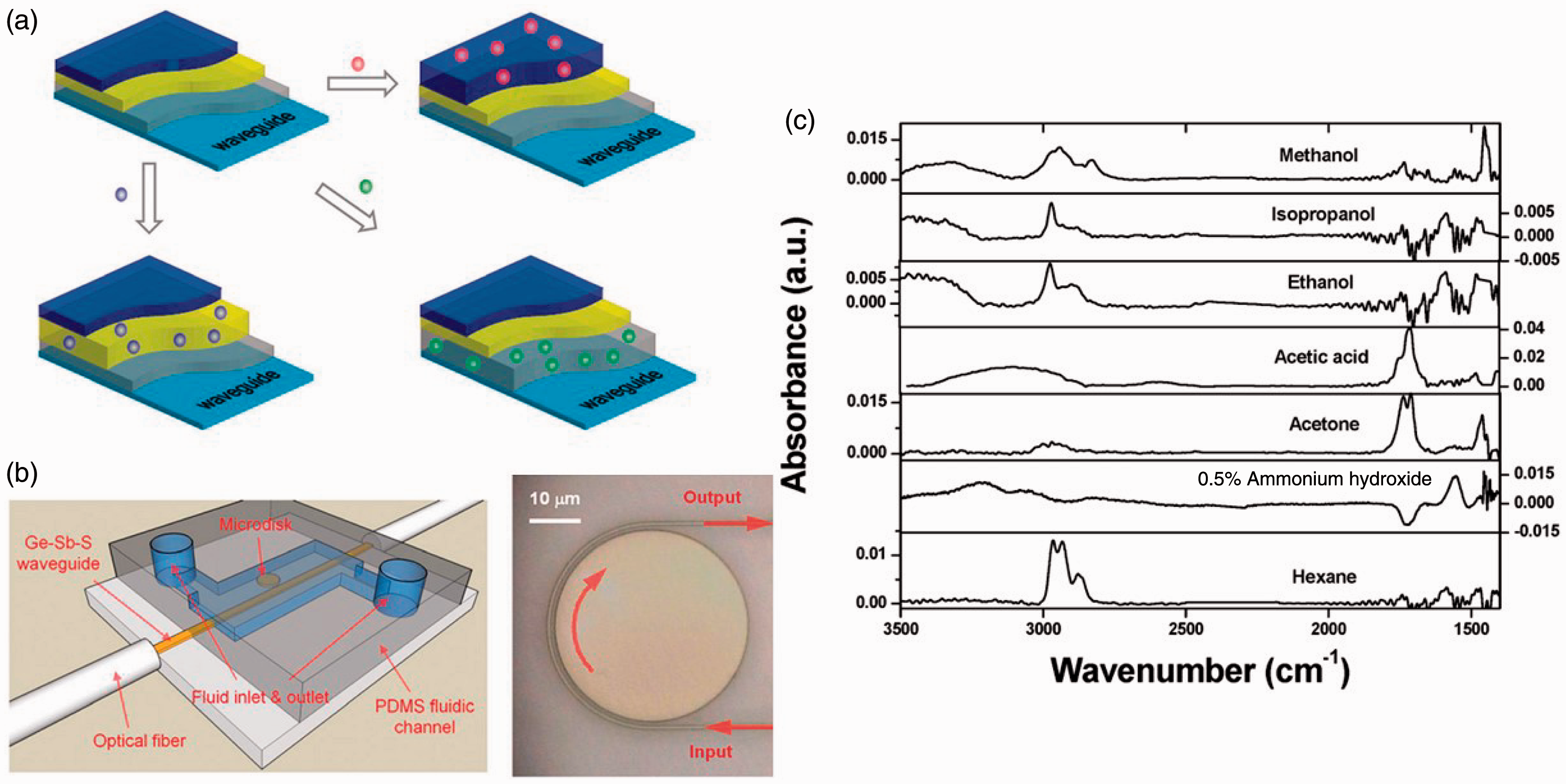
Here, an advanced architecture that comprised a multi-layer nanostructured polymer film was immobilized at the surface of the MIR transducer, which represents a straightforward and robust approach for the fabrication of nanocoatings at IR-ATR waveguide surfaces. Due to the multi-layer nature of the membrane, a variety of components may be enriched from aqueous and vapor phase samples directly at the waveguide surface facilitating analysis via evanescent field absorption.
In FEWS, the group of Katzir and Raichlin is among the pioneers of evanescent wave spectroscopy using silver halide (AgClBr in various compositions) optical fibers. These polycrystalline fibers are mechanically flexible and malleable materials with a wide MIR transmission window and therefore lend themselves for various tapering procedures. For example, a central section of the fiber may be flattened to a thickness of approximately 100 μm at a length of 1–5 cm width of several millimeters.
61
By adusting the length and angle of the section leading into the flat tapered segment, the angle of incidence during propagation of the radiation within the fiber core may be tailored such that maximum penetration depth and number of reflections is achieved, thus maximizing the achievable analytical sensitivity of such fiber optic transducers. Raichlin et al. recently reported evanescent wave spectroscopy using flattened fibers for detecting micrograms of insoluble hormones and explosives (Figure 7). Following their increasing usage in medication, contraceptives, agriculture, and so on, hormones are considered among the most relevant emerging microcontaminants of environmental concern, due to their adverse effects on animal and human health (e.g., endocrine disrupting effects, etc.). Forensic applications
61
of MIR FEWS are increasingly adopted via detecting explosive residues at crime scenes and for implementing potential screening strategies in airport security.
(a) Exemplary spectrum of β-estradiol obtained via a silver halide fiber optic sensor system. (b) Spectrum of dry powder β-estradiol determined via a commercial IR-ATR (i.e., diamond IRE) system and a FT-IR spectrometer. The dry powder was pressed onto the prism-shaped diamond ATR element. (c) Fiber optic evanescent wave measurement of an explosive (TNT).
61
Reprinted with permission from Elsevier, 2014.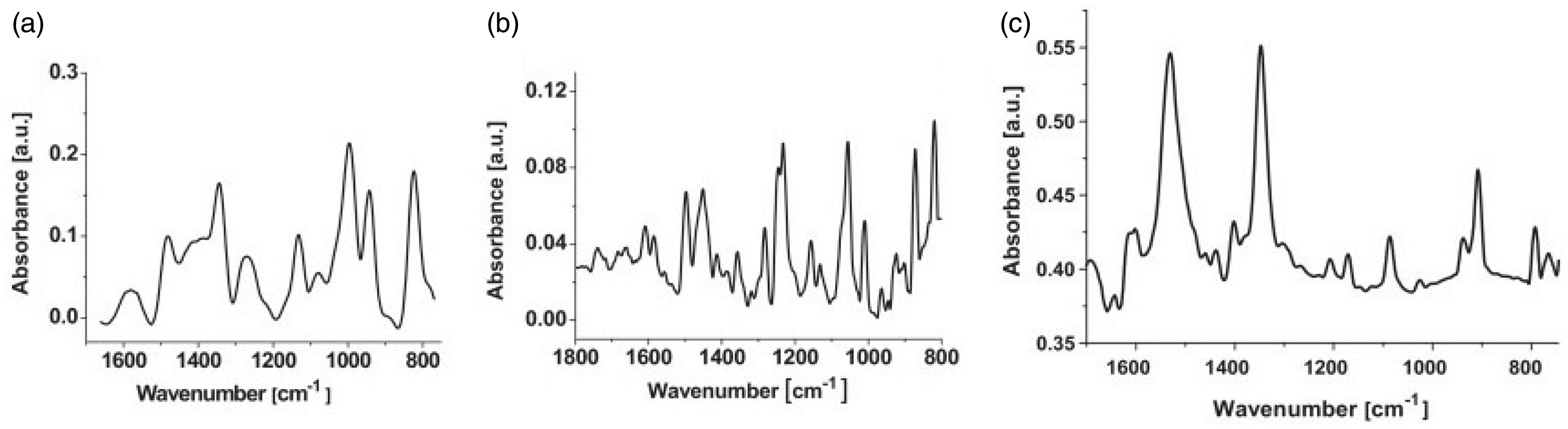
For biological applications, the Pleshko group recently reported a fiber optic method quantifying collagen and elastin at an in-vitro model of extracellular matrix degradation processes in aorta samples.
62
The extracellular matrix is a key component and regulator within a wide variety of biological tissues. The aorta is the major blood vessel responsible for blood circulation, and aortic diseases have emerged among the leading causes of death in developed countries. A custom-made optical fiber probe based on a silver halide sampling tip mounted at the end of a 1m long silver halide fiber was connected to a commercial spectrometer, thereby generating an ATR sampling tip with a length of 15 cm and a diameter of 3 mm, as illustrated in Figure 8.
(Top left) (a, b) Aorta samples prepared as open rings of a few centimeters in length. (c) Custom fiber optic sampling tip for IR-ATR data collection next to a US quarter dollar coin for size comparison. (d) Actual data collection from an aorta sample. (Bottom left) Elastin and collagen content within aorta samples at different anatomical locations. (Right) Average spectra of samples with low, medium, and high elastin content. (a) Reference spectra of collagen–elastin recorded via conventional transmission spectroscopy. (c–e) Fiber optic spectra of collagen-elastine and their second derivatives (b, d, f).
62
Reprinted with permission from RSC Publishing, 2014.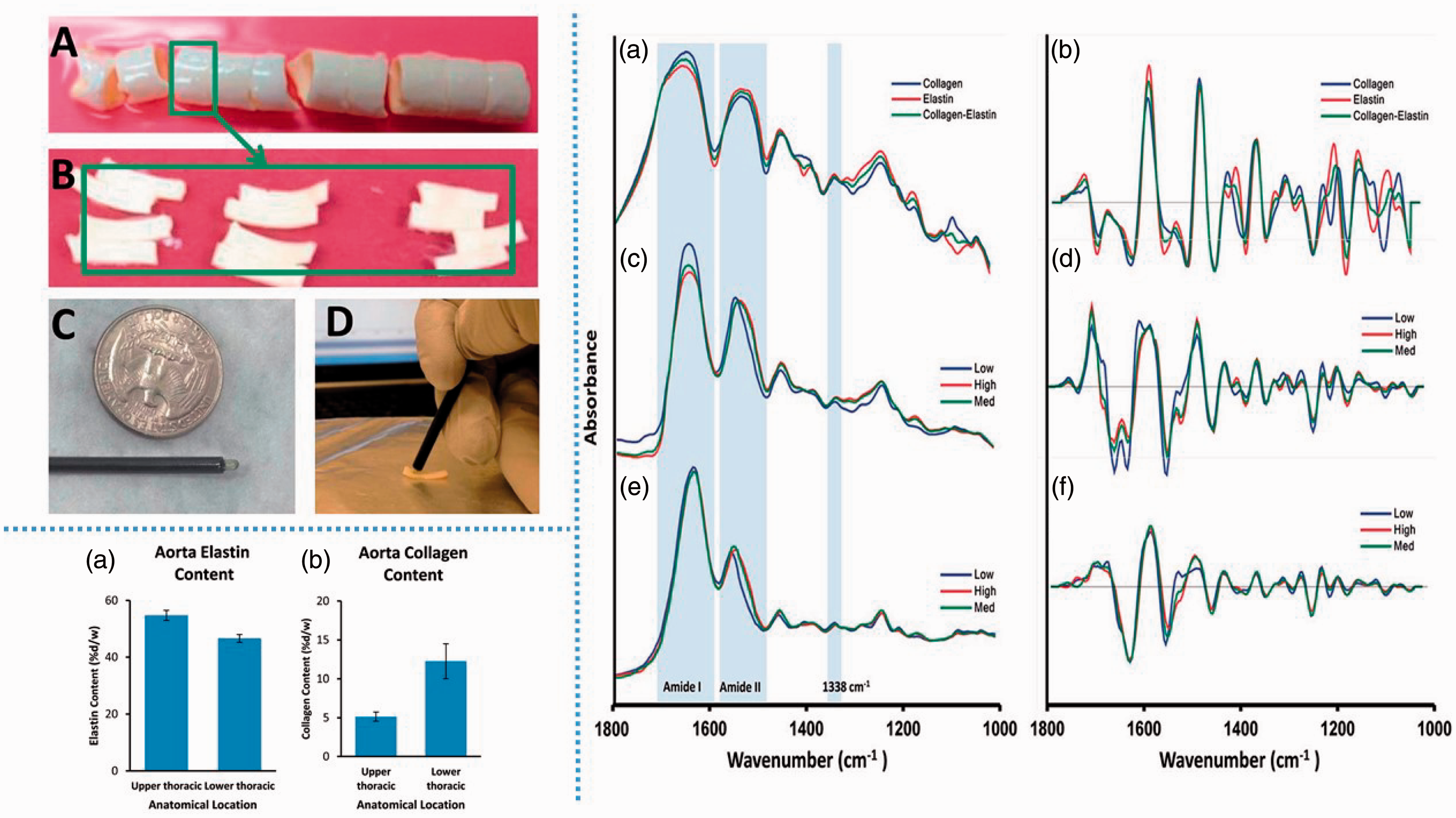
This methodology enabling identifying collagen or elastin in aortic tissue is an interesting and promising approach for studying changes of extracellular matrices in different aortic diseases with minimal preparation compared to common histological or immunohistochemical methods. In addition, a multivariate calibration model was presented for automatically quantifying elastin within intact aortic tissue via the MIR fiber optic probe.
Such studies clearly illustrate that, besides the development of advanced thin-film MIR waveguide technologies, MIR transparent optical fibers remain of substantial utility for identifying and quantifying organic, inorganic, or biological constituents and their chemical properties. Hence, FEWS methods remain a viable alternative in IR-ATR spectroscopy and sensing due to usually straightforward optical configurations, reduced cost versus conventional IREs, a minimal requirement on sample preparation and processing. In addition, small sample quantities and areas may be addressed, which is of particular interest in biomedical applications, whereas the sensitivity of such fiber optic probes lends itself to applications in environmental protection/monitoring, drug enforcement, and homeland safety/security.
Among the already limited set of MIR transmitting materials applicable for fabricating fiber optic waveguides, there is an even more limited selection of materials useful for establishing on-chip thin-film waveguide structures. In addition, using semi-conductor materials for chem/bio sensors has to consider their chemical robustness in terms of, for example, high (or low) pH values, elevated temperatures, mechanical stress, and so on. Yet, the emergence of advanced QCL and ICL light sources demands for frequency-matched waveguide layers and structures for fully unlocking the potential of these almost ideal light sources.
Therefore, besides the rather excellent transparency throughout a broad wavelength window, diamond has emerged as a most interesting option also for MIR waveguide structures. Nowadays, diamond fabrication is predominantly performed via chemical vapor deposition (CVD)
63
at low-pressure–high-temperature conditions (LPHT), because of the metastable transition of diamond to graphite at high temperatures. However, LPHT requires expensive equipment and experience in the fabrication process, lacks in reproducibility when processing of large numbers of samples. As a result, LPHT annealing remains a unique technique available only at few laboratories and companies for research and small-scale production.
64
Yet, methods for thermally etching diamond have been reported in recent years,
65
which facilitate processing of miniaturized diamond structures. An example of these established free-standing diamond strip waveguides (DSWGs) and their potential utility for chemical sensing is illustrated in Figure 9.
(Left) Diamond strip waveguides (DSWGs) grown at a passivated silicon wafer substrate. (a) Microfabricated free-standing diamond waveguides with a series of strip widths (100−500 μm) compared in size to a Euro one cent coin. (b) Scanning electron microscopy image at the in/out-coupling end facet for a 100-μm wide waveguide with a thickness of 14 μm representing the actual free-standing waveguiding strip . (c) Schematic of the thin-film diamond waveguide structure on top of the substrate layers. (Right) Infrared absorption spectra of anisaldehyde and chemical response of the sensor recorded with a tunable QCL after deposition at the surface of a thin-film diamond waveguide and comparison of the IR-ATR spectrum recorded using a conventional FT-IR spectrometer averaging 200 spectra is shown. Reprinted with permission from ACS Publishing, 2014.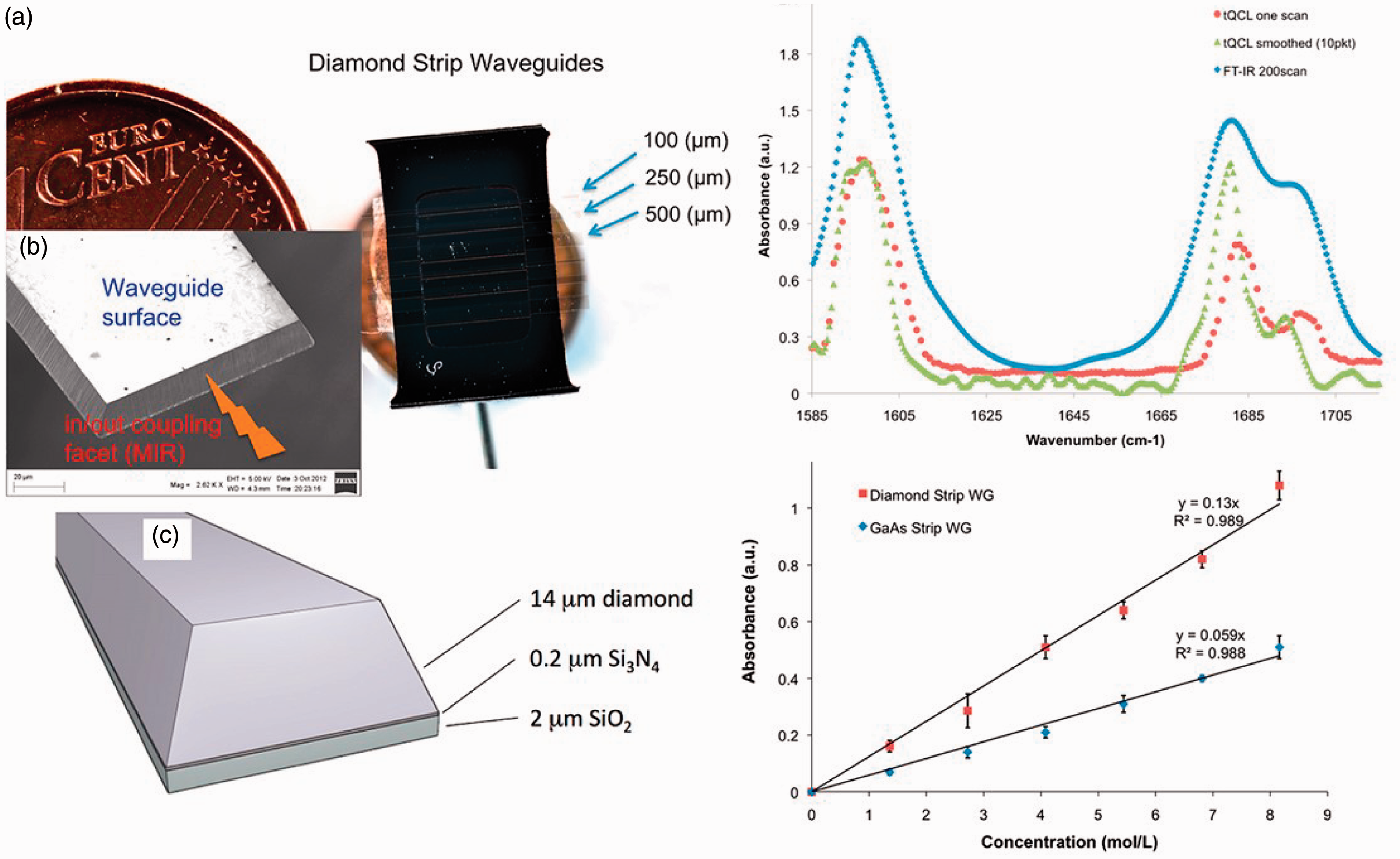
This sensing application clearly demonstrates the potential optical/analytical performance for evanescent field sensing using diamond as an advanced waveguiding layer, which might be among the key developments for enabling highly miniaturized MIR optical sensing platforms in combination with appropriate tunable QCLs or ICLs. Considering the generally already achieved level of miniaturization/integration of other wavelength optical devices (i.e., in the NIR and UV-Vis wavelength regime), the opportunities for MIR chemical sensors/biosensors upon appropriate miniaturization are immediately evident towards molecularly selective MIR diagnostics. Following this route, further structured waveguides offer opportunities for further miniaturizing and integrating optical components into possibly small devices, yet offering comparable results in terms of analytical sensitivity and reproducibility versus laboratory-based spectroscopic MIR analyzer systems. For example, a three-times higher SNR value was shown by the research group of Mizaikoff 66 using diamond strip waveguides combined with QCL light sources versus commercial FT-IR spectrometers. Because of the outstanding robustness of diamond even at harsh environmental conditions, as well as its intrinsic biocompatibility, diamond has excellent prospects to emerge as the most interesting material for next-generation on-chip MIR chem/bio sensors combined with QCL and ICL light source technologies.
Another promising group of materials for thin-film-based MIR sensors are the chalcogenides, i.e., mixtures containing S, Se, As, and Te, which are commonly known for their broad optical transparency and high refractive index in optical fiber technology (i.e., second generation waveguides). Several chalcogenide material compositions are also being applied for fabricating thin-film waveguides taking advantage of the high refractive index contrast between the chalcogenide layer and a suitable substrate. For example, using GeTe4 as a waveguiding core layer at a ZnSe substrate with respective refractive indices of 3.34 and 2.43 (at 3.5 μm), a suitable optical density contrast can be generated between core and substrate, thus increasing the intensity of the evanescent field yielding high surface sensitivity at the waveguide/analyte interface. Using these materials, channel waveguide structures have been realized in the 2.5–3.7 and 6.4–7.5 μm spectral region.
67
The research group of Mittal et al. recently reported a convenient fabrication method for such waveguide structures using sputtering and lift-off techniques to realize GeTe4 waveguides on ZnSe substrates later applied in evanescent field sensing (Figure 10).
(a) SEM image of a cleaved cross-section of GeTe4 film as deposited ; (b) top view of GeTe4 channels fabricated by lift-off techniques; (c) X-ray diffraction pattern and atomic force microscopy image of the ZnSe substrate and the GeTe4 films. (d) Distal coupling facet of the waveguide cut by ductile dicing.
67
Reprinted with permission from The Optical Society Publishing, 2015.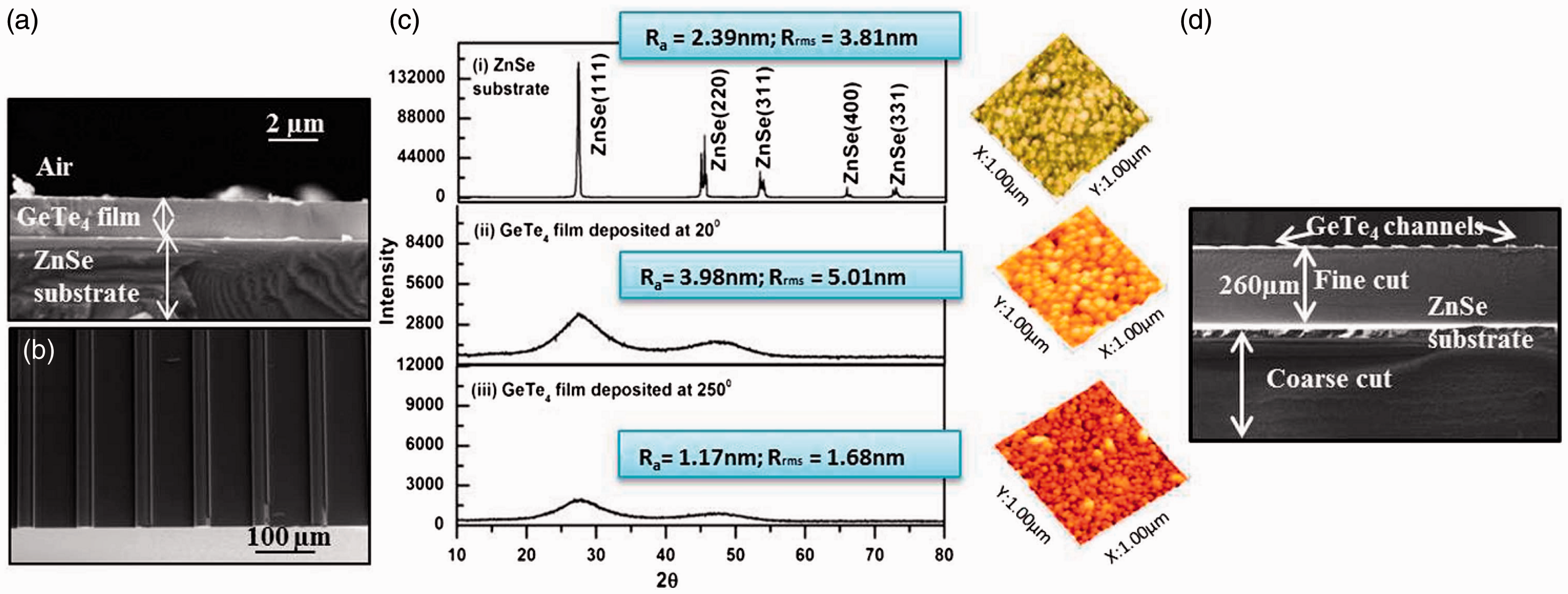
The reported thin-film waveguides were found to be amorphous in nature with an average surface roughness <4 nm providing MIR transparency in the spectral range of 2–20 μm, while actual waveguiding was demonstrated in the 2.5–3.7 μm and 6.4–7.5 μm regime. While single-mode behavior is desired for most biochemical sensing experiments, the reported GeTe4 channels revealed multimode behavior for the given wavelength ranges. However, the authors state that a multimode waveguide design was selected on purpose in order to establish waveguiding also at longer wavelengths (i.e., up to 12 μm) ensuring sufficient coupling efficiency via commercially available single-mode fibers. In future, the applied materials and fabrication techniques may readily be adapted to achieve single-mode behavior. 67 Incidentally, the combination of thin-film channel waveguides and MIR optical fibers as coupling elements also highlights that these waveguide technologies are not mutually exclusive, but may even be combined to the advantage of the selected application scenario.
Conclusions and Future Perspectives
Classifying MIR waveguide technologies into three generations facilitates documenting the evolution and progress in waveguide technology towards compact, robust, and portable MIR analyzer systems and sensors. The coexistence of these waveguide technologies—now and in future—is certainly a result of the fact that broadband emitters (e.g., as used in conventional FT-IR spectrometers) as well as highly collimated laser light sources (e.g., QCLs, ICLs) enable and facilitate complementary measurement scenarios, and will therefore continue to be developed in parallel rather than replacing each other. Hence, it is anticipated that IR-ATR measurements based on conventional macroscopic IREs will remain prevalent next to thin-film waveguide-based sensing systems addressing analyses in minute sample volumes and at exceptionally low concentrations. Clearly, innovative optical approaches and advancements in integrated optics and photonics will lead to further miniaturized, more versatile, and ideally, but not necessarily, to more efficient and sensitive MIR spectroscopic, sensing, and diagnostic platforms operated at in-field conditions and with trace-to-ultratrace detection limits.
Although the major breakthrough in MIR sensor technology during the past two decades is certainly attributed to the introduction of advanced laser light sources including QCLs and ICLs, it is the actual development of matching waveguide technologies serving as MIR transducers that has been the major driving force towards the analytical applicability of advanced IR sensors and measurement systems. With the recent emergence of on-chip semi-conductor waveguides, the path towards integrated MIR photonic systems (i.e., “IR-lab-on-a-chip” systems) is evidently paved and promises a wide variety of innovative label-free sensing and assay concepts. Finally, with the introduction of more sophisticated optical structures for on-chip waveguides and waveguide-linked technologies including optical resonators, optical couplers, and optical amplifiers along with increasingly complex chem/bio recognition schemes, it is clearly evident that with the advancements discussed herein we are only seeing the beginning of an entire generation of MIR chem/bio sensing and assay devices that will continue to push the envelope in terms of size, cost, and sensitivity.
Footnotes
Acknowledgments
Part of the work herein was performed under the auspices of the U.S. Department of Energy by Lawrence Livermore National Laboratory (LLNL) under Contract DE-AC52-07NA27344. Last but not least, Professor Peter Griffiths (University of Idaho) is thanked for fruitful discussions during preparation of this focal point article.
Conflict of Interest
The authors report there are no conflicts of interest.
Funding
The authors acknowledge support of the waveguide developments at IABC discussed herein by the following projects: European Union’s Seventh Framework Programme managed by REA Research Executive Agency ![]() (FP7/2007-2013) under grant agreement no. 314018 FP7-SME-2012-SME (MYCOSPEC), no. 614002 FP7-Ocean-2013 (SCHeMA), and no. 645758 MSCA-RISE-2014 (TROPSENSE); the Kompetenznetz Funktionelle Nanostrukturen, Baden Wuerttemberg, Germany; the CSIRO Energy Flagship (WA) and the National Geosequestration Laboratory (NGL), Australia; the Center for Integrated Quantum Science and Technology (IQST) at Univ. Ulm/Univ. Stuttgart; the project APOSEMA by the German BMBF/VDI within the M-Era.net program; the International Graduate School in Molecular Medicine Ulm; the Alexander von Humboldt Foundation.
(FP7/2007-2013) under grant agreement no. 314018 FP7-SME-2012-SME (MYCOSPEC), no. 614002 FP7-Ocean-2013 (SCHeMA), and no. 645758 MSCA-RISE-2014 (TROPSENSE); the Kompetenznetz Funktionelle Nanostrukturen, Baden Wuerttemberg, Germany; the CSIRO Energy Flagship (WA) and the National Geosequestration Laboratory (NGL), Australia; the Center for Integrated Quantum Science and Technology (IQST) at Univ. Ulm/Univ. Stuttgart; the project APOSEMA by the German BMBF/VDI within the M-Era.net program; the International Graduate School in Molecular Medicine Ulm; the Alexander von Humboldt Foundation.