
Abstract
We present a review of the use of selected nanofabricated thin films to deliver a host of capabilities and insights spanning bioanalytical and biophysical chemistry, materials science, and fundamental molecular-level research. We discuss approaches where thin films have been vital, enabling experimental studies using a variety of optical spectroscopies across the visible and infrared spectral range, electron microscopies, and related techniques such as electron energy loss spectroscopy, X-ray photoelectron spectroscopy, and single molecule sensing. We anchor this broad discussion by highlighting two particularly exciting exemplars: a thin-walled nanofluidic sample cell concept that has advanced the discovery horizons of ultrafast spectroscopy and of electron microscopy investigations of in-liquid samples; and a unique class of thin-film-based nanofluidic devices, designed around a nanopore, with expansive prospects for single molecule sensing. Free-standing, low-stress silicon nitride membranes are a canonical structural element for these applications, and we elucidate the fabrication and resulting features—including mechanical stability, optical properties, X-ray and electron scattering properties, and chemical nature—of this material in this format. We also outline design and performance principles and include a discussion of underlying material preparations and properties suitable for understanding the use of alternative thin-film materials such as graphene.
Keywords
Introduction
A sample support or window should contribute to a measurement only in the desired manner. An ideal cuvette, for example, would define the path length but not affect the optical transmission. In spectroscopic applications, the usual approach is to minimize material absorption by choice of window material.
1
In a charged-particle technique such as transmission electron microscopy (TEM), however, the strong interaction between the interrogating beam and matter places stringent limits on the material composition and thickness of any sample support through which the beam must pass. Sample-dependent solutions for TEM have included supports with open areas to leave samples unobscured (but unsupported over that opening), and thin carbon and polymer films that minimize signal loss by reducing support thicknesses. There is considerable “art” in the fabrication of many support films:2,3 the adoption of nanofabricated thin films has expanded the library of materials and structures to include thin-film silicon nitride, graphene, and nanostructured variants such as porous silicon, among others.4–15 Both composition and thickness can be tuned in concert to obtain optimal performance. More broadly, new performance capabilities can be engineered (or discovered) when the thin-film sample support or window itself becomes a focus of investigation. Silicon nitride thin-films offer superb mechanical properties—a < 100 nm thick window can withstand over an atmosphere of cross-film pressure differential, for example
16
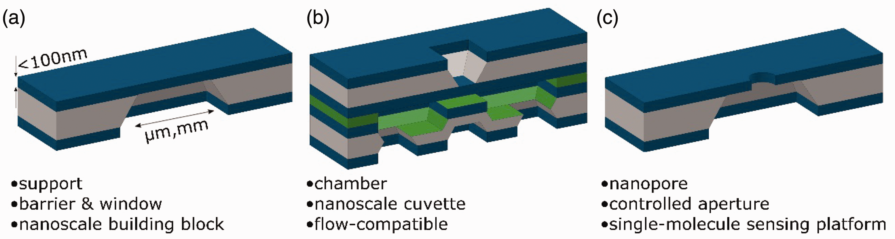
—and this can be exploited to create sample supports and containers that overcome severe challenges such as nonlinear window responses on short timescales in ultrafast spectroscopy.17–19 Thin films with suitable properties and structures can also be used in a more active role in experimental studies: a ∼10 nm diameter channel through a < 100 nm thick thin film—a so-called nanopore—is the basis for a wide range of single molecule sensing and manipulation methods that emerge from the passage of a molecule into, or through, the nanofluidic channel.20–29 Fig. 1 offers two illustrations to illuminate the rich scope of experimental configurations and possibilities using just these two platforms. We will frame our discussion of the interplay between thin-film design—composition and structure—and application by using these two quite different implementations: a sample cell with thin-film windows bracketing a nanofluidic channel; and a nanopore single molecule sensor platform where the robust thin film supports a nanofluidic through-channel. Fig. 2a shows the common structural foundation of the two nanofluidic devices: a free-standing thin silicon nitride film supported by a silicon frame.
16
We will use this canonical construct and material to discuss key design and operating considerations, highlight experimental accomplishments, challenges, and opportunities, and touch on alternative materials and architectures.
(a) A < 100 nm thick layer of liquid and sample (yellow spheres) between two thin windows can be interrogated with a range of optical and particle probes (red and blue beams), in isolation and combination, yielding molecular-level insights over a range of time and length scales. (b) A ∼ 10 nm diameter central nanochannel can be used to detect and entrain single molecules for interrogation by a variety of methods such as electron tunneling (e.g., using transverse electrodes proximal to the pore) and single molecule fluorescence. Molecular coatings (wavy lines at upper right) can tune the performance of nanopores (and other nanofluidic devices) through judiciously chosen terminal functional groups (red curve). Bacteriochlorophyll molecule from Cambridgesoft Perkin Elmer;
30
scaling is not intended to be rigorously representative. (a) The basic < 100 nm-thick SiNx membrane, free-standing over an open aperture in Si can serve as (b) the windows of a nanofluidic cell with additional features such as a wetting layer (green) added through conventional nanofabrication approaches or (c) be used as a single molecule sensor element after formation of a nanochannel through the membrane.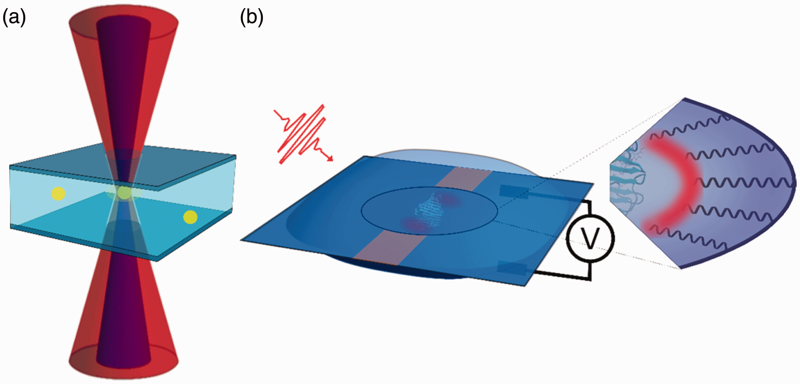
Perhaps the most captivating feature of silicon nitride is its ability to withstand being suspended unsupported, with a film thickness of <100 nm, over millimeter-wide open apertures. A robust, free-standing thin film such as this is a compelling structural component—one that can be further patterned—for use in a host of applications. The freedom from supports is in marked contrast to the usual need for thin carbon film substrates for TEM, for example, to be supported. The success of this unusual configuration hinges on carefully controlling the film stress through the film stoichiometry during fabrication (see below).16,31 Early examples of applications include their use as vacuum chamber windows, to create a wet cell for X-ray microscopy, to protect the source for scanning transmission ion microscopy (STIM) studies in air, to create a sample cell for scanning electron microscopy (SEM) at atmospheric pressure, and to serve as sample substrates for studies using ultrafast spectroscopy, optical microscopy, TEM, and atomic force microscopy (AFM)—and for studies using such techniques in tandem.6–8,16,31–35 The films have the demonstrated ability to withstand even atmospheric pressure differentials. 16 The impressive mechanical properties of these films have resulted in their increasing use in an ever-wider range of applications that can be further enhanced by additional beneficial properties of the films, such as their transparency to a host of probes across a wide range of wavelength regions and encompassing electrons. The use of silicon nitride windows in creating sample cells and chambers has become increasingly prevalent, as has their use as sample supports; their use as a platform to host structural elements such as nanofluidic channels is a relatively new area of application and investigation.16–29,36–58
Two particularly compelling uses of thin-film windows are shown in Figs. 1 and 2. The windowed nanofluidic sample cell concept has been used for femtosecond mid-infrared (IR) studies of water and for transmission electron microscopy studies on liquid samples. 17 Alternative configurations exist, including fully sealed sample chambers cut off from liquid control (see the Nanofluidic Sample Cells section, especially Fig. 9, for more detail).38,40 Such a nanofluidic cell has, for reasons outlined in the article below, been able to deliver molecular-level insights on the fastest timescales and nanometer-length scales relevant for creating molecular movies. The nanopore platform has found principal use in genomics, 59 but with increasing use to profile proteins and intermolecular interactions.21–29 Extension of this single pore design to many pores allows the same thin-film platform to function as a high-throughput filter, with implications also for nanoplasmonics.60,61 There are excellent reviews focusing on these two particular implementations alone,21–29,38,40 and a recent book chapter reviewing both in a unifying context of nanofluidics. 20 We hope the present review will encourage an appreciation of the breadth of application of even an ostensibly prosaic free-standing thin-film structure across a host of spectroscopy, microscopy, and sensing techniques.
Thin-Film Silicon Nitride Membranes
Our references to “silicon nitride” in the context of free-standing SiNx thin films are to silicon-rich silicon nitride, SiNx (or, more restrictively SixN4 with x > 3; Si3N4 is stoichiometric silicon nitride), prepared by low-pressure chemical vapor deposition (LPCVD). 20 Low-pressure chemical vapor deposition SiNx is an excellent micro- and nanofabrication material, used widely for surface passivation including as a barrier to electrons, ions, water, and oxygen in microelectronic and microsystem devices, and as an etch stop in some fabrication processes.62–65 The basic fabrication processes for SiNx thin films are well-established and can be easily found in standard texts of micro- and nanofabrication, underscoring the prevalent use of this material. 62 Dichlorosilane (SiH2Cl2) and ammonia (NH3) source gases are mixed in reduced-pressure furnaces at <1000 ℃ and deposited, in our applications, onto polished Si (100) wafers.62,66 The film stoichiometry—and consequently its residual stress—is controlled by tuning the two source gas feeds. 62 Enriching the relative amount of silicon in fabricating the non-stoichiometric (silicon-rich), amorphous films controls the residual stress and is responsible for what is, to us, the most dramatic property of SiNx films: their ability to withstand large cross-membrane pressure differences.16,67 Indeed, vendors may use and report only the film’s residual stress, rather than its stoichiometry.16,67 The silicon-rich nature of the surface has additional consequences for surface chemical modification (see below). 20
The creation of a free-standing membrane of thin SiNx follows a conventional route combining photolithography and etching.16,20 The detailed fabrication process is depicted in Fig. 3. Low-pressure chemical vapor deposition SiNx films are formed on both sides of a doubly polished Si (100) wafer. Standard photolithography and reactive ion etching (RIE) are used to create the window feature in one of the SiNx layers (thereby exposing the Si). The exposed Si is anisotropically etched with ∼40% by weight aqueous potassium hydroxide (KOH) at 80 ℃, for which the intact SiNx on the other face serves as an etch stop.
65
The unsupported area of the film is smaller than the opening in the patterned side of the wafer owing to the 54.7° etch profile arising from preferential etching of the Si planes. Openings from micrometers to millimeters can be made,16,17 and the remaining Si frame can be used for support and manipulation. It is standard to design patterns that accommodate multiple frames on a single Si wafer, and to fabricate snap lines that extend approximately one-third of the depth of the wafer for easy separation of the individual frames. Though KOH etching of Si (100) with a SiNx mask is by far the most standard approach used to fabricate free-standing structures, unconventional geometrical etch profiles can be created by employing Si wafers with alternative crystallographic orientations and surface miscuts, and by use of different etch stops and etching solutions.
68
Moreover, SiNx thin films can be completely removed from their underlying substrates by following a modified fabrication procedure, although that requires the films to be porous.
69
(top) Fabrication steps for free-standing SiNx windows: (a) SiNx is deposited on both sides of a double-side polished (100)-oriented Si wafer by LPCVD; (b) photoresist is sequentially coated onto both sides of the wafer. While photoresist is only needed on one side for photolithography, the photoresist on the back (membrane) side serves as a protective layer against etching of the SiNx in step d. (c) The window feature is created in the photoresist layer via standard photolithography (UV exposure and development). (d) Reactive ion etching (RIE) is used to transfer the window feature into the SiNx layer. Note that RIE is isotropic; the vertical profile of the exposed area as shown in the figure does not accurately depict the actual isotropic etch profile, but because the depth of the etched region is much smaller than the lateral dimension of the exposed area, this effect can be ignored. (e) Photoresist is stripped from both sides using a suitable chemical bath. (f) Potassium hydroxide (KOH) is used to etch through the wafer and create the free-standing SiNx structure. Potassium hydroxide stops at the SiNx layer. Potassium hydroxide is anisotropic, with etch rates of the (100) and (110) planes much larger than the (111) planes. Thus, the etch front progresses along the (111) planes of the crystal, resulting in the narrowing of the window dimension relative to the dimension of the mask feature by a factor of the thickness of the wafer multiplied by √2. To speed up the onset of the KOH process, it is recommended to dip the patterned wafer into a buffered oxide etch solution (BOE) prior to the KOH etch step. The buffered oxide etch solution removes the native oxide layer that forms naturally on the exposed Si. (bottom) Top-down views of the fabricated membrane and supporting frame. The view from the membrane side shows only the window. The view from the patterned side shows the etch pit whose angles are determined by the silicon crystal planes.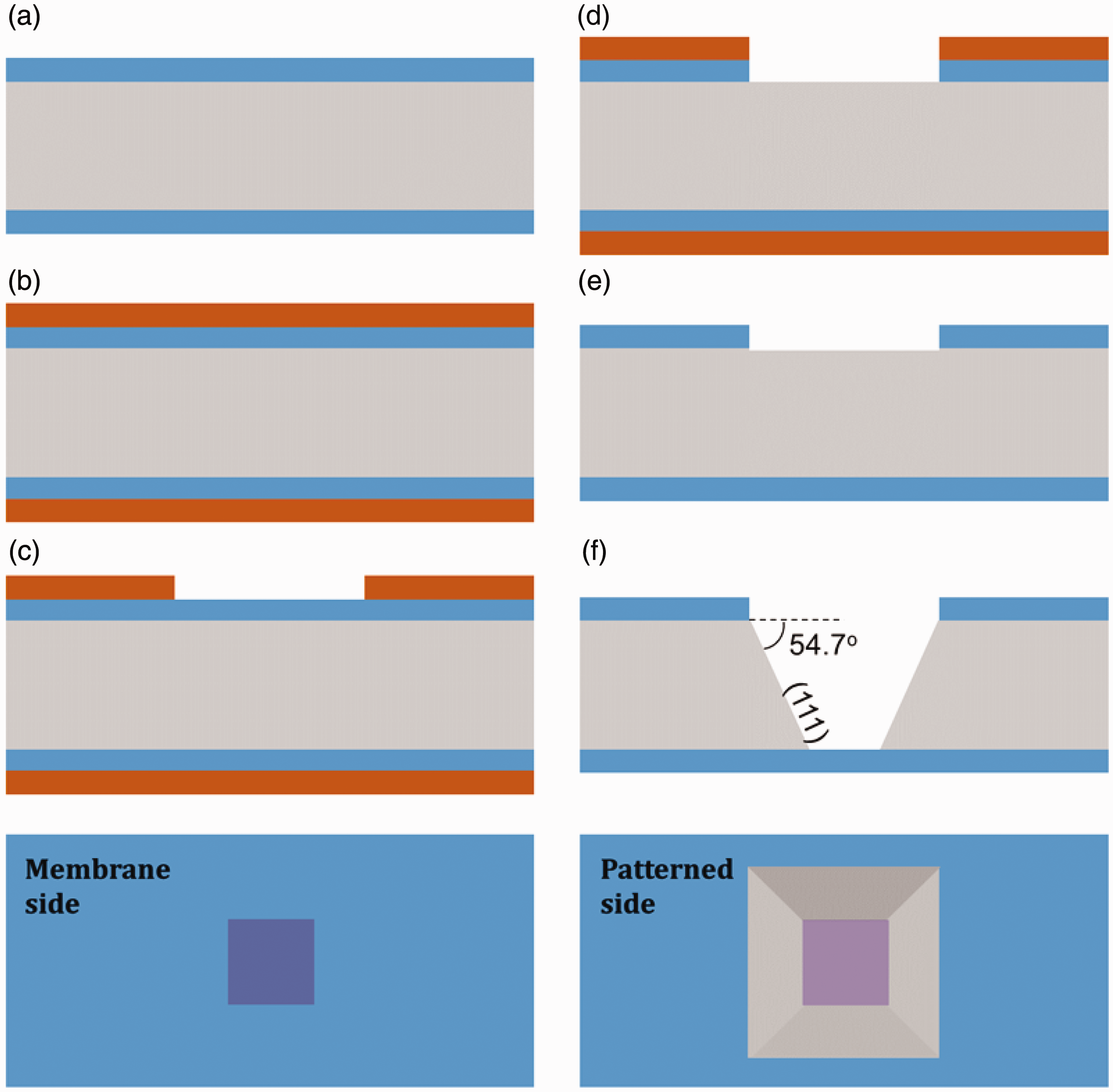
There are various subtleties and practical know-hows to the fabrication process that are beyond the scope of this article. We mention, however, a couple of important ones, both related to the KOH etching process. The fabrication procedure described above assumes that SiNx is a perfect KOH etch stop. Yet, the selectivity of KOH etching for LPCVD SiNx versus Si, though extremely high, is not infinite. While the KOH etch rate of SiNx is not well studied, some sources report selectivity values that range from 1:10 000 to 1:50 000.70,71 The upper limit on the corresponding KOH etch rate of SiNx is 0.1 nm/min. Such an etch rate is not negligible when fabricating ultrathin windows (< 10 nm) and should be taken into account when deciding on the thickness of the LPCVD deposited SiNx layers. The other point relates to the use of doped Si wafers. For certain applications, it is desired to use highly doped Si in order to electrically ground the supporting frame. For instance, this is useful when employing the window as a support structure in electron microscopy, in which the structure is continuously exposed to a high flux beam of electrons. However, using boron-doped Si can significantly retard the KOH etch rate, and, above a certain doping threshold, boron-doped Si can serve as an effective KOH etch stop. 72 Therefore, it is recommend to use n-type doped Si (e.g., phosphorus-doped) for applications where high electrical conductivity is desired, without severely impacting the KOH etch rate.
Mechanical Properties of Free-Standing Silicon Nitride
Low-pressure chemical vapor deposition SiNx deposited on Si possesses an amount of residual stress from two sources: intrinsic stress due to the deposition conditions and thermal stress due to the mismatch in the coefficients of thermal expansion between film and substrate. 73 Even though Si3N4 has a slightly lower coefficient of thermal expansion than Si, resulting in compressive residual stress, the residual stress in LPCVD SiNx tends to be tensile in nature (i.e., the deposited film is elongated relative to a stress-free film). 74 The deposition parameters (temperature, pressure, and gas flow rate) offer a certain degree of control over the amount of residual stress. Moreover, non-standard deposition techniques can be employed to control the residual stress within a wide range of values. For example, Shi et al. demonstrated using ion implantation to tailor the residual stress of SiNx over a range of values extending from 1.2 GPa (tensile) to −0.1 GPa (compressive). 75 In micro-electro-mechanical systems (MEMS)-type devices, however, low residual stress films are highly desirable. While there are reports in literature on fabricating stress-free films, 76 the standard processes that are commonly accessible in nanofabrication facilities produce films with tensile stress as low as ∼200 MPa.
For SiNx windows used as support structures, a mechanical property of interest is the amount of bulging (also referred to as buckling or bowing) due to differential pressure (e.g., pressure applied from one side of the membrane normal to the membrane surface). For example, in nanofluidic devices such as the one shown in Fig. 2b, two SiNx windows and a spacer are used to define a sample path length. 77 In such an application, the effective increase in the path length due to bulging of the membranes could severely compromise the functionality of the device. Thus, it is essential both to characterize bulging and to understand which design features can be used to keep bulging to a minimal acceptable level.
A schematic of the bulging geometry for a square membrane is shown in Fig. 4. Characterization of the bulging profile is typically done with load-deflection measurements.74,78–84 In these measurements, pressure is applied to one side of the membrane and deflection is measured optically under a microscope—calibrated to measure depth through changes in the focal plane. For a square membrane, the load-deflection behavior is found to follow the relationship
(top) Cross-sectional view depicting bulging of a square-shaped silicon nitride membrane of side 2 a and thickness t, due to net differential pressure p. The parameter of interest is the maximum deflection d at the center of the membrane. Maximum deflection of a 100 µm square membrane (center panel) and a 1 mm square membrane (bottom panel) are plotted as a function of differential pressure up to ∼1 atmosphere and for different membrane thicknesses (10, 100, and 1000 nm). The cross marks represent fracture points calculated according to the model in Eq. 2. The fracture model assumes that the membrane has a pre-existing crack line that is 10 µm in length. Absence of a fracture point indicates that the membrane is able to withstand the pressure at least up to the top end of the calculated range.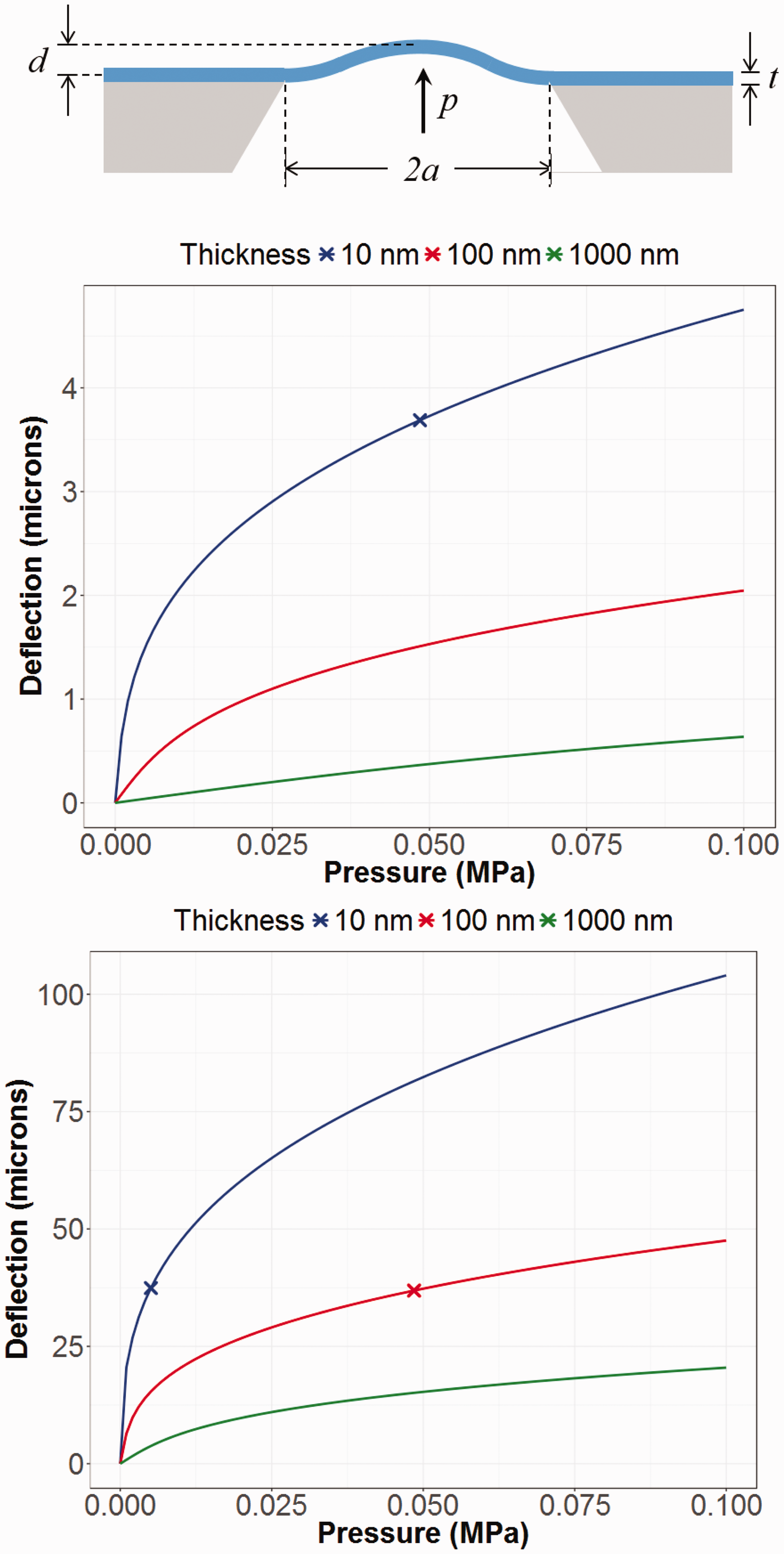

In these calculations of the maximum deflection under differential pressure, it was assumed that the membrane is able to withstand the pressure up to the maximum amount displayed in the plots. In reality, the membrane may fracture at some point as the pressure is increased. The fracture toughness of a membrane is an important materials property that defines the resistance of a membrane to fracture. It is directly related to the lateral stress at which a membrane that contains a crack fails. This property of the membrane is measured using the same load-deflection experiments used to characterize the bulging profile. Previous measurements found the fracture toughness to be in the 6–7 MPa m1/2 range independent of the membrane thickness.81,88 The fracture toughness (

The calculations above give an impression of the sensitivity of the expected amount of deflection and fracture point to window thickness, window dimension, and applied pressure. For devices that use irregular window shapes or where it is desired to map out the exact profile of the membrane deformation, elaborate models of the deformation were developed and tested by Yang et al. 82 Lastly, measurements specific to bulging of nanofluidic cells under liquid flow conditions were carried out in situ using a scanning transmission electron microscope (STEM). 89 Beyond the design and handling considerations imposed by these calculations and measurements, one should be cautious in using ultrasonication as part of a cleaning process, since it can easily rupture the membranes.46,90
Optical Properties of Free-Standing Silicon Nitride
Together with the mechanical stability and ease of fabrication, transparency of SiNx windows is one of the key features that makes them appealing for use as sample support structures in various spectroscopic applications. In applications where light (in the IR, visible, and ultraviolet [UV] range of the spectrum) interacts with SiNx windows, it is important from the viewpoint of experimental design to understand losses due to reflection at interfaces and due to absorption within the window material. In addition to informing design of the experiment, knowledge of the optical properties of the window is key to performing proper data analysis (e.g., in terms of determining the deposited energy within the sample volume in pump–probe experiments). Measurements of the frequency dependent dielectric function of SiNx in the 1–24 eV range were previously performed by Philipp.
91
The dielectric function (left) Experimentally determined complex dielectric function of silicon nitride in the 1–25 eV range (reproduced from measurements by Philipp).
91
(right) The real part of the refractive index as extracted from the dielectric constant. The y-axis scale on the right side shows the reflectance of SiNx at normal incidence.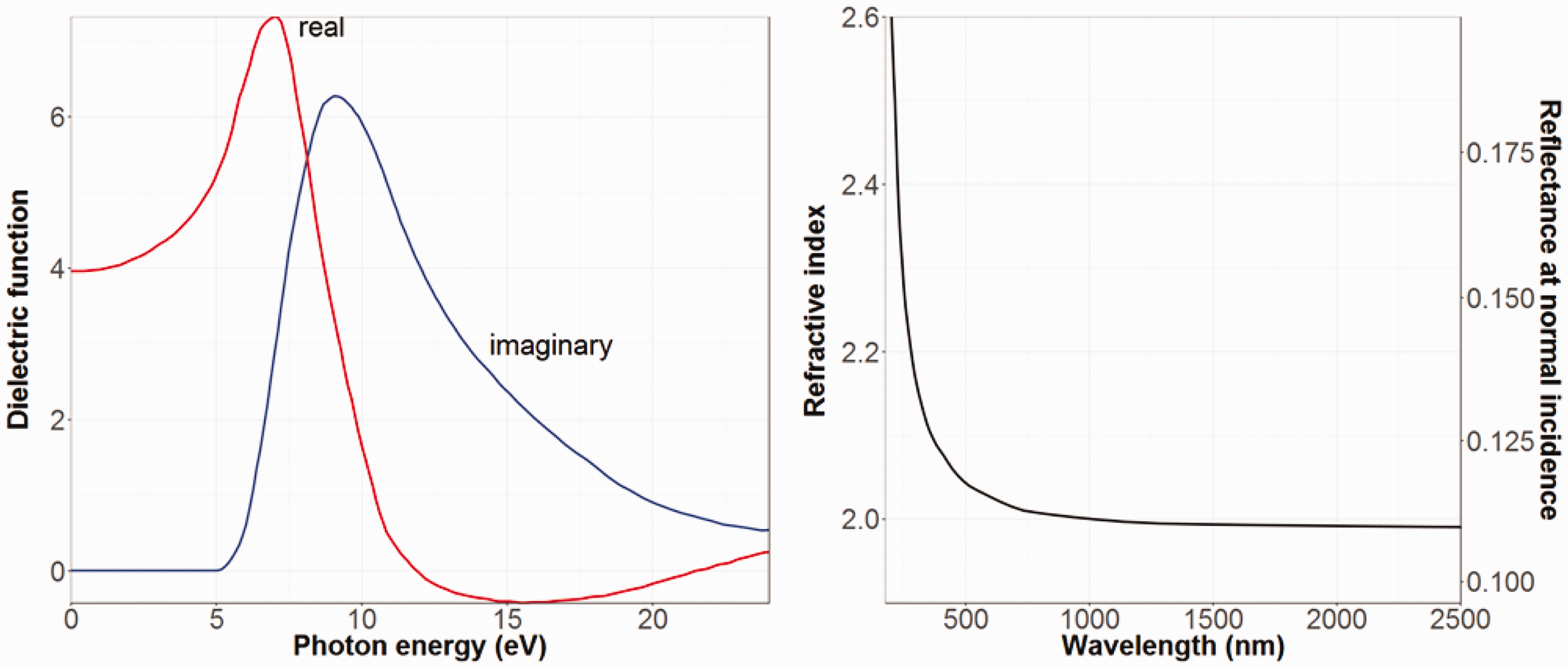

Reflectance of p- and s-polarized light at an air–material interface is calculated from the refractive index according to Fresnel’s equations:
In the above, n is the index of refraction and

Fig. 5 shows that the reflectance at normal incidence can be up to 20% for frequency ranges below the absorption threshold. There are several strategies for reducing the reflectance to near zero. If the experiment does not constrain the angle of incidence and light polarization, reflections can be mitigated by tuning these parameters: the most straightforward approach would be to use p-polarized light at Brewster’s angle (∼63° for SiNx) to totally suppress reflection. Other strategies take advantage of multiple beam interference effects—as in a Fabry–Perot etalon—to suppress reflection for a narrow range of frequencies and angles of incidence. Under this scheme, the thickness of the window itself could be a key parameter to control in suppressing reflections, thereby improving signal quality. The theory of multiple beam interference is well developed and can be found in introductory optics text books.
93
To demonstrate the benefits of tailoring the window thickness according to the application of interest, consider an air–SiNx–water interface. At normal incidence, the reflectivity of the structure varies between

A study by Poenar et al. measured the index of refraction and extinction coefficient of LPCVD SiNx in the 400–800 nm wavelength range using spectroscopic ellipsometry and direct reflectivity measurements.
94
Because of the narrower measurement range compared to the earlier work of Philipp,
91
this study provides better estimates of the extinction coefficient in the visible range of the spectrum. As shown in Fig. 6, the extinction coefficient, Extinction coefficients of several thin-film materials including low stress SiNx (solid lines). Data based on ellipsometry and reflectivity measurements by Poenar et al.
94
BSG and PSG refer to borosilicate glass and phosphosilicate glass, respectively. Reproduced with permission from the Optical Society of America.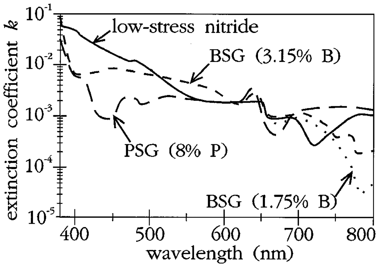
Lastly, a recent theoretical study calculated the dielectric function of silicon nitride using density functional theory. 95 The results were consistent with the measurements of Philipp for β-SiN—a crystalline phase of silicon nitride. The same study also examined both the effect of defects due to excess Si and the effect of hydrogen termination on the optical properties. In both cases, changes in the energy loss spectrum below 10 eV were found, suggesting the possibility of tuning optical properties by controlling the composition and surface chemistry of the SiNx films.
X-ray and Electron Scattering Properties of Free-Standing Silicon Nitride
In applications where SiNx windows are used as X-ray or electron transparent support structures, the main concern is reducing scattering of the probe from the window material. The objective here is twofold: to reduce background signal resulting from scattering off the window; and to avoid severely attenuating the probe beam (be it an X-ray or an electron beam). Obviously, using as thin a membrane as possible would be the ideal strategy. However, there are often other constraints that come into play when designing a suitable support structure. The most important limitation to reducing window thickness is the reduced mechanical stability and, subsequently, the susceptibility of the window to bowing and fracture. Other constraints may include thermal and charge transport properties in applications where large amounts of energy or charge are deposited into the window-sample structure. Fig. 7 shows the X-ray transmission of SiNx windows of various thicknesses as a function of photon energy. In the higher energy range (e.g., above ∼5 keV), transmission is close to unity even when using 1 µm thick windows. In the low energy range (below ∼2 keV), windows with thicknesses above 100 nm have severely reduced transmission. It is therefore recommended for soft X-ray applications to keep the window thickness on the order of a few tens of nanometers.
X-ray transmission of 10 nm (red line), 100 nm (green line), and 1000 nm (blue line) thick SiNx windows. Data obtained from the CXRO database, based on the work of Henke et al.
96
The calculation assumes a density of SiNx of 3.44 g/cm3. The left panel highlights transmission at energies below 2 keV, whereas the right panel is for energies in the 2–10 keV range.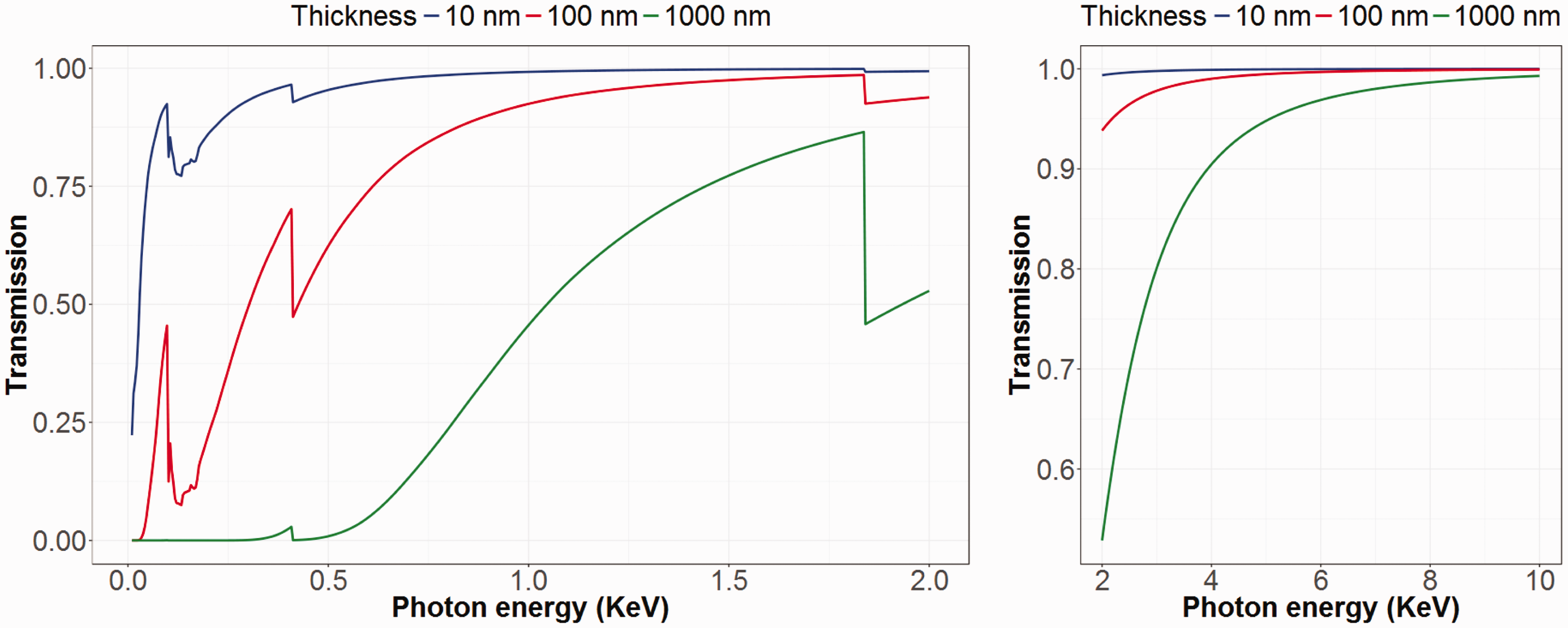
At even lower photon energies, working with thicker windows is not an option and the trade-off between mechanical stability and X-ray transmission becomes more restrictive. To circumvent this problem, certain designs employ a porous membrane structure. For instance, several commercial suppliers of SiNx windows offer what is referred to as “holey membranes.” These membranes are thick enough (∼200 nm) to allow for sufficient mechanical stability, have a large enough window area (∼1 mm2), but contain a number of holes for X-rays or electrons to pass through. The downside of this approach is the limited transmission as defined by the porosity of the membrane (typically below 25%). Alternative approaches implement grid-like support structures to enhance the stability of the film. For example, Törmä et al. fabricated ultrathin SiNx X-ray windows (40 nm thick) with an area as large as 30 mm2. 97 Mechanical stability was achieved by embedding in the window design a grid structure made of polycrystalline Si for additional support. The open free-standing area of the window was 77%.
Electrons interact more strongly with matter than X-rays. Therefore, scattering effects are more severe when employing SiNx windows as support structures in a TEM. There are few data in the literature on the electron transmission of SiNx, but this property can be calculated from the theoretical elastic scattering cross-sections developed by Riley et al. for the 1–256 keV energy range.
98
In order to calculate the electron transmission of the windows, the inelastic contribution to scattering also has to be considered. The inelastic contribution to scattering is derived from the empirical law


In the above, the summation j is over the type of atom. Finally, electron transmission, T, of the SiNx window is calculated from the mean free path by

Fig. 8 shows the electron transmission of SiNx windows of select thicknesses in the 1–256 keV range as calculated from Eq. 8. Note that these calculations are inherently conservative as they assume that any electron that undergoes a scattering event is “lost.” The derivation above can be readily modified to accommodate a more realistic scenario by excluding from the scattering cross-section the angular range within which scattered electrons remain useful to the experimental measurement. This is done by replacing the elastic scattering cross-section, (left) Electron transmission of 5 nm (blue filled circles), 10 nm (red filled circles), 20 nm (green filled circles), and 40 nm (purple filled circles) thick SiNx windows, 5 nm a-C (green open circles), 40 nm a-C (red open circles), and bilayer graphene (purple open circles). Data obtained from theoretical electron scattering cross-sections.
98
The calculation assumes a density of SiNx of 3.44 g/cm3 and a 1:1.1 Si:N stoichiometry. This composition is used to calculate the average scattering cross-section weighted by the number densities of the composite atoms. a-C and bilayer graphene were assumed to have a density of 2.0 g/cm3. The solid lines are trend lines (the original work modeled energies satisfying 2 m keV, with m being an integer between 0 and 8). (right) Selected area electron diffraction (SAED) images of an α-Si3N4 nanorod. The image on the bottom left is for a single crystalline section taken from the body of the rod. The image on the top right is for an amorphous structure corresponding to the tip of the nanorod. Image reproduced from Huang et al.
99
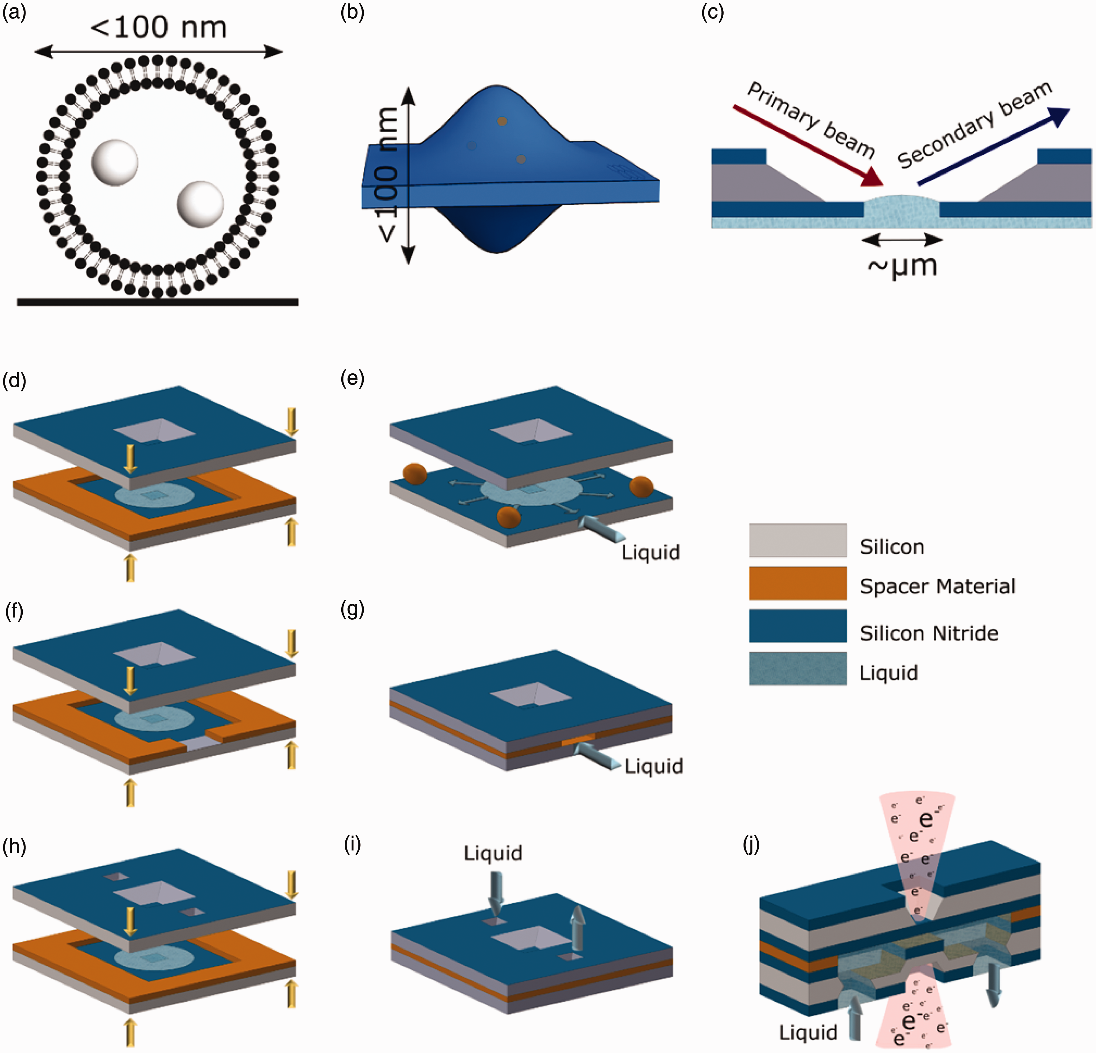
with permission from Elsevier. (a) Vesicles offer nanoscale liquid confinement in soft phospholipid envelopes, with well-established formation protocols. (b) Robust graphene membranes can form nanoscale containers around liquid droplets. (c) Micrometer-diameter openings in otherwise intact vacuum windows provide access to underlying liquid-phase samples (see discussion of SALVI in text). Silicon nitride thin films spanning openings in silicon frames can be used to form a range of nanoscale liquid containers. Cell formats include: (d) those with integral spacers that require sample addition before sealing; (e) those with, e.g., nanoparticle spacers that can be loaded with liquid before or after closing; (f) those with integral spacers allowing (g) liquid loading after closing; and (h) those with an integral spacer but (i) more sophisticated fluidic connections allowing (j) structured flow channels for control over fluid flow useful for, e.g., TEM. Object sizes are not intended to convey scaling information. Figures in (d)–(j) are reproduced from Dwyer et al.
20
with permission of The Royal Society of Chemistry.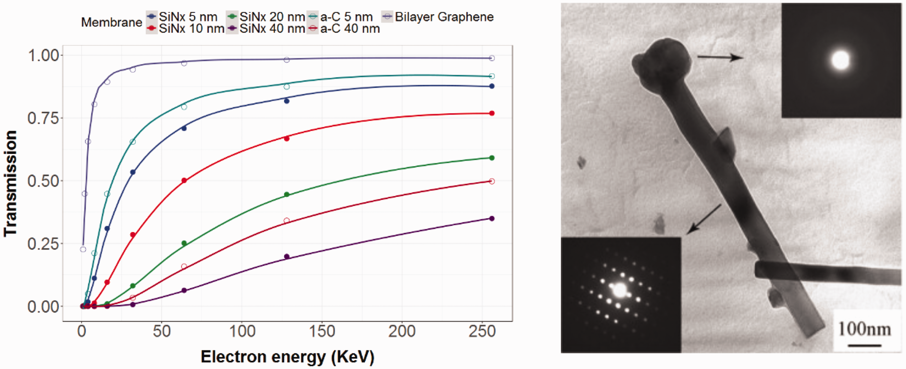
Another important aspect to the use of SiNx windows as support structures for TEM samples is the background signal resulting from the scattering of the electrons off of the window material. Even in the single scattering regime, where the window transmission is sufficiently high, part of the electron beam will undergo forward scattering at angles other than 0° (relative to the unscattered beam direction). Because SiNx is amorphous, the pattern originating from the window has a diffuse character rather than the well-defined diffraction patterns generated by scattering from single crystalline structures. Fig. 8 is an example contrasting the electron diffraction patterns of single crystalline α-Si3N4 and amorphous α-Si3N4. The amorphous pattern is diffuse and contains broad ring-like patterns that correspond to the nearest neighboring distances in the amorphous material. In order to account for the contribution from the window, measurements are typically done on a blank window (i.e., without sample) and the background pattern is subtracted from the diffraction obtained for a sample-on-window structure. Scattering, however, is not strictly additive in this sense, but the approach does not require complex beam propagation calculations. Accounting for background signal is especially important when the sample of interest is not crystalline and will therefore not have the benefit of spatially well-defined diffraction peaks.
When operating the TEM in imaging mode, another concern is the reduced spatial resolution due to inelastic scattering of the electron beam from its interaction with the window material. De Jonge and Ross modeled this effect in nanofluidic cells. 101 The main conclusion was that for ∼1 µm liquid thickness, the window material itself does not contribute significantly to inelastic scattering. Instead, the resolution-limiting factor comes from inelastic scattering of the electrons with the liquid constrained between the cell windows.
Further reduction of electron scattering from the support structure can be achieved with use of lighter membrane material. The most commonly available option for TEM applications are amorphous carbon (a-C) films that are mounted on standard TEM grids. The thicknesses of these films can be < 10 nm. Fig. 8 shows that the transmission of a 5 nm a-C membrane is slightly higher than that of a SiNx membrane of the same thickness. Even higher transmission can be achieved using graphene, few layer graphene (FLG), and graphene oxide support membranes—all of which are commercially available. In Fig. 8, the transmission of bilayer graphene at 100 keV is ∼98%. Yet, even with the higher electron transmission, whether it is advantageous to use SiNx versus a carbon-based support structure depends on the specific application. The SiNx fabrication process is scalable, whereas with graphene and a-C, the support film needs to be prepared separately then transferred onto a suitable TEM grid. Consequently, the transferred film tends to have folds and wrinkles that limit its usable area. More importantly, when it comes to building of devices, SiNx is still more attractive because its deposition and processing are part of the highly standardized nanofabrication processes developed by the semi-conductor and MEMS industries. On the other hand, an important distinguishing feature of graphene and a-C films is their high electrical conductivity—in contrast with SiNx, which is an insulator. It is expected that as progress continues in the fabrication technology of graphene and carbon-based materials, such films will be considered more seriously as viable alternatives for SiNx.
Chemical Properties of Silicon Nitride Surfaces
The surface of silicon-rich SiNx exhibits a rich blend of silicon-, oxygen-, and nitrogen-bearing surface species, whose particular mixture depends strongly on sample preparation and history (including “aging” and, in the case of commercial sources, vendor).20,64,66,102–106 This history dependence can perhaps be appreciated most easily through a survey of the silicon oxynitride (SiOxNy) literature, or through the variability of experimental outcomes when proper care is not taken.66,107,108 A surface oxide coating readily forms in air (and can lead to an oxide gradient into the film),102,108,109 and the susceptibility of Si3N4 to evolve ammonia by hydrolysis in the presence of liquid- and vapor-phase water should also be considered.102,103 In spite of this, SiNx shows very strong chemical resistance to a wide range of etchants and conditions, and indeed, etch resistance is the mechanism by which the film is made free-standing.16,17,65 These films will, however, yield to etching in hot phosphoric acid (which requires quartz or other suitable vessel material).
110
The consequences of this rich tangle of surface chemistry are both fearsome and tantalizing. In aqueous solution, multiple surface acid–base equilibria exist, and one must be attentive to unintended effects arising from the surface charge (and surface charge screening) that can change as a function of solution pH and ionic strength.20,104,109,111–113 Under most conditions, the total surface charge density will reduce to

Here, e is the electron charge, and
Nanofluidic Sample Cells
Experimental efforts to gain ever-greater insight into the molecular world—on ever-faster timescales, with ever-greater spatial resolution, with ever-greater departure from tractable model systems, and with ever-greater diversity of samples—can encounter extraordinary barriers.17,38,39,131–133 In some cases, the challenges arise from the properties of the sample, itself—high optical absorption or scattering cross-sections that require extremely short path lengths, for example.17,38,39 In others, experimental conditions can present challenges as simple, but unyielding, as the necessity for vacuum conditions, or as pernicious as probe-induced sample damage.38,39,134,135 Challenges can be additive and mutually amplifying in severity. The use of a sample container can play a similarly complex role. On the one hand, it may be used to ensure the requisite conditions are satisfied, but on the other hand, it introduces additional matter into the experiment’s path of interrogation. As a concrete example, attempts to use femtosecond multi dimensional IR spectroscopy to study energy redistribution of the hydrogen bonding network in pure water, rather than in isotopically substituted model systems, had to deal with the high optical absorption at the energies of interest that restricted the water layer thickness to ∼500 nm. Attempts to compress the water to the desired thickness between thin diamond windows could easily place at least one of the “sample” challenges in stark relief: expensive cracked windows without successful spectroscopic measurements (personal communication, ca. 2004). An additional challenge of using windows to physically constrain the water path length to submicron dimensions was that even optically transparent windows could generate a non-resonant contribution to the measured signal at short times, thereby potentially obscuring the short-time dynamics of the water. The joint consideration—the need for a well-defined submicron path length in a configuration that did not add on an (appreciable) non-resonant contribution—prompted the design of a sample cell constructed from thin-film SiNx windows around a 500 nm-high fluid channel. 17 The 800 nm-thick windows did not themselves contribute to the signal, which was vital to reveal the ∼50 fs timescale for the decay of the memory of persistent correlations in the hydrogen-bonded network of pure water. The utility of this SiNx material—or its thin-film brethren—for sample cell windows extends across the spectrum and into charged-particle techniques.17–20,35–45,53–58 We note, of course, that there is a tradition of alternative nanoscale sample chambers for spectroscopic studies, including vesicles, micelles, zeolites, and supramolecular entities.136–140 Vesicles, for example, have been used in both ultrafast and single-molecule studies and use well-established formation protocols to use thin, but fragile, lipid bilayers to provide nanoscale confinement and low window signal (Fig. 9a).136,138,139 Pores can be formed through the bilayer to permit limited access to the vesicle interior.136–138 More recently, ∼1 µm thick, window-free liquid samples in vacuum have been achieved and used for transmission soft X-ray studies using a sophisticated arrangement of liquid jets. 141 The performance of this elegant solution is determined by sample properties such as the surface tension, viscosity, temperature, and vapor pressure, where solvent-optimization may lend generality to the study of solution samples using this approach. Nanofabricated equivalents of conventional sample cells and cuvettes,17–20,35–45,53–58 have a number of advantages relating, primarily, to their generality of application. Their construction provides for straightforward manipulation, even by hand, and one has access to materials that can offer a greater range of sample compatibilities—either directly or through modifications—than the materials in specialized implementations such as phospholipid-based vesicles. The basic structure (Fig. 9d–9e) can be modified by a host of conventional and unconventional nanofabrication approaches, allowing the integration of functional and structural elements such as electrodes to allow for more in-depth or flexible investigations.42,142–144 Two additional key advantages emerge. First, the design provides for a convenient macroscopic-to-microscopic interface (Fig. 9f–i). This is seen, on the one hand, by the natural integration of the thin-walled channel with a convenient Si frame. By opening the nanochannel to the edge of the Si frames to create a through-channel, sample could be loaded into the preassembled cell by capillary action or, through appropriate design of a sample chamber holder, through forced flow.17,36,41,42,145–147 Second, the dimensions of structural and functional elements can be readily tuned within the existing fabrication infrastructure in order to adapt to different experimental needs. An exceptionally stringent test for thin-walled nanofluidic cells comes in the context of TEM (Fig. 9j).
Liquid (or “wet”) samples have long held allure for practitioners of (transmission) electron microscopy, but the vacuum environment needed for electron microscopy and the need for < 100 nm-thick samples left the field with only a handful of painstakingly executed early investigations.38,40,143,148–159 Both challenges similarly afflict a broader class of samples than liquids. Sophisticated and elegant solutions have involved reconfiguring the sample-containing region of the electron microscope itself and using low-vapor-pressure ionic liquids to cope with the vacuum conditions.149,156,160–165 Cryomicroscopy rather enviably protects the sample against the vacuum, but suffers from a number of severe limitations: the possibility to observe structural dynamics—such as aggregation, nucleation, electrodeposition, and self-assembly driven processes37,38,40,143,166–169—is essentially eliminated, as is the ability to rapidly exchange samples on-the-fly. 20 A liquid cell for TEM thus holds much appeal. The minimal requirement for such a cell is that it adequately preserve the integrity of a sample, with a thickness suitable for the desired spatial resolution (≤100 nm for higher resolution).36,40,170 This thickness limit includes sample and window thicknesses, weighted by the scattering properties determined by their structure and composition. The channel height (but not window thickness) restrictions are less stringent on gas cells for TEM. 171 Sample cells for SEM on liquid samples face similar challenges in terms of the effective window thickness (as measured by its contribution to signal attenuation), but without the accompanying requirement to also control the sample thickness which will, instead, by determined by the electron beam penetration depth.101,172–175 To fully maximize the potential of in-liquid TEM for exploring nanoscale structure, it is necessary that the nanofluidic cell support through-flow.17,36,41,42,145–147,176 Once such a sample cell is loaded into the electron microscope, with connecting fluid lines external to the microscope, the sample can be easily introduced for examination without the delays of waiting for vacuum to reestablish during conventional sample loading. A sample damaged by the electron beam—either directly or through solvent-mediated damage—can be quickly purged and replaced. Surface chemical treatment (or use of alternative window materials) may be required to suppress unwanted interactions between the sample and window—or to encourage favorable interactions.20,36,177–180 Perhaps the most exciting research frontier is the pursuit of structural dynamics.36,37,41,132,143,167–169,179,181–185 Sample structural evolution can be triggered by changing the liquid composition (e.g., the solution pH, or the solvent polarity, or injecting different constituents such as cross-linkers and denaturants), and then observed with the spatial resolution of the electron microscope.
The promise of this new generation of conventional nanofabricated fluid cells for TEM was first demonstrated in 2003. 37 In brief, the cell was hand-assembled using vacuum-compatible epoxy to seal two 100 nm-thick SiNx windows around a 0.5–1 µm-high ring of SiO2. A particularly exciting element of this particular cell was the inclusion of electrodes, a configuration that allowed for directly triggering the structural dynamics: electrodeposition of copper within the cell. The two key structural advances of this cell were the use of thin SiNx windows and the incorporation of a hard spacer to define the liquid channel height. More streamlined fabrication approaches have tackled the limitations of using hand-applied epoxy to seal the cell: thin-film indium can serve to seal the sample cell and define the liquid reservoir height; direct wafer bonding has also been used for cell sealing and is compatible with the use of well-defined hard spacers to define the liquid channel height.42,167 There is considerable variability and flexibility—depending on acceptable performance specifications—in the construction of devices using thin-film windows in a Si frame (e.g., SiNx, SiO24,6–10,186,187), including using hand-applied epoxy as spacer and for bonding (for a ∼5 µm gap), hand-applied nanoparticles as spacers, and patternable photoresist spacers.20,36–38,40,42,43,179,188
Recent advances in materials science have broadened the choice of window materials beyond traditional nanofabrication materials and, in a sense, have resurrected the use of thin, carbon-based films. The principal advantage of such a material choice is of course that the low (average) atomic number and low atomic density have salutary effects on image contrast and resolution. 101 Of course, the materials—true for all such windows—must offer sufficient mechanical robustness, electron-beam resistance (including conductivity when charging is a concern), and chemical compatibility with the sample. The limitations of using conventional carbon-based polymer thin films as windows for TEM fluid cells were seen quite clearly in early developments in building cells for using SEM to examine wet samples.101,175 Of a number of carbon-based films tested by Moses et al., only polyimide was found to be suitable, and then with a window thickness of 145 nm (50 nm could be achieved if a small leak was introduced into the microscope chamber), and without being used to constrain a thin liquid layer.101,175 Carbon nanomembranes, a recent, ∼1.5 nm-thick, addition to the TEM support film toolkit, may hold promise for designing fluidic cells.5,11,189,190 Large-area carbon nanomembrane films can be readily manufactured, but their more compelling characteristics stem from their synthesis by electron-beam-induced cross-linking of molecular precursors. One can choose from a variety of molecular precursors that will all generate ultrathin carbon-based films that can subsequently be chemically functionalized with relative ease. 190 Thus, the film properties of these ultrathin, carbon-containing films can be determined with molecular-level control. 190 In contrast, graphene offers a set of prospects determined by its unique composition and structure. Graphene, though, has received considerable attention in the field of TEM of liquid samples.38,179,183,191,192 Liquid-containing “nanobubbles” (Fig. 9b) can be formed between two graphene sheets laid together, reminiscent of earlier work using ∼30 nm-thick “hard” carbon films. 150 The formation and size of these nanochambers is not directed and so sample-containing regions suitable for study must be found. In a sense, the use of this cutting-edge material has brought the “sample question” of TEM—and of TEM on liquids—full-circle: the nanocontainers are closed (aside from leaks; the contents are not added or exchanged after container formation) and the assembly is essentially by hand. As the fabrication footprint for graphene matures, however, assembly should become more deterministic and more sophisticated graphene-windowed fluid cells for TEM will undoubtedly emerge. Nevertheless, these graphene-bounded liquid cells have set the standard for imaging resolution, through the use of windows a single atom thick, where that atom is of low atomic number, and with achievable liquid path lengths of tens of nanometers.38,179,183,191 Nanofluidic through-flow grants incredible capabilities and for both breadth of study and depth of discovery, must remain a focus of effort, regardless of the particular window material or assembly process.17,36,41,42,145–147,176
Many of the most impressive advances in thin-walled nanofluidics are driven by the demands of TEM, but have tremendous cross-over potential for other investigations. The stringent requirements of the sample cells for TEM may lead to designs that have base capabilities greater than those required by a different technique—SEM, for example, needs not have the thin sample path lengths of TEM—but the additional capabilities may nevertheless be beneficial. For example, when a particular sample cell limits the sample to, for example, a 100 nm-thickness, and a particular technique’s penetration depth exceeds that depth, the sample (cell) itself will provide ∼100 nm vertical resolution without the need for additional mechanisms. Thin-film SiNx windows find use also in XPS studies under ambient, or reactive, environments.193–196 If one is willing to accept (and in fact, design for) the otherwise ostensibly nightmarish prospect—aside from the nanopore sensing paradigm discussed below—of a hole in a liquid cell window chosen for its impermeability, then one may gain even greater experimental access to the chemical processes occurring in liquids (Fig. 9c). 197 A custom-designed vacuum compatible microfluidic electrochemical device was created with a thin-film SiNx cover. By forming a ∼2 µm hole in that cover, the authors were able to then use in situ liquid secondary ion mass spectrometry (SIMS) to probe the electrochemistry, including the electrode-solution interface. 198 A similar fluid cell—one with protected thin-film SiNx window with a single micrometer-scale breach to allow unfettered access—had earlier allowed the characterization of a single cell by both super-resolution optical microscopy and time-of-flight secondary ion mass spectrometry (ToF-SIMS) and the combination of SEM and ToF-SIMS.173,199 The compatibility of this platform of a micrometer aperture in a thin SiNx membrane with a range of characterization tools has led to the coining of the term System for Analysis at the Liquid Vacuum Interface (SALVI).198,199 The performance of this platform has been well-established and was recently anchored in a mini-review of in situ monitoring of catalytic processes in aqueous environments. 200 The available fabrication tools for Si-based cells, coupled with favorable material properties, allow for other functional architectures such as integrated microwells instead of a single sample volume. 201
Beyond structural modifications of the basic nanofluidic platform, advanced detection schemes can be used to compensate for some material and fabrication limitations, and implementation of different experimental techniques can broaden the achievable insights (Fig. 1a). For example, an annular dark field detector can be used to yield atomic number contrast. Thus, when samples themselves offer low contrast—a prime example being biological material in a surrounding aqueous medium 101 —spatial resolution can be enhanced by using an annular dark field detector in conjunction with heavy-atom-containing labels such as gold nanoparticles.34,202–204 This approach was used to enhance the spatial resolution in a fluidic cell for TEM where the liquid path length was micrometers thick, instead of the desired nanometer thickness.34,202–204 Electron energy is also an important consideration when developing optimized sensing schemes—whether it be the incident electron energy or the transmitted electron energy. For example, energy-filtering of the electrons just before detection can improve the spatial resolution of the image, albeit it at the cost of detected electron intensity.11,40,205,206 Energy discrimination of the sample-transmitted electrons leads naturally to a dramatically broadened scope of sensing capabilities, including electron energy loss spectroscopy (EELS),89,207,208 and to perhaps its ultimate extension, vibrational spectroscopy by EELS, with extremely high spatial resolution and different selection rules than optical approaches. 209 By opening up the interior of the TEM to liquid-compatible samples, other investigation tools become available, including X-ray energy-dispersive spectroscopy (XEDS) 210 and time-resolved studies including and extending well beyond dynamic TEM (DTEM).131,132,169
Nanopore Single-Molecule Sensing
Typical nanopore devices are constructed from the basic structure outlined in Fig. 2c, a nanofluidic channel through a thin, free-standing SiNx membrane. Nanopore holders are constructed so that this nanopore provides the sole fluid path connecting electrolyte solutions on both sides of the membrane. The insulating, impermeable SiNx thus acts as a physical barrier and as a support for the channel through which ions and molecules can pass under the influence of an electric field or other suitable driving force.21–29,211–216 The most common sensing configuration is the so-called resistive-pulse sensing mode (Fig. 10). In brief, ions pass through the nanopore in response to the applied cross-membrane electric field, giving a typically pico- to nanoampere current. The nanopore conductance magnitude is determined by the solution conductivity (and solution pH, through its effect on surface charges), nanopore size and shape, and also by the nanopore’s surface charge.24,113,217–221 Passage of an analyte through the nanopore can generate a perturbation in the measured current that arises from physical displacement of solution ions by the analyte and from more complex interactions between charges in solution and on the surface of the analyte and nanopore.24,28,52,221–223 It is convenient to generically refer to the current perturbations as “blockages,” although analyte properties and sensing conditions may lead even to current enhancements.
221
With suitable nanopore and experimental design, the measured current perturbation generates a signal from a single molecule at a time that can be used for chemical identification or profiling. Nanopores can also be used in alternative sensing schemes, including for force spectroscopy and single molecule optical sensing, that will be outlined after a brief discussion of their fabrication.
(a) Schematic of a typical nanopore experimental setup showing the nanopore-containing membrane separating two reservoirs, with electrolyte filling the wells and the pore. The measured current is generated by a voltage applied across the nanopore that drives electrolyte ions (light blue) through the nanopore. Passage of a molecule or particle of interest (orange) through the nanopore can perturb that current. (b) Molecular recognition can augment the sensing selectivity. The complex between analyte and aptamer—the molecular recognition agent—prevents the aptamer from travelling through the pore before it dissociates from the target—a process indicated here by the increased current perturbation duration in the presence of target. Fig. (a) reproduced from Dwyer et al.
20
with permission of The Royal Society of Chemistry.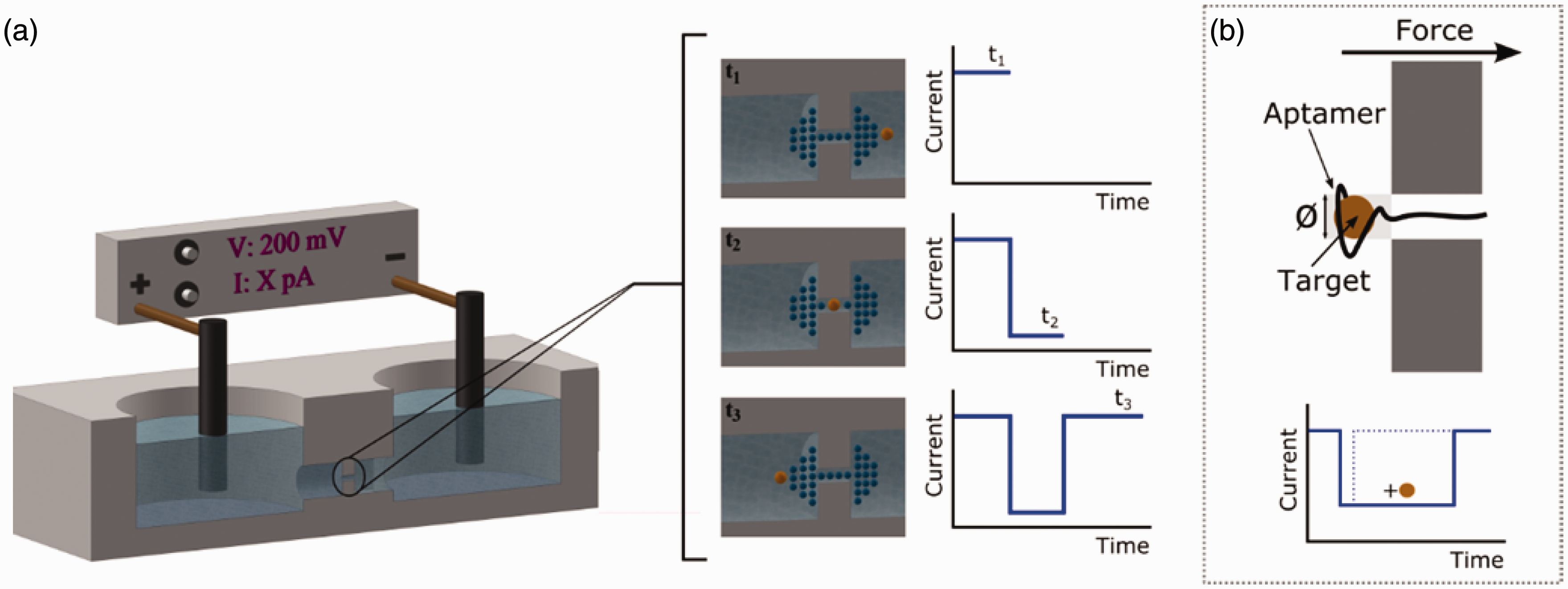
Thin-film SiNx is a standard material for nanofabrication, but small-diameter (< 10 nm), solid-state nanopores formed in thin-film membranes historically represented extreme fabrication challenges. Laborious efforts requiring significant operator expertise saw charged-particle milling—in transmission and scanning electron microscopes, by focused ion beams, or in helium ion microscopes, for example—deliver the desired structures, albeit with fabrication yields that dramatically diminished with sizes < 50 nm.21,23,25,27,144,224–231 Chemical etching of damage tracks left in thin Si-based thin films by relativistic ion bombardment can produce single nanopores and (irregularly spaced) nanopore arrays, but the approach does require the use of large-scale facilities. 232 More specialized approaches exist alongside efforts to draw on conventional techniques such as atomic-layer deposition (ALD).21,23,25,27,144,224–227,230,233,234 Dielectric breakdown has emerged as a simple, yet extremely flexible and powerful, technique to fabricate nanopores: it requires little more than the usual apparatus used for nanopore sensing and instantly wets the nanopore (contrary to TEM-based methods, for example, where surface contamination poses wetting and other challenges).235–237 In overview, nanopores as small as 1 nm in diameter and ∼10 nm long can be fabricated with some flexibility in fabrication method. Characterization of nanopores can be done using charged-particle microscopes and related techniques such as electron tomography and EELS,219,220,238–241 or by much less instrumentally intensive (ionic) conductance-based approaches.113,217–220 A conductance-based characterization is gentler than charged-particle-based approaches and is also more naturally connected to the nanopore surface chemistry—especially to any organic monolayers that may be damaged in the TEM, for example—and to the usual measurable of nanopore single molecule measurements (that is, to the ionic current as a function of time). The advantages of using a conventional nanofabrication material are seen naturally in applications, some of which are outlined below, in which additional functional elements are added to the base nanopore nanofluidic platform. Nevertheless, efforts to continue to develop nanopores using other thin-film materials such as molybdenum disulfide, but with graphene seemingly foremost among them, continue; approaches often see the use of an underlying thin-film SiNx support.242–248 While lacking the electronic properties of graphene, carbon nanomembranes (see discussion above) present an appealing potential ultrathin carbon-based alternative. 249 Nanopores, fabricated using a suitable selection of means and materials of construction, and employed in a variety of configurations and approaches, are an exciting and promising motif for single molecule sensing, confinement, and manipulation.20,21,23,27,28,59,222,250–270
Non-Optical Single-Molecule Sensing
The conventional approach to nanopore sensing, so-called resistive-pulse sensing, 222 treats the nanopore as a nanofluidic channel through which dissolved ions and analytes pass, and with the presence of the transiting analyte registered as an electronically registered current perturbation. Analyte properties are revealed, or at least suggested, by the current perturbation properties such as depth, duration, and fluctuation statistics. In other words, a large number of signal determinants—driving force (usually electrophoretic), solution properties (especially pH and ionic strength), nanopore size and surface chemistry, and, critically, analyte characteristics including size and charge distribution—are collapsed onto a single signal channel. The operational simplicity of this basic sensing paradigm places limits on the analytical selectivity that can be overcome without using additional measures compatible with nanopore sensing (below), but the single molecule sensitivity—without the need for sample labeling or amplification—comes with an ease of operation that exceeds that of most other single molecule methods. Moreover, there are vitally important application areas where sample complexity is not an issue. In the case of DNA sequencing, for example, the challenge is to distinguish between only four unmodified DNA bases and to detect a small number of epigenetic modifications, but to do so rapidly and ideally without significant sample processing that might introduce artefacts.59,271,272 Alternatively, nanopores can be an exquisitely useful quality assurance tool even in complex, many-component samples: the departure of measured current perturbation statistics from those measured on a certified standard sample will indicate the presence of an impurity. In applications requiring greater selectivity, molecular recognition agents such as aptamers can be used as an adjunct to conventional nanopore sensing. In one possible configuration, the interior of the nanopore is functionalized with the molecular recognition agent, making the nanopore responsive to the given analyte (one can envision some implementations functioning as a < 100 nm-long affinity column for a single molecule at a time).211,273 In another, aptamers are released into the sample and the current perturbation characteristics accompanying the partitioning of the aptamer-analyte complex into, or through, the nanopore provides the selectivity.274–277 Binding of an aptamer to its target can drive and stabilize an aptamer conformation change (or stabilize an existing conformation). If, as illustrated in Fig. 10b, the complex is too large to enter into the nanopore, the current perturbation could last until, for example, the complex was ruptured allowing unfolded aptamer passage again.275,276,278–281 The use of the nanopore as a fixed aperture (or as a region of high electric field) to rupture intermolecular complexes, or to disrupt intramolecular interactions, are particular applications of the general approach of nanopore force spectroscopy (NFS), which can be used for bioanalytical applications such as genotyping, and for more fundamental investigations such as exploring receptor–ligand interactions, protein folding, and biologically important interactions between macromolecules.252,253,260,261,282–287 The details of the interactions are mapped onto the ionic current signature. While NFS offers a compelling alternative to other force microscopes 288 for a number of investigations, there are also a number of interesting uses of nanopores in conjunction with AFM and laser optical tweezers.258,284,289–294
Nanopore sensing selectivity can also be improved without molecular recognition agent adjuncts by incorporating different sensing mechanisms that may rely on adding sensing elements to the conventional platform (Fig. 1b). Here, the mechanical robustness and nanofabrication compatibility of the traditional SiNx platform allows for structural and functional elements to be integrated into the nanopore platform, in as straightforward a manner as is allowed by the extreme length scales of nanopores. The installation of electrodes proximal to the nanopore opening and orthogonal to the translocation path, for example, holds prospects for electron tunneling (or, e.g., capacitive) measurements on passing molecules.23,59,295–303 Of course, the installation of nanoelectrodes in nanopores for conventional electrochemical investigations has its own exciting prospects.244,295,304 Such extensions beyond resistive pulse-sensing highlight the importance and breadth of application of nanopores for single molecule science, with an implementation free of the instrumentation, and free from sample processing steps, that may be needed for single molecule optical studies. The nanopore platform, though, is powerfully suited to also enhance single molecule optical studies.
Nanopore as Nanofluidic Cuvette and Optofluidic Device
Nanopores possess a number of structural and functional aspects that can be used to enrich single molecule optical studies. At the same time, optical methods can allow for greater insight into nanopore-enabled single molecule studies and the complementary operating paradigms allow for multimodal measurements. During optical interrogation of a nanopore-constrained single molecule, simultaneous electrical measurements (e.g., resistive-pulse sensing or tunneling measurements) can also be performed, or the applied electric field (or chemical gradients, for example), can be used to perturb the system under investigation (Fig. 1b). Key examples of such non-optical sensing and manipulation approaches were outlined earlier. In a largely passive sense, solid-state nanopores offer lateral molecular localization and confinement on ∼10 nm length scales. Much as vesicle-based nanocontainers have allowed molecular passage through lipid-bilayer-incorporated protein nanopores,136,138 the solid-state channel here itself provides confinement but also molecular passage. Indeed, the nanopore can be thought of as a sort of sample chamber of zeptoliter volume where nanopore surface functionalization (Fig. 1b) and solution conditions can define a unique chemical environment and where an entrained molecule can be subjected to a number of perturbations and interrogation methods. Vertical confinement—provided physically by the nanopore membrane and optically by reflective coatings on the SiNx film—yields a number of benefits, with a common effect being detection of a moiety only once it has passed through the nanopore. Fluorescence is the most likely optical technique to be used in conjunction with a nanopore, but one could imagine that a suitably structured gold film, separated by a well-defined nanopore gap containing an analyte, might also be used for surface-enhanced Raman spectroscopy.20,27,46,61,90,267–269,305–315
Extensions to Nanopore Arrays
We conclude our discussion of the merging of physical- and optical-based nanopore sensing and manipulation approaches, with the consideration of nanopore arrays. While much fundamental nanopore work uses single nanopore devices, application throughput can be significantly increased by crafting and adopting devices housing arrays of nanopores.21–29,38,40 We conclude not with a discussion of the general benefits of multimodal nanopore array-based measurement, which can be understood as array-based extensions of earlier discussions, but rather by focusing more specifically on two final porous thin-film platforms. Track-etched polymer membranes, with < 100 nm diameter pores with number densities as high as ∼109 cm−2, find widespread use as filters.316–319 The ∼100 µm membrane thicknesses, coupled with often tortuous paths, can degrade filtering speed. In contrast, suitable thin membrane filters—such as those fabricated from thin-film SiNx—allow for much higher flow rates.13,47–50,52,69,232,249,307,320,321 When formed using nanofabrication-compatible materials, these porous thin-film platforms can be readily integrated into devices and moreover modified to generate functions beyond filtering. Nanopore filters coated with suitable coinage metal films can combine filtering with surface-enhanced Raman spectroscopy (SERS).46,305,322,323 One particularly interesting application area depends on the ability to control the size and position of the nanopores, so that after metallizing them, they form a plasmonic array.60,61
Conclusion
Free-standing thin-film structures feature both prominently and unobtrusively in a wide range of tools and methods for molecular-level research. Suitable thin films can provide transparency through composition and path length, and that transparency can extend across a wide range of spectroscopically and crystallographically important wavelengths to include charged-particle transparency. Highly localized micro- and nanoscale apertures can be opened in sufficiently robust films when transparency cannot be otherwise achieved. Such transparent, or locally transparent, thin-film window constructs thus enable studies ranging from linear and ultrafast spectroscopies across the visible, IR, and X-ray to X-ray photoelectron spectroscopy, mass spectrometry, and transmission electron microscopy, and many others. A less inconspicuous role uses the mechanical properties of particular thin-film windows to not merely contain samples within well-defined environments, but to provide protection from severe challenges to sample integrity such as vacuum conditions necessary for some experimental methods. The use of thin-walled nanofluidic cells to allow transmission electron microscopy on liquid samples is but the most dramatic of such a role. Thin-film elements can be more forcefully engaged, as seen in nanopore single molecule sensing applications. Nanochannels formed through thin films and having tailored size, shape, and surface chemistry, can be used as a powerful class of tool for single molecule sensing and manipulation. The capabilities of this basic element, alone, have dramatically expanded the toolkit of single molecule science, but it can be even further expanded when additional functional elements and techniques can be integrated with the core nanopore structure. Thin-film SiNx membranes, by virtue of their composition, properties, structure, and fabrication compatibility and infrastructure, figure prominently in all of the structures, devices, and approaches featured in this review article. We therefore used this canonical structural and functional element to demonstrate key performance criteria and principles that will govern the development and application of new materials and structures. Free-standing thin films are truly an enabling element for molecular science.
Footnotes
Acknowledgments
The authors thank Y.M. Nuwan and D.Y. Bandara for their assistance with some figures.
Conflict of Interest
The authors report there are no conflicts of interest.
Funding
JRD acknowledges the support of funding from NSF CAREER award CBET-1150085 for nanopore sensing research.