
Abstract
The jitter measurement floor of a broadband sampling oscilloscope represents an effective lower bound for time-domain jitter measurements and can limit the accuracy of low-jitter characterization. Because characterization procedures can be complex and the results are affected by multiple coupled test conditions, this paper develops a systematic time-domain framework for characterizing the jitter measurement floor. A reproducible measurement setup based on a low-jitter signal source is established, and the effects of vertical sensitivity, input frequency, and input amplitude on the jitter measurement floor are quantitatively evaluated. Based on these results, a rapid parameter-sweep and screening procedure is presented to quickly determine the parameter setting range associated with a near-minimum jitter measurement floor. To reduce reliance on ultra-low-jitter reference sources, simulations and experiments are conducted to examine the relationship among the measured jitter, the source jitter, and the jitter measurement floor of the oscilloscope; the results are consistent with a root-mean-square combination model. Leveraging this model, a root-mean-square-based method is introduced to extract the jitter measurement floor, which remains applicable when an ultra-low-jitter source is unavailable. Experimental results support the effectiveness and practical feasibility of the proposed workflow, suggesting an accessible route toward reproducible time-domain characterization of the jitter measurement floor of sampling oscilloscopes.
Introduction
The jitter measurement floor is a key performance metric of broadband sampling oscilloscopes. It arises from the combined contributions of sampling-clock jitter and noise, which manifest as random jitter within the instrument and thereby degrade measurement accuracy. 1 Some manufacturers primarily characterize the jitter measurement floor in terms of sampling-clock jitter; however, noise can also elevate the floor substantially, and describing the floor solely by sampling-clock jitter is therefore incomplete. Because the jitter measurement floor is superimposed on the signal under test, it biases the estimation of the true signal jitter. In general, a lower jitter measurement floor corresponds to higher measurement resolution and more reliable characterization of low-jitter signals.
The bandwidth of the new generation of broadband sampling oscilloscopes can reach hundreds of gigahertz (GHz), yet their jitter measurement floors can be reduced to as low as a few hundred femtoseconds (fs), and can be further lowered to below 50 fs when a precision time-base module is used.2,3 Meanwhile, advances in crystal oscillators and phase-locked loops have continued to reduce the jitter of signal sources to the picosecond and even femtosecond regime. As a result, the influence of the oscilloscope's jitter measurement floor becomes increasingly significant in low-jitter measurements. It should be noted that the jitter reported by an oscilloscope typically reflects the combined effects of the input signal jitter and the jitter measurement floor; when the input signal jitter is sufficiently smaller than the jitter measurement floor, the measured jitter can be used as an approximation of the floor. Based on this premise, some manufacturer-recommended procedures inject a low-jitter source into the oscilloscope and adjust measurement settings and input frequency to obtain a smaller jitter measurement floor. However, such “source–instrument” approaches often assume that the input signal is “sufficiently low-jitter” without independently quantifying the source jitter or evaluating its uncertainty and impact on the measured result. This limitation may reduce the verifiability and reproducibility of the reported floor, particularly in a scientific research context. Beyond manufacturer documentation, the open literature remains relatively limited in providing systematic measurement workflows, condition-dependent characterization, and practicable evaluation methods when ultra-low-jitter sources are unavailable.4,5
To address these issues, this paper proposes a systematic time-domain framework for characterizing the jitter measurement floor. The main contributions are twofold: a reproducible measurement setup based on a low-jitter source is established to quantitatively evaluate the effects of vertical sensitivity, input signal frequency, and input signal amplitude on the jitter measurement floor, and a rapid parameter-sweep and screening procedure is developed to identify parameter ranges associated with a near-minimum jitter measurement floor; simulations and experiments are conducted to validate the root-mean-square model among the jitter measurement floor (JMF), the input signal jitter (JS), the oscilloscope's measurement of the jitter of the signal being tested (Jrms), based on which a root-mean-square-based extraction method is introduced to estimate JMF when the conventional “low-jitter approximation” is not well satisfied or when an ultra-low-jitter source is not available. Experimental validation indicates that the proposed workflow is effective and practically implementable, providing an accessible route to reproducible time-domain characterization of the jitter measurement floor in broadband sampling oscilloscopes.
Analysis of factors affecting the oscilloscope jitter measurement floor
The concept of an oscilloscope jitter measurement floor
Broadband sampling oscilloscopes use the principle of equivalent sampling to reconstruct and display signals by down-converting them, effectively addressing the challenge of data acquisition for ultra-high-speed broadband signals. 6 Figure 1 provides an illustration of the sampling principle using a pseudorandom binary sequence (PRBS) as an example. The triggering signal triggers the oscilloscope at the same position in each cycle of the periodic signal. To ensure equivalent sampling of the periodic signal after each trigger, a delay of the same magnitude as the previous sampling is added for each sampling instance. This requires the use of a sampling clock. However, due to the imperfections of hardware devices, the oscilloscope itself has a certain amount of noise, and the sampling clock also exhibits some jitter. Therefore, the signal reconstructed by the oscilloscope contains more jitter than the original signal. In other words, the jitter measurement value of the oscilloscope does not directly correspond to the actual jitter of the signal and instead includes a certain amount of error introduced by the oscilloscope's own jitter during the measurement process. This portion of the jitter is referred to as the oscilloscope's jitter measurement floor.
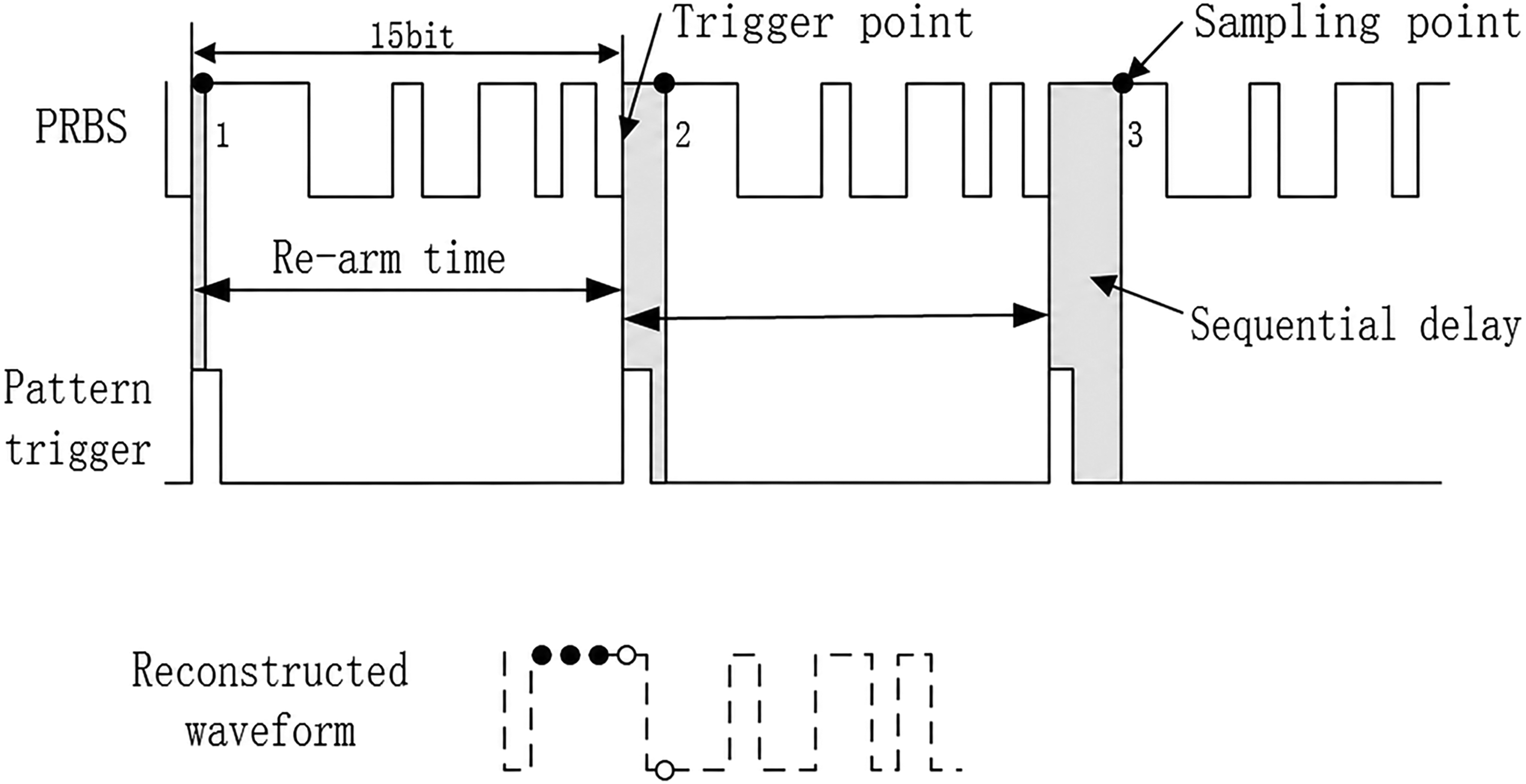
Sampling principle schematic diagram of sampling oscilloscope.
Factors influencing the oscilloscope jitter measurement floor
Detailed explanations are provided through simulation experiments 4 on the factors influencing the oscilloscope jitter measurement floor, including the internal sampling clock jitter, the noise in the oscilloscope's analog front-end and digital processing, and the input signal frequency. The sampling clock is an essential component of the oscilloscope's analog-to-digital converter, and its performance directly determines the oscilloscope's overall performance. 7
The noise in the oscilloscope's analog front end is primarily caused by the attenuator and preamplifier. The function of the attenuator and amplifier is to scale the measured signal for appropriate display on the oscilloscope screen. However, when the signal is attenuated or amplified, the noise is also attenuated or amplified in proportion. Therefore, both the vertical sensitivity and the input signal amplitude of the oscilloscope affect the noise in the oscilloscope's analog front end. 4
The jitter measurement floor depends not only on noise but also on the input signal frequency. As shown in Figure 2, for two signals with the same amplitude, the signal on the left has a higher frequency than the signal on the right. The jitter value produced by the noise superimposed on the signal on the left is smaller than that on the right.
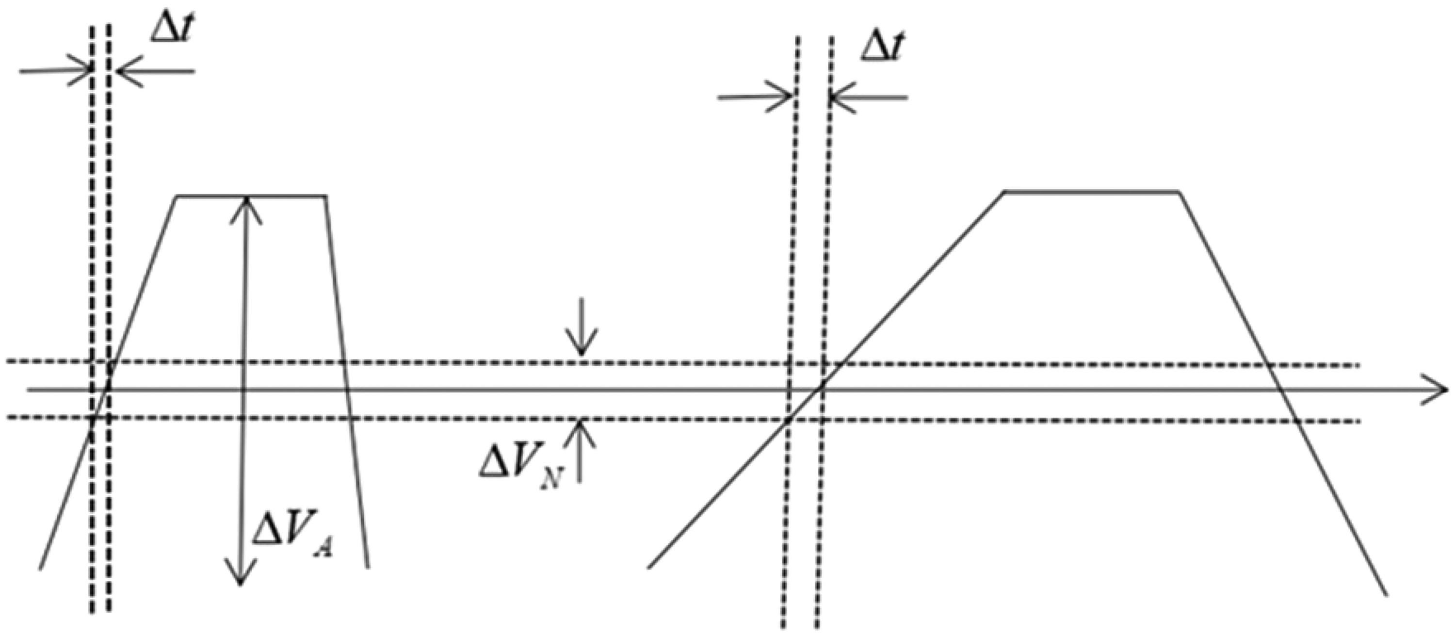
Illustration of the impact of noise on jitter measurement floor.
Building a measurement system for the oscilloscope jitter measurement floor based on a low-jitter signal source
Measurement of signal source jitter
Because the jitter of a low-jitter signal source can be below the oscilloscope jitter measurement floor, direct oscilloscope-based measurement is often impractical. This raises the need for an alternative means of quantifying the source jitter. Therefore, we adopt a time–frequency-domain approach that converts phase-noise information into an equivalent time-domain jitter.
Phase noise is the random fluctuation of phase in a continuous periodic signal and is a crucial parameter for characterizing signal spectral purity and short-term frequency stability. Phase noise is a parameter in the frequency domain, and there is a corresponding parameter in the time domain, jitter.
8
There is a certain mathematical relationship between the two, and they can be converted into each other9,10,11,12,13,14 by equation (1). Therefore, a phase noise analyzer can be used to measure the phase noise of a low-jitter signal source and convert it into jitter in the time domain.

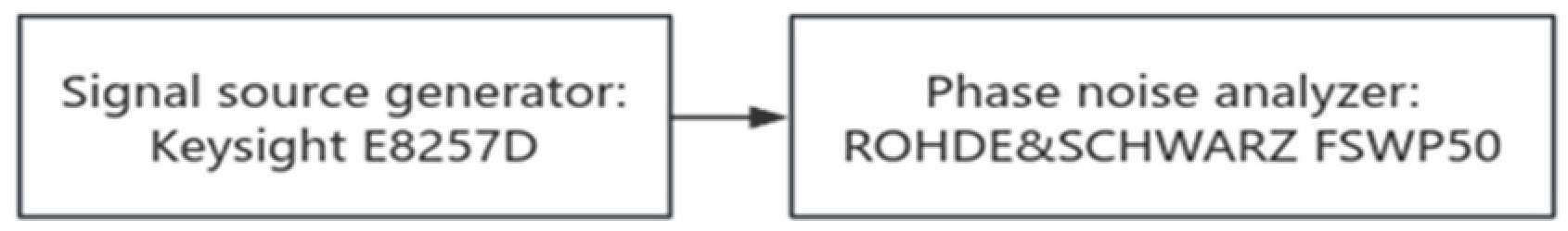
The phase noise analyzer can internally calculate jitter based on the set frequency offset range. A high-performance vector signal generator Keysight E8257D can provide input signals at different frequencies and generate signals with low jitter. 15 When measuring the jitter of a low-jitter signal source using an oscilloscope, there may be significant errors between the oscilloscope's measurement of the jitter of the signal source and the actual jitter of the signal source. Therefore, in this study, a Rohde and Schwarz FSWP50 phase noise analyzer is used to measure the jitter of the input signal source.
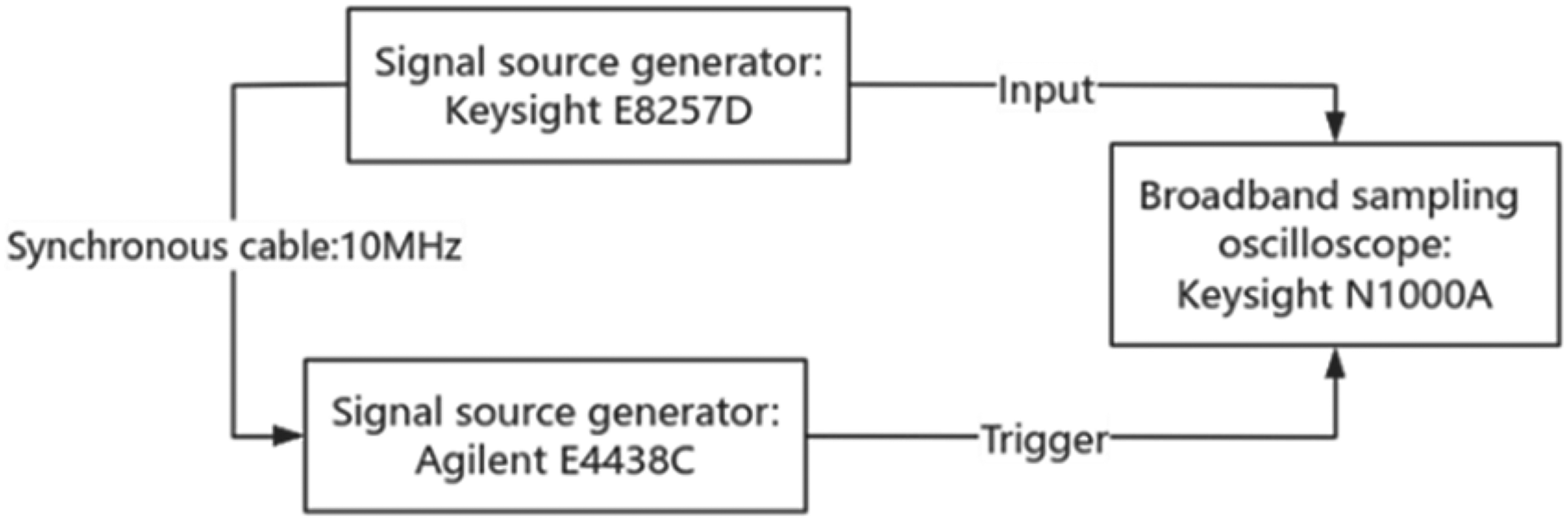
According to the manufacturer's specifications, the FSWP50 phase noise analyzer features very low residual phase noise and high measurement sensitivity. 16 Under the test conditions used in this study, its contribution to the measured jitter is expected to be limited compared with that of the signal source and is therefore treated as a secondary error source. On this basis, the jitter value measured by the phase noise analyzer is used as the signal source jitter JS in this work. The system connection diagram for measuring the signal-source jitter with the phase noise analyzer is shown in Figure 3.
Setup for measuring source jitter using the phase-noise analyzer.
As shown in Figure 4, the phase-noise energy of the tested signal source is concentrated mainly in the small-offset region near the carrier. In this work, the offset-frequency range is set from 1 Hz to 100 MHz (Start Offset = 1 Hz, Stop Offset = 100 MHz). The results show that the phase-noise spectral density is dominated by the low-offset range of 1 Hz to 10 MHz, while it changes only slightly and remains nearly flat over 10 MHz to 100 MHz. This suggests that, under the test conditions used in this study, the low-offset region contributes most of the integrated phase noise, whereas the incremental contribution from the higher-offset region is relatively small. Therefore, 100 MHz is selected as the upper integration limit because it can approximately cover the effective offset-frequency range relevant to jitter estimation in this work, and the integrated jitter is used as an approximation of the signal jitter.
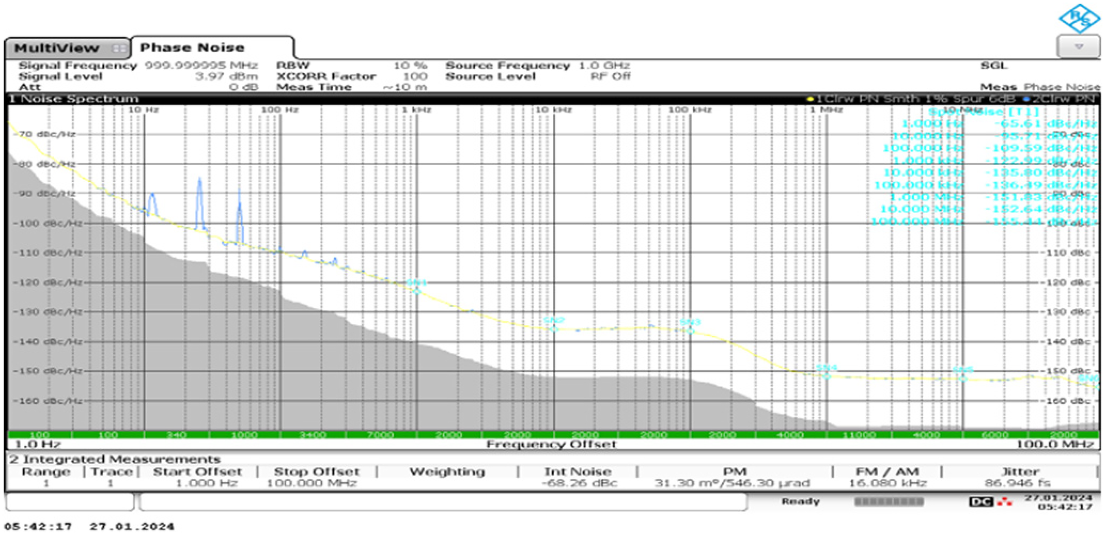
Measured phase-noise spectrum of the signal source using the FSWP50 analyzer.
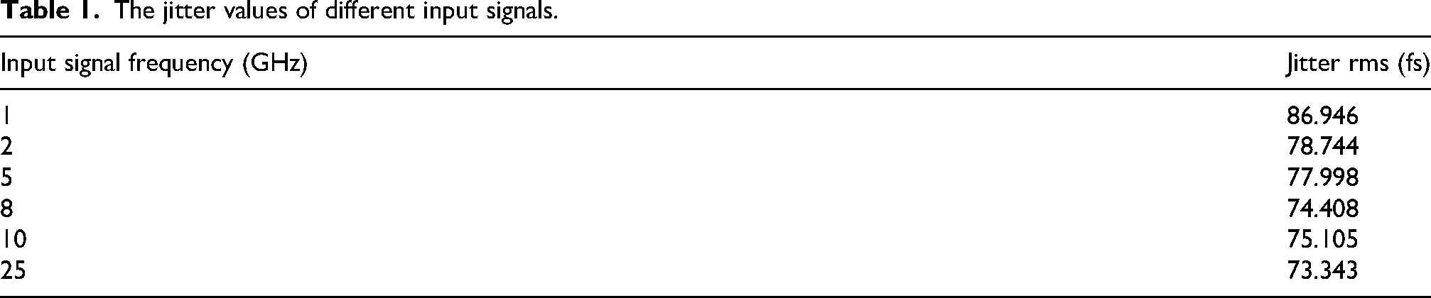
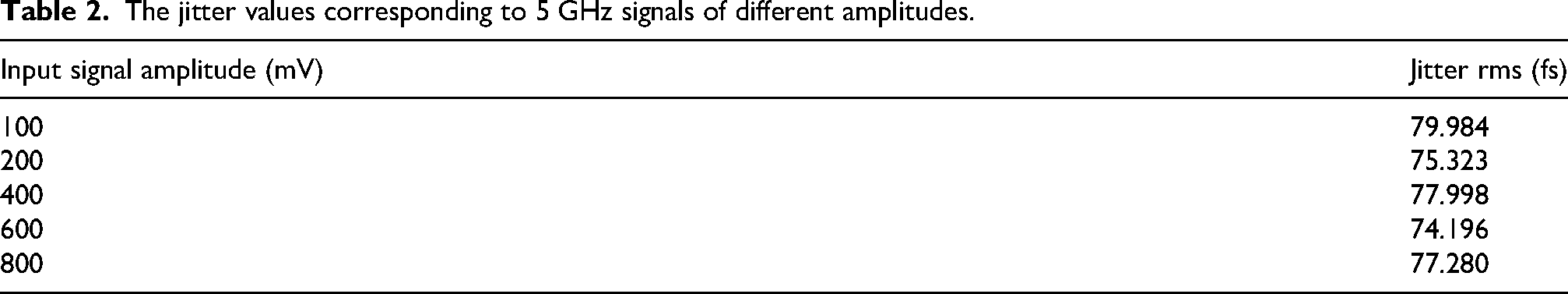
Table 1 presents the jitter values of different frequency input signals generated by the Keysight E8257D signal source measured by the FSWP50 Phase Noise Analyzer at frequency offsets ranging from 1 Hz to 100 MHz. According to the measurement results of the phase noise analyzer, the jitter of the generated 400 mV, 1 GHz sine wave signal is 86.946 fs, and this jitter decreases with the increasing signal frequency, but the overall change is very small. Table 2 summarizes the jitter results measured by the FSWP50 phase noise analyzer for an input signal at the same frequency under different amplitudes. The results show small fluctuations in the measured jitter across amplitudes; however, these variations do not exhibit a monotonic or consistent trend with amplitude, and their magnitude is limited. Therefore, under the experimental conditions and instrument settings used in this work, the observed differences are insufficient to conclude that amplitude changes cause a significant change in the signal source jitter.
The jitter values of different input signals.
The jitter values corresponding to 5 GHz signals of different amplitudes.
Building the jitter measurement floor measurement system for oscilloscopes
The technical specifications of the broadband sampling oscilloscope Keysight N1000A indicate that when the trigger signal frequency is below 4 GHz, by altering the measurement conditions, the oscilloscope achieves a minimum jitter measurement floor of less than 400 fs, approximately five times 86.946 fs. According to the literature, 17 it is known that the lower the input signal frequency is, the larger the oscilloscope's jitter measurement floor is. When the frequency of the input signal is high enough, the jitter of the signal itself is small enough, and the impact of the jitter of the input signal of any frequency generated by the signal source E8257D on Jrms can be ignored. At this time, the oscilloscope's measurement of the jitter of the signal Jrms can be approximately regarded as the oscilloscope's jitter measurement floor JMF.
In this study, a measurement system is constructed for the jitter measurement floor, as shown in Figure 5. The low-jitter measurement source, an E8257D signal source generator, is selected to provide input signals, which are connected to the input terminal of the N1000A oscilloscope. The Agilent E4438C signal source provides synchronous trigger signals connected to the trigger port of the N1000A oscilloscope to achieve external triggering. The signal sources E4438C and E8257D are connected to the 10 MHz synchronization ports on the rear panel of the instrument via a cable, enabling synchronization between the trigger signal and the input signal to reduce the jitter caused by the trigger signal. In this experiment, the frequency of the trigger signal generated by the Agilent E4438C is set to 1 GHz.
Experimental setup for measuring the oscilloscope jitter measurement floor.
The influence of different factors on the jitter measurement floor
Section 2 briefly analyzes the factors that affect the oscilloscope's jitter measurement floor. The vertical sensitivity of the oscilloscope and the amplitude of the input signal will affect the magnitude of the noise, and the final effect of the noise superimposed on the signal depends on the frequency of the input signal.
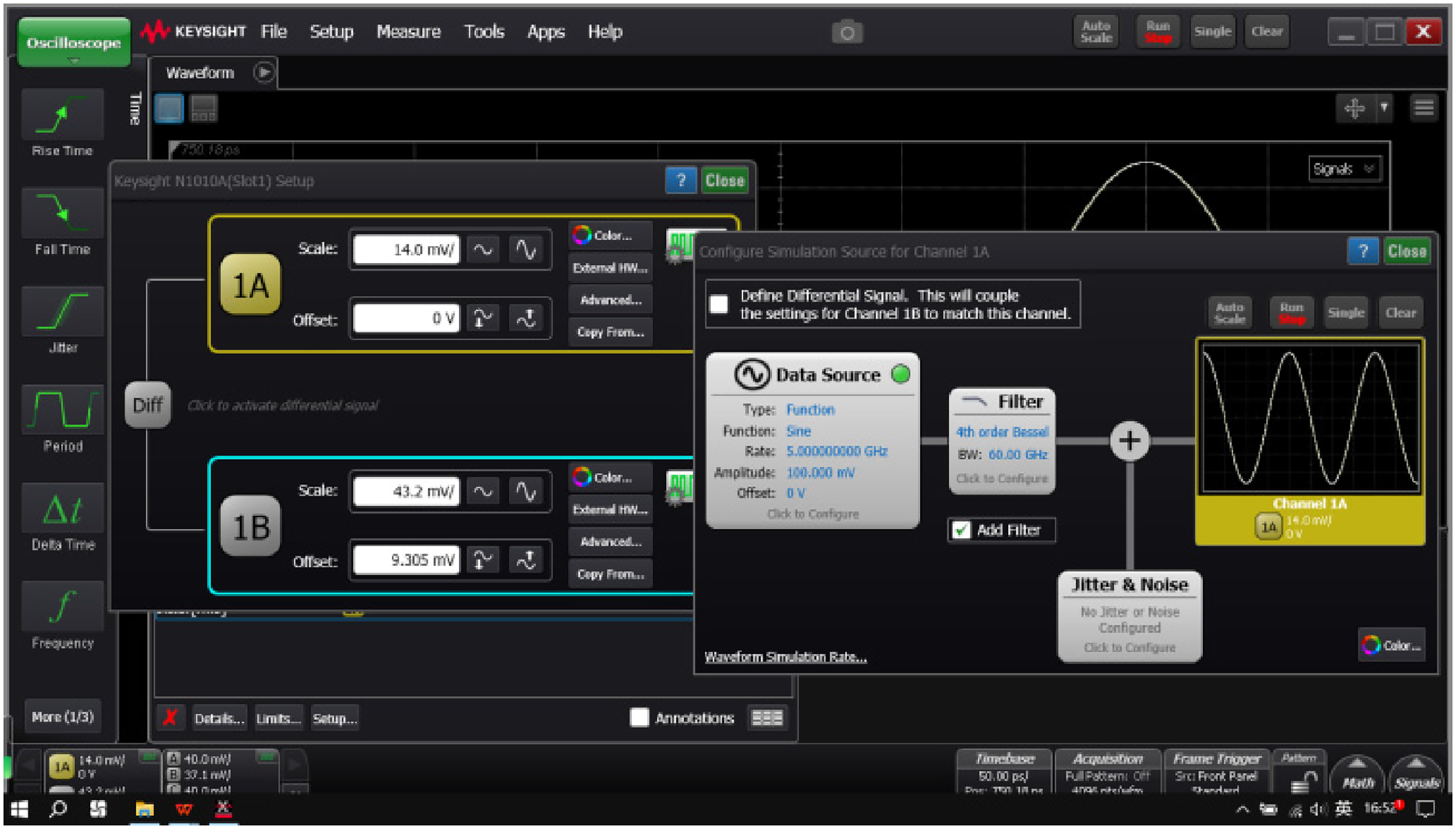
The effects of the three factors were experimentally evaluated using the measurement setup shown in Figure 6. On the premise of ensuring that the input signal is fully displayed in the broadband sampling oscilloscope, the vertical sensitivity of the sampling oscilloscope, the amplitude of the input signal and the frequency are respectively changed. The oscilloscope jitter measurements obtained under the corresponding test conditions were recorded and used as approximations of the jitter measurement floor. The jitter measurement values under the corresponding test conditions were obtained using FlexDCA. The simulation results were generated by the waveform simulation function built into FlexDCA, and the simulation procedure was configured to match the experimental measurement process. In the simulation, the input signal was generated by the software signal-source function and set as a sinusoidal waveform. The input frequency and amplitude were adjusted for different test cases, while the oscilloscope-side parameters, including vertical sensitivity and time-base settings, were configured accordingly. In addition, controllable extra jitter/noise was introduced into the input signal through the built-in Jitter & Noise module, as shown in Figure 7, and the output jitter rms value was used as the simulation result.
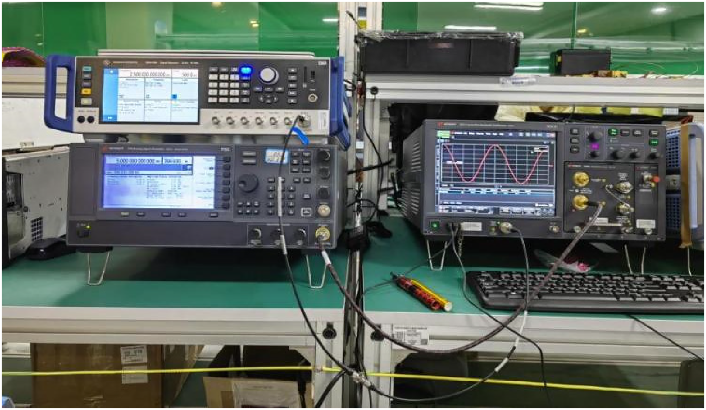
Actual measurement system.
The FlexDCA software.
The measured and simulated jitter results are summarized in the following tables.
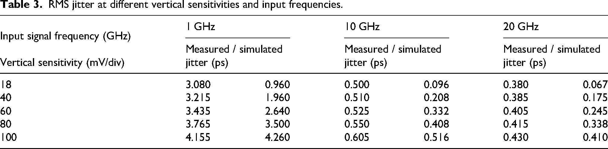
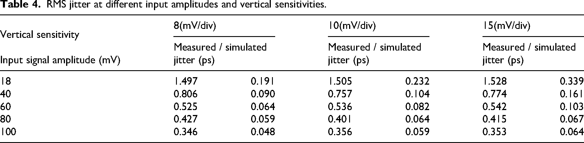
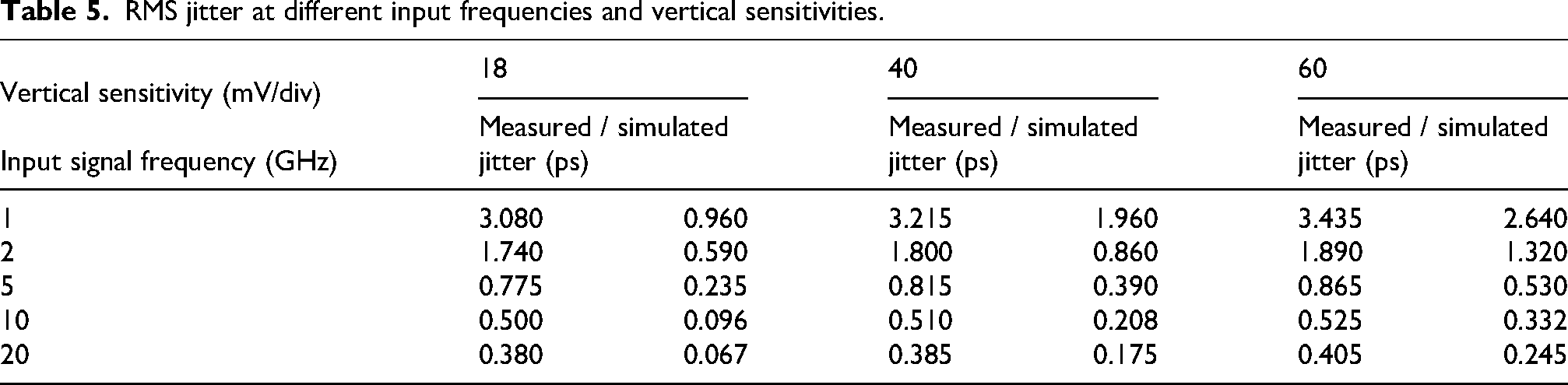
As shown in Tables 3–5, when the input signal is fully displayed on the broadband sampling oscilloscope, the measured and simulated results exhibit consistent variation trends. Specifically, the jitter measurement floor decreases with increasing vertical sensitivity, input signal amplitude, and input signal frequency. In particular, when the vertical sensitivity is changed from 100 mV/div to 18 mV/div, the measured jitter decreases by up to 25.9%; when the input amplitude increases from 18 mV to 100 mV, the measured jitter decreases by up to 76.9%; and when the input frequency increases from 1 GHz to 20 GHz, the measured jitter decreases from 3.435 ps to 0.405 ps, corresponding to a reduction of approximately 88.2%. These results indicate that, within the investigated range of this study, the input signal frequency has the most significant influence on the jitter measurement result, followed by the input signal amplitude, whereas the effect of vertical sensitivity is comparatively smaller.
RMS jitter at different vertical sensitivities and input frequencies.
RMS jitter at different input amplitudes and vertical sensitivities.
RMS jitter at different input frequencies and vertical sensitivities.
The measurement scheme for the oscilloscope jitter measurement floor
The jitter measurement floor of an oscilloscope is a parameter that varies with measurement conditions. In practical applications, the minimum value of the jitter measurement floor under specific trigger conditions is of greater interest. By leveraging the measurement system shown in Figure 6 and integrating the influencing factors analyzed in Section 3.3, a systematic methodology is established to determine the minimum jitter measurement floor by identifying optimal measurement conditions.
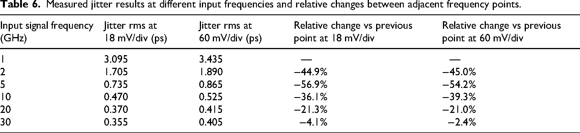
To minimize the impact of external factors such as temperature drift, measurements must be completed rapidly within a short timeframe. In this study, with the input signal amplitude fixed at 100 mV, the minimum jitter measurement floor (JMF) is investigated. As derived in Section 3.3, JMF decreases with higher vertical sensitivity. Therefore, while ensuring the input signal is fully displayed, the vertical sensitivity is minimized. Additionally, the jitter measurement floor decreases with increasing input signal frequency. To provide a quantitative basis for selecting the initial frequency in the screening procedure, the relative change in the jitter measurement floor between adjacent high-frequency points is adopted as the evaluation metric. As shown in Table 6, when the input signal frequency increases from 20 GHz to 30 GHz, the relative changes are only 4.1% at 18 mV/div and 2.4% at 60 mV/div, indicating that the reduction trend has become much less pronounced than in the lower-frequency region. Accordingly, 20 GHz is chosen as the initial input signal frequency for the subsequent measurements.
Measured jitter results at different input frequencies and relative changes between adjacent frequency points.
The measurement procedure for the Keysight N1000A oscilloscope's jitter measurement floor is illustrated in Figure 8. Since the input signal amplitude affects the measured jitter floor, the amplitude was fixed at 100 mV, while the vertical sensitivity and input frequency were adjusted to determine the minimum jitter measurement floor. This value is then compared with the nominal jitter measurement floor specified in the oscilloscope's technical specifications, thereby validating the feasibility of the proposed methodology.
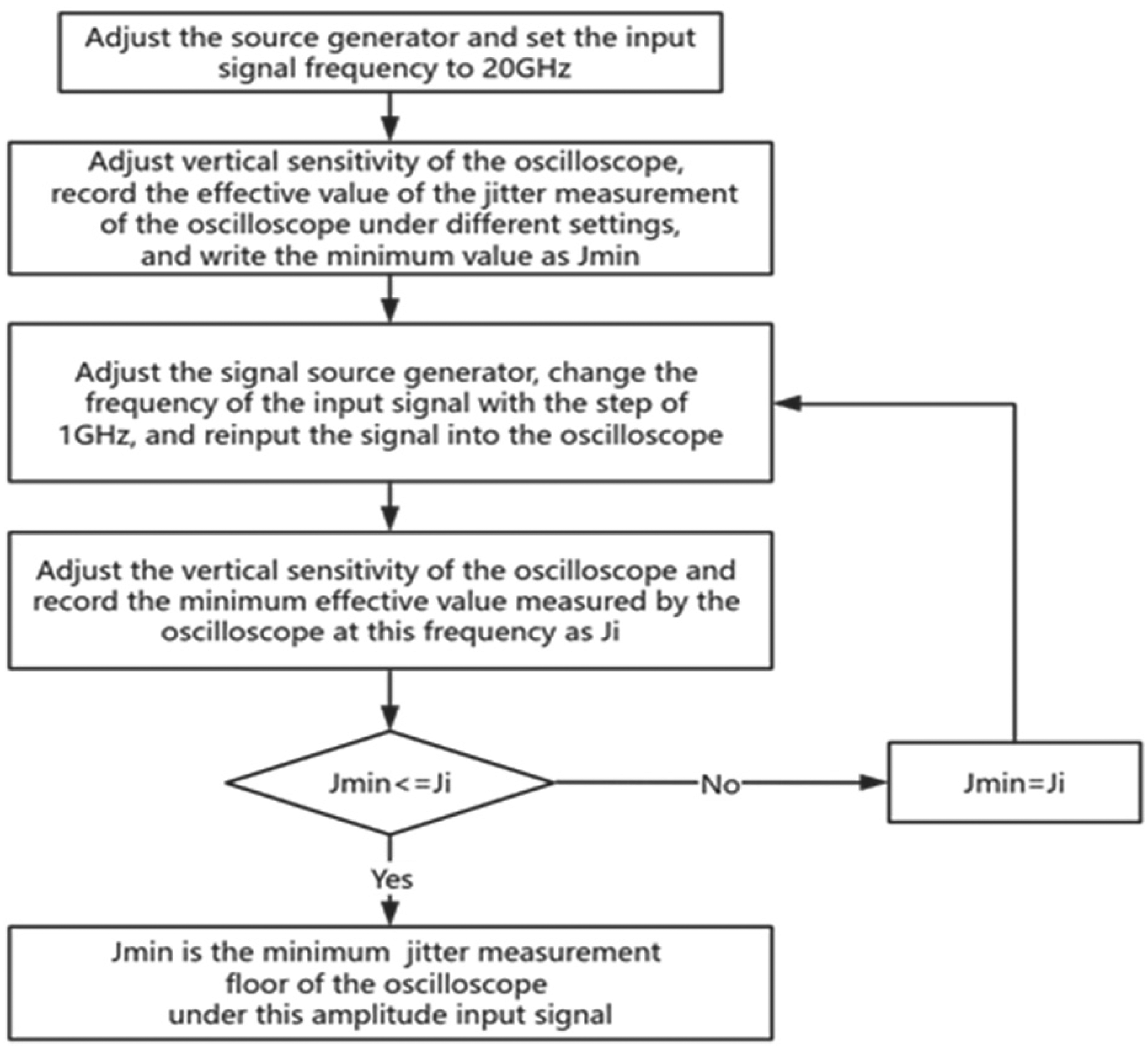
The illustration of the oscilloscope's jitter measurement floor measurement process.
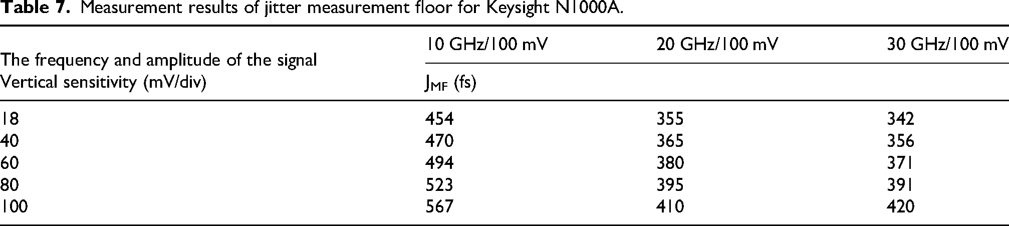
The above measurement process greatly reduces the measurement time and minimizes the influence of factors such as temperature on the measurement results. Some measurement results are shown in Table 7. According to Table 7, when the trigger signal frequency is 1 GHz and the input signal amplitude is 100 mV, the minimum jitter measurement floor of the Keysight N1000A is 342 fs. This value is consistent with the nominal jitter specification of less than 400 fs, demonstrating the feasibility of the proposed measurement scheme. It is worth noting that in this measurement scheme, the jitter of the input signal is relatively low compared to the oscilloscope jitter measurement floor. Therefore, the contribution of the jitter of the input signal to Jrms can be considered negligible.
Measurement results of jitter measurement floor for Keysight N1000A.
Analysis of the relationship among the jitter measurement floor, source jitter, and measured jitter
The measurement scheme presented in Section 3 relies on the availability of a low-jitter signal source. If such a source is unavailable, the above scheme may introduce non-negligible errors, and an alternative method is therefore needed. The root-mean-square model proposed by J. Hancock et al. provides a useful basis for developing such a method.
18
As shown in equation (2), the relationship among the measurement results Jrms obtained by the oscilloscope for signal jitter include both the input signal jitter JS and the oscilloscope's jitter measurement floor JMF satisfies the root-mean-square combination model. In this study, the input signal jitter and the oscilloscope jitter measurement floor are treated as independent under the test conditions considered. The input signal jitter mainly originates from the phase noise and timing instability of the signal source, whereas the oscilloscope jitter measurement floor is mainly associated with sampling-clock jitter, front-end noise, and internal measurement-system noise. Since these two jitter components arise from different physical sources, it is reasonable, under the conditions of this work, to treat them as uncorrelated for the purpose of analysis and parameter extraction. On this basis, this paper further examines the validity of this relationship through simulation and experiment, and explores the feasibility of extracting the jitter measurement floor without relying on a low-jitter signal source, thereby providing an alternative scheme for jitter measurement floor characterization.
Simulation verification
FlexDCA is a software platform that provides waveform-generation, jitter-analysis, and measurement-emulation functions for sampling-oscilloscope-based studies. Additionally, it can add arbitrary amounts of random jitter and noise to signals.
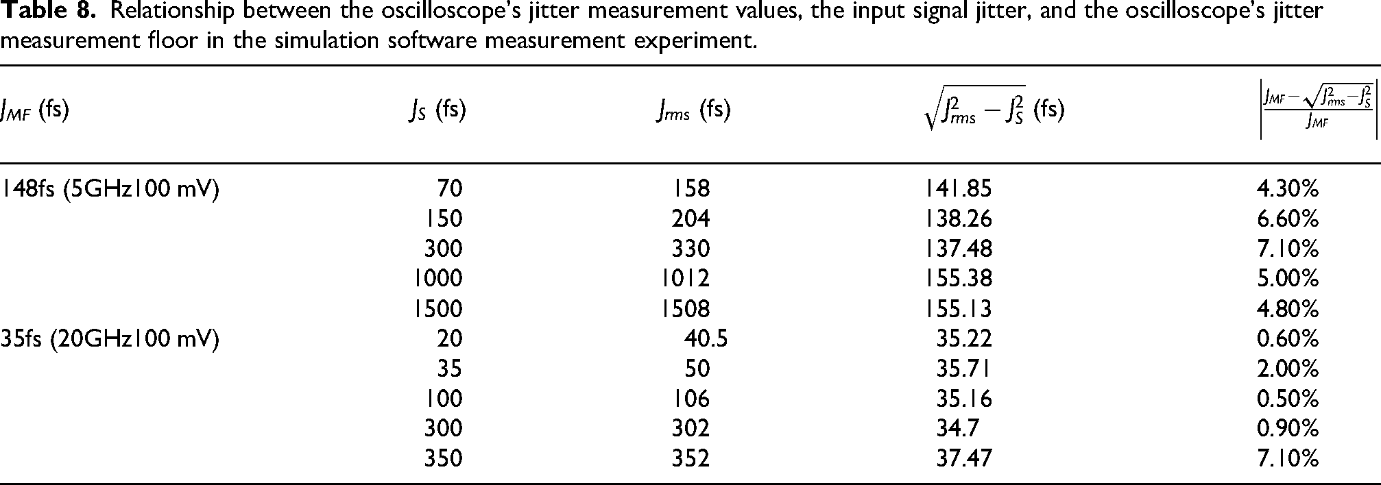
To verify the root-mean-square combination model, first, a signal input to the oscilloscope is set up without any added jitter or noise. At this point, the measurement result on the oscilloscope can be considered the oscilloscope's jitter measurement floor. Then different levels of jitter are added to the signal and the measurement results on the oscilloscope are recorded. This process is repeated multiple times while varying the amount of signal jitter, and the measurement results are recorded. According to the results displayed in Table 8, it can be observed that the relationship between these three variables conforms to the root-mean-square combination model, with the errors controlled within 10%.
Relationship between the oscilloscope's jitter measurement values, the input signal jitter, and the oscilloscope's jitter measurement floor in the simulation software measurement experiment.
Experiment verification
The experimental setup is similar to that shown in Figure 6. The Keysight E8257D vector signal generator is still used to generate the input signal, and different levels of jitter are added to the signal source utilizing the phase modulation function. The difference is that the Rohde and Schwarz SMA100B signal generator is used to provide synchronous trigger signals, with a frequency of 2.5 GHz and an amplitude of 500 mV. The Keysight N1000A is still used as the oscilloscope being tested, and the Rohde and Schwarz FSWP50 phase noise analyzer is used to measure the jitter of the signal source. The schematic diagram of the actual equipment connection is shown in Figure 9.
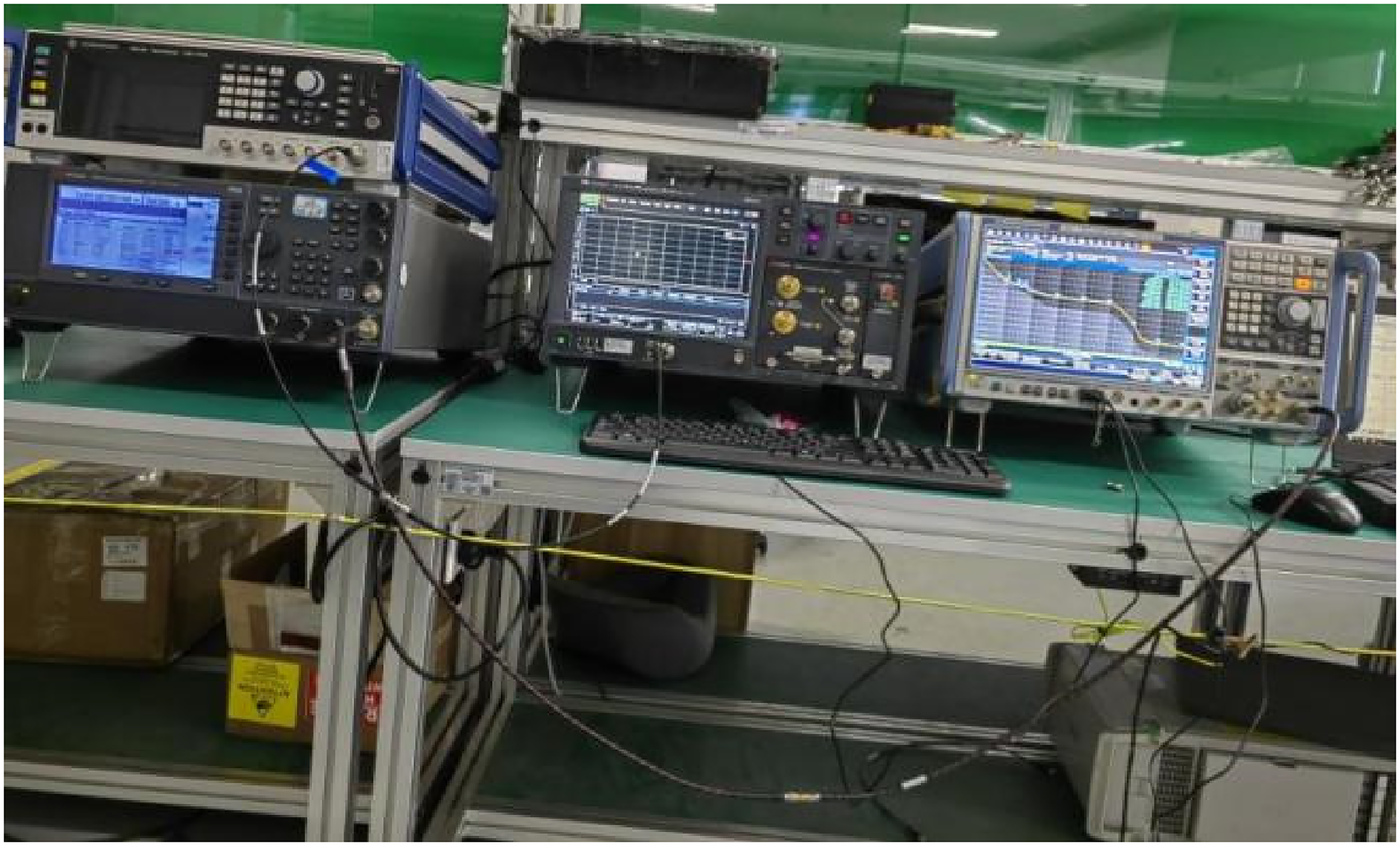
Diagram of equipment connections.
First, the signal source generator E8257D is adjusted to produce a low-jitter signal input to the oscilloscope. The oscilloscope's measured result Jrms is recorded under this measurement condition and considered the jitter measurement floor JMF. Then, while keeping the other measurement conditions constant, the E8257D signal source generator is adjusted to add Gaussian noise of different magnitudes to the input signal through phase modulation, thereby changing the jitter value of the input signal. The oscilloscope's measured result Jrms is recorded under these conditions. Each time the input signal jitter is changed, the signal needs to be connected to the phase noise analyzer to record the signal jitter JS. The specific measurement and calculation data can be found in Table 9.
Relationship between the measured jitter values of the oscilloscope, the jitter of the input signal, and the oscilloscope jitter measurement floor in the experimental measurement.
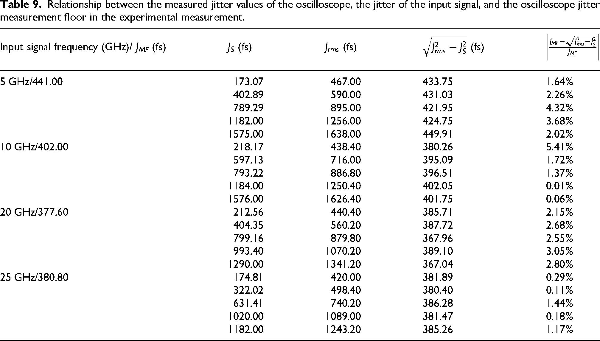
According to Table 9, it can be observed that regardless of whether the jitter of the input signal is several times larger, several times smaller, or even substantially larger than the oscilloscope jitter measurement floor, the jitter values all fall within a 6% error range, satisfying the root-mean-square combination model.
Measurement scheme for the oscilloscope's jitter measurement floor
The measurement method in Section 3 requires certain specifications for the signal source, which needs to have a sufficiently low jitter. According to the analysis in this section, the relationship between the oscilloscope's jitter measurement floor JMF, the signal jitter JS, and the oscilloscope's jitter measurement value Jrms conforms to equation (2). Therefore, based on this relationship, a reconstructed measurement scheme is proposed for cases in which no low-jitter source is available. The specific measurement system and calculation process are shown in Figure 10.
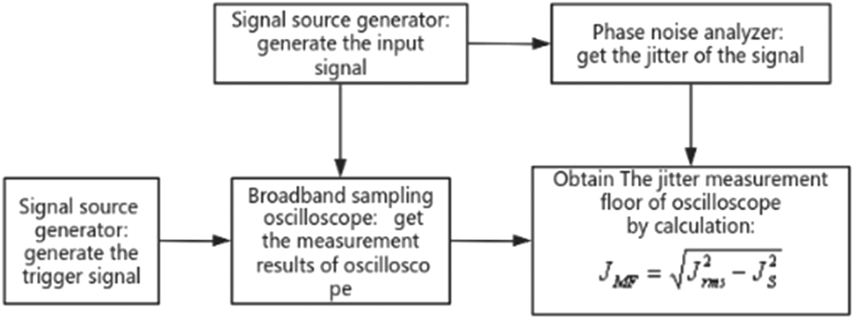
Measurement and calculation process flowchart of jitter measurement floor.
The Keysight E8257D vector signal generator was used to generate the input signal, while the Rohde and Schwarz SMA100B signal generator was used to provide the synchronous trigger signal with a frequency of 2.5 GHz and an amplitude of 500 mV. The Keysight N1000A broadband sampling oscilloscope was used as the instrument under test, and the Rohde and Schwarz FSWP50 phase noise analyzer was used to measure the jitter of the signal source. It should be noted that the extracted jitter measurement floor may be affected by factors such as the phase-noise measurement accuracy, the selected integration range, the vertical sensitivity setting, the input signal frequency, the trigger condition, connection repeatability, and environmental fluctuations. Therefore, the experiment should be carried out under stable and consistent test conditions. Within the scope of this study, the combined influence of these factors remains acceptable and does not affect the validity of the conclusions.
To reduce random fluctuations and improve result repeatability, the oscilloscope jitter result Jrms under each measurement condition was determined as the average of five repeated measurements. In addition, to verify that the proposed method does not rely on the availability of a low-jitter signal source, the input signal jitter was varied over several levels while keeping the other measurement conditions unchanged, and multiple sets of oscilloscope data were collected for subsequent analysis (Table 10).
The measurement and calculation results of multiple sets of data obtained under input signals of different frequencies.
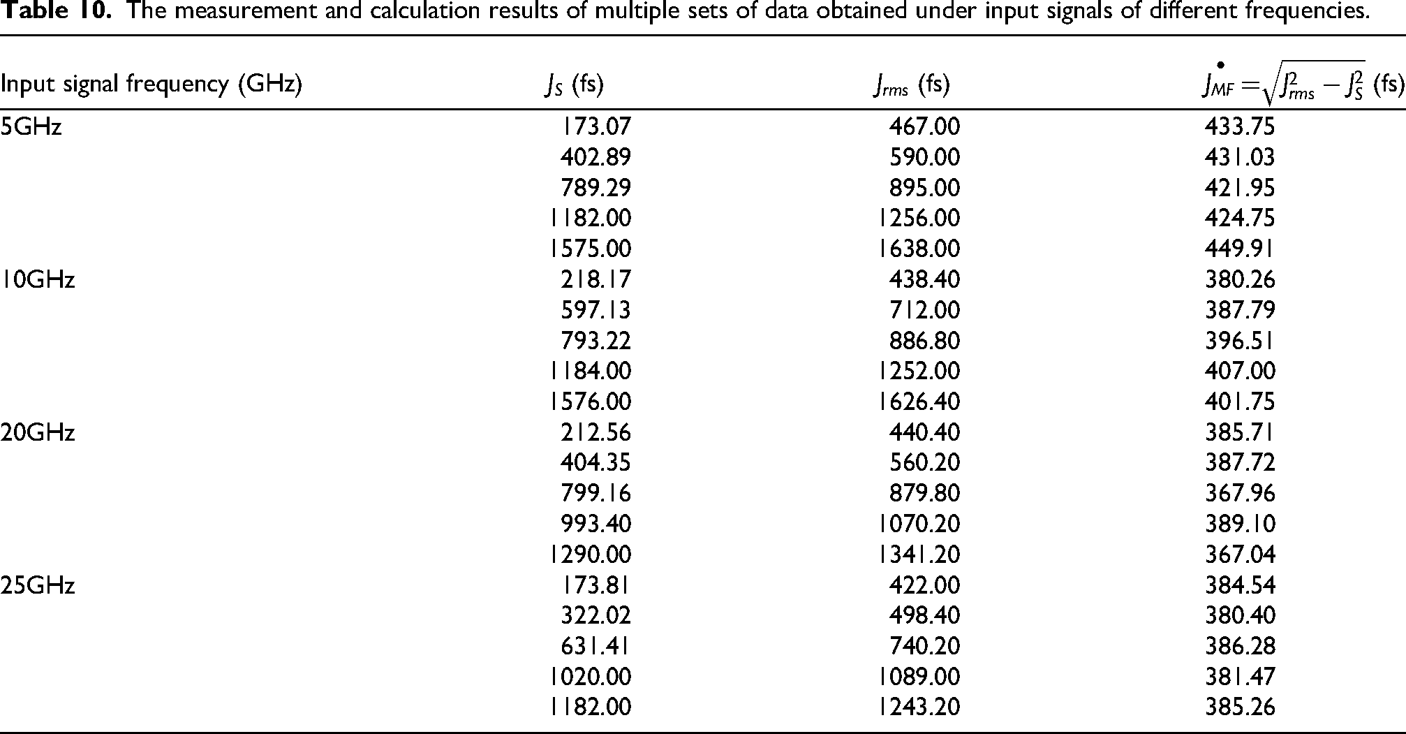
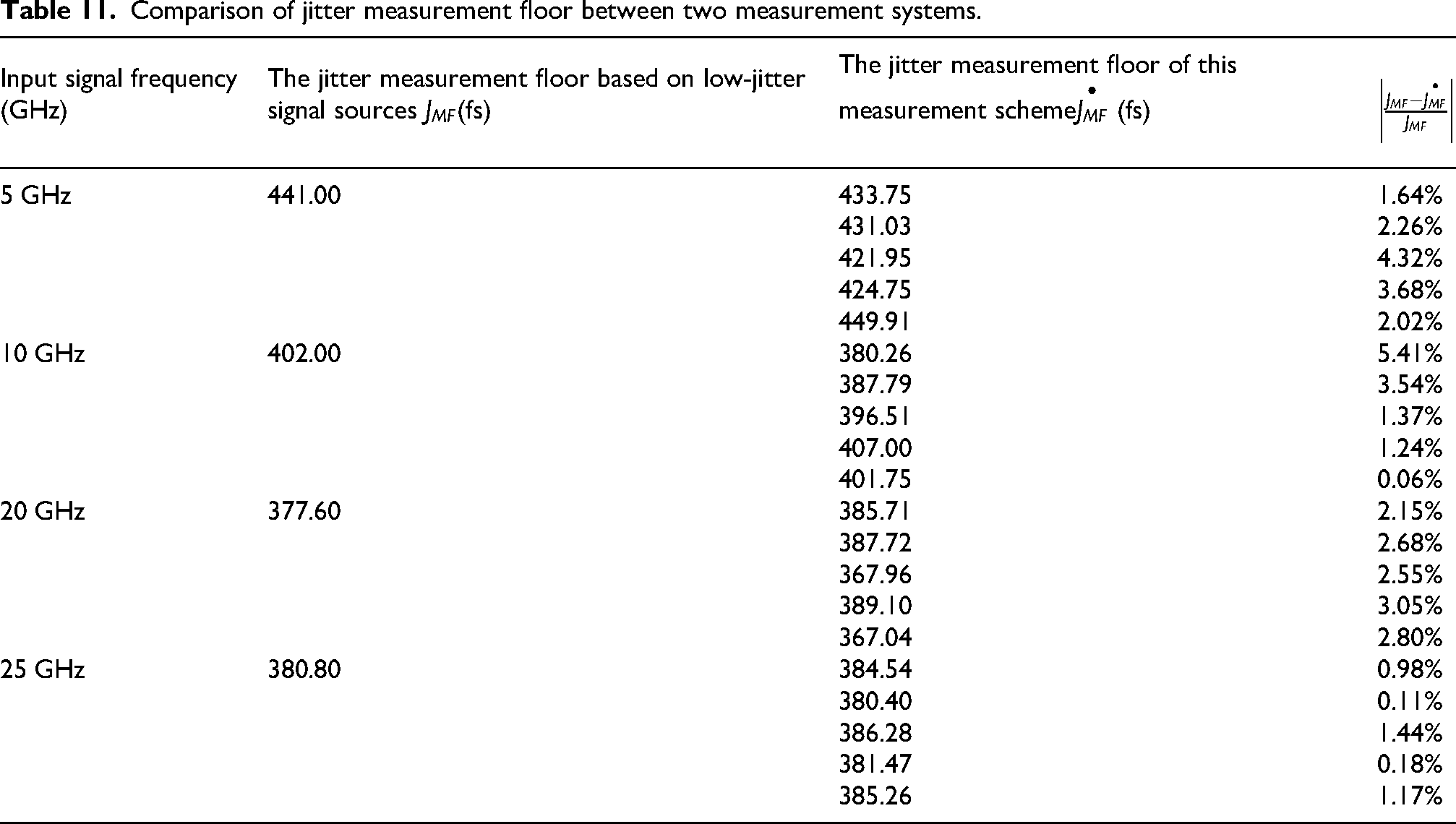
Table 11 presents a direct comparison between the proposed method and the conventional low-jitter-source approximation for extracting the oscilloscope jitter measurement floor JMF under the same test conditions. At 5, 10, 20, and 25 GHz, the two methods give highly consistent JMF results, with relative deviations ranging from approximately 0.06% to 5.41%, indicating that, within the scope of this study, the proposed method has good comparability with the conventional method in terms of extraction accuracy. For the broadband sampling-oscilloscope jitter-floor evaluation considered in this work, this level of deviation is acceptable for engineering comparison and parameter extraction.
Comparison of jitter measurement floor between two measurement systems.
Compared with the conventional approximation, which relies on the prerequisite JS≪ JMF , the proposed method uses the root-mean-square relationship among Jrms, JS, and JMF to achieve reliable extraction of JMF even when an ultra-low-jitter source is unavailable, thereby reducing the dependence of the measurement system on ultra-low-jitter signal sources. In addition, the calculation process of the proposed method is relatively straightforward, making it easier to integrate into existing test workflows. It should be noted that the effectiveness of the proposed method still depends on the reasonable measurement and estimation of JS; when the phase-noise measurement accuracy is insufficient, the integration range is improperly selected, or strong correlated noise exists in the system, the extracted results may be affected.
Conclusions
This study investigated the characterization and extraction of the jitter measurement floor of broadband sampling oscilloscopes. The effects of vertical sensitivity, input signal frequency, and input signal amplitude on the jitter measurement floor were systematically analyzed, and a rapid screening procedure together with an RMS-based extraction method was proposed. Experimental results show that, under a 1 GHz external trigger condition, the minimum jitter measurement floor measured for the Keysight N1000A broadband sampling oscilloscope was 342 fs, satisfying the specification of less than 400 fs in its datasheet. In addition, the relative deviation remains within 6%, indicating acceptable extraction accuracy for engineering applications. The proposed rapid screening procedure can reduce the trial-and-error involved in test parameter adjustment and improve the efficiency of jitter measurement floor evaluation. Moreover, when an ideal ultra-low-jitter signal source is unavailable, the proposed method still provides a feasible approach for evaluating the jitter measurement floor of broadband sampling oscilloscopes and can be conveniently incorporated into existing test workflows.
The present study verifies the proposed method under the tested experimental conditions. Nevertheless, the extracted results may still be influenced by uncertainty in signal-jitter estimation, instrument residual noise, integration-range selection, environmental drift, and connection repeatability. Future work will investigate long-term stability, broader operating conditions, and the quantitative contribution of individual uncertainty sources.
Footnotes
Acknowledgements
This study is supported by “Broadband Sampling Oscilloscope” on National Key Research and Development Program of “Fundamental Research Conditions and Development Program of Major Scientific Instruments” (No.2022YFF0707104).
Ethical considerations
This article does not contain any studies with human or animal participants.
Consent to participate
There are no human participants in this article and informed consent is not required.
Consent for publication
There are no human participants in this article and informed consent is not required.
Funding
The authors disclosed receipt of the following financial support for the research, authorship, and/or publication of this article: This work was supported by the National Key Research and Development Program of China, (grant number No.2022YFF0707104).
Declaration of conflicting interests
The authors declared no potential conflicts of interest with respect to the research, authorship, and/or publication of this article.
Data availability
Data can be obtained from the corresponding author upon request.