






Abstract
In the quest for increased student understanding of the principles underlying high-frequency response of Field Effect Transistor amplifiers, a laboratory exercise employing a unique method to determine the intrinsic transistor model capacitances was used. The method employs two simple measurements: determination of the high 3-dB frequency for a common-source amplifier being driven by a Thévenin source with two different output resistance values. Circuit simulation results utilizing these experimentally determined intrinsic capacitances show much greater correlation to experimental results than those typically obtained using manufacturer-supplied values. Students participating in the laboratory exercise reported good gains in knowledge levels and reasonable gains in confidence levels.
Introduction
Electrical engineering programs strive to closely link hand calculations, computer simulation, and experimental results in the analysis and design of transistor amplifiers. This linkage is typically accomplished in laboratory portions of electronics courses using well-known conversions between manufacturer-supplied data, either from data sheets or SPICE parameters, and hand calculation parameters. 1 Low-frequency models can be improved over manufacturer-supplied data through the use of a transistor curve tracer to determine model parameters for individual transistors. Using such modified models leads to good correlations in amplifier quiescent conditions and low-frequency performance.
At high frequencies, however, determination of model parameters is problematic. In the case of both Bipolar Junction Transistors (BJTs) and Field Effect Transistors (FETs), high-frequency performance is modeled by capacitors connected between nodes of the transistor model. Several methods have been proposed for measuring these capacitance parameters.2,3 Unfortunately, some methods propose etching materials from a semiconductor structure and are not practical in a typical instructional electronics laboratory setting.
In addition, the typical breadboard used in instructional laboratories may introduce significant stray capacitance in the circuit, increasing the variation between experimental results and those obtained by analytic or simulation techniques. In general, this variation can be detrimental to student confidence and learning. Students often seem to feel that either the models failed or that the parameters supplied by manufacturers are overly optimistic.
A simple laboratory exercise that would allow students to determine transistor model capacitance parameters experimentally was explored. In order to verify the model, analytic, simulation, and experimental results are compared. The course instructors assessed whether this exercise increased student knowledge concerning high-frequency modeling of transistors and their confidence in using those models to predict amplifier performance.
Theoretical background
The hybrid-π, small-signal, high-frequency model of a FET is shown in Figure 1. The high-frequency behavior of the FET is modeled though the two capacitors, Cgs and Cgd. Good approximations of those intrinsic FET capacitor values must be obtained in order to have accurate modeling of transistor high-frequency performance. While the technique used is applicable to both BJTs and FETs, it was decided to use a JFET for this first effort. The decision was based primarily on the well-known JFET transformations of model capacitors to SPICE parameters.
1
A depletion MOSFET would be another good choice: the transformations for enhancement MOSFETs are more complicated and BJTs suffer the dilemma of converting the two model capacitors into the three SPICE parameters used to describe high-frequency effects.
FET small-signal model.
Summary of Field Effect Transistor (FET) common-source pole frequencies.
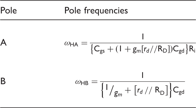
Of particular significance to the development of the laboratory exercise is that pole A (as described by ωHA) is highly dependent on the signal source output resistance, Ri (the parallel combination of biasing resistors and the signal source output resistance in the circuits of Figure 2), while pole B (as described by ωHB) is independent of the signal source output resistance. That dependence-independence relationship of the poles is such that pole A is dominant when the signal source output resistance is sufficiently large and pole B is dominant when the signal source output resistance is sufficiently small.
Two high-frequency 3-dB test circuits. (a) High signal-source output resistance. (b) Low signal-source output resistance.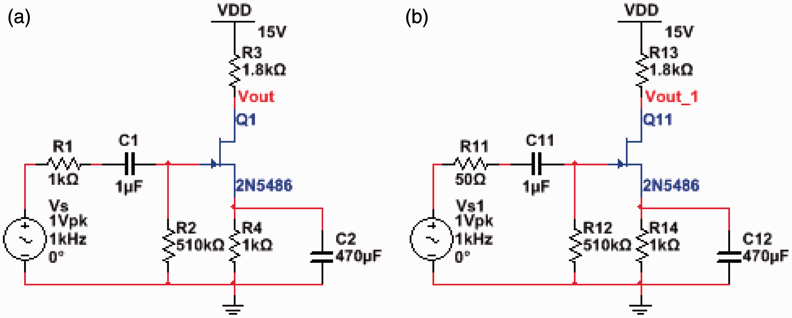
The experiment described in this article, developed by Kim and Schubert, 10 takes advantage of the switching of dominant poles with signal source output resistance in order to easily calculate the transistor model capacitors, Cgs and Cgd. The high 3-dB frequency of a single amplifier driven by two different signal sources is measured: once with a low output resistance (typically the 50 Ω output resistance of a function generator) and once with a resistor inserted between the signal source and the amplifier. Kim and Schubert then directly compute Cgd from the high 3-dB frequency for the low output resistance case and, using that value of Cgd, they compute Cgs from the high 3-dB frequency for the high-output resistance case. After the intrinsic capacitor values are calculated from the measured dominant pole test circuits using simple dominant pole analysis, SPICE models are back-calculated using the standard expressions for converting small-signal model capacitors to the capacitance parameters used in the SPICE models.
The laboratory exercise
The students participating in this laboratory exercise were typically in their second semester of a two-semester, junior-level electronics course. In the first semester, they became familiar with low-frequency analysis, modeling, simulation, and experimental testing of both BJT and FET amplifiers. Prior to this laboratory exercise, the students had received instruction and homework exercises in high-frequency performance of single-transistor BJT and FET amplifiers. The instruction included the derivation of high-frequency amplifier pole frequencies.
In the laboratory, the students were given a 2N5486 JFET (arbitrarily chosen) and asked to determine the DC characteristic parameters of that transistor (IDSS, VPO, and VA) using a transistor curve tracer and appropriate calculations. The students had performed these measurements several times previously in other laboratory exercises, so a MathCAD template was provided to assist in the calculations and save time.
Students were directed to build the circuit of Figure 2(a) and determine its high 3-dB frequency using realistic values for the coupling and bypass capacitors. A previous experiment had explored the effect of coupling and bypass capacitors on the low 3-dB frequency and students were expected to use that information in choosing appropriate capacitor values. The circuit was then altered to become Figure 2(b) by reducing the source output resistance: R1 in Figure 2(a) (1 kΩ) was changed to become R11 in Figure 2(b) (50 Ω) – no other changes to the circuit were made.
Students were reminded that it is important that the poles be dominant poles: the signal source output resistance values must be chosen so that the high 3-dB frequencies for the two circuits differ by at least a factor of four. From the results of these two experiments, students determined the JFET model capacitance parameters Cgs and Cgd for the JFET as biased in these two circuits. Again, a MathCAD template was provided to assist in the calculations and save time. From the values obtained above and the bias conditions for the FET, the SPICE parameters CGD and CGS were calculated under the typical SPICE-parameter assumption that PB = 0.6 and M = 0.5.
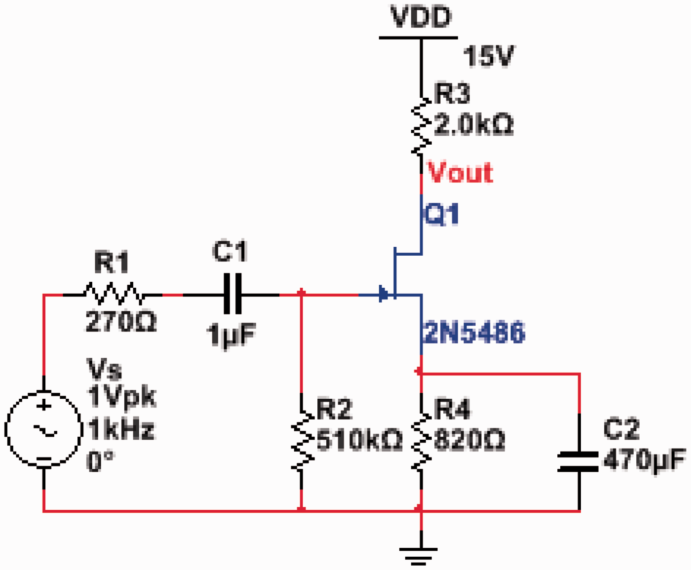
Finally students were asked to build the circuit of Figure 3 (again, using realistic values for the bypass and coupling capacitors). While this circuit is a similar common-source amplifier, the quiescent conditions for the JFET, as well as the various resistor values, are somewhat different. Students were to compare experimental DC and AC performance to Multisim™ (the SPICE-based simulator available to the students) simulations which used:
the Multisim™ model for the 2N5486 (unaltered); the Multisim™ virtual model modified to reflect the JFET parameters determined in this experiment. A test JFET circuit.
Comments on the differences/similarities in the results were recorded. In order to cancel out any oscilloscope probe frequency effects, students used the same type of probe for both input and output measurements.
Experimental observations
DC JFET parameters.
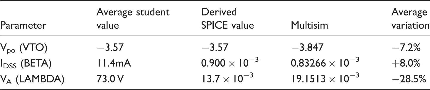
From the quiescent conditions of the circuits of Figure 2 (both circuits have the same quiescent conditions and consequently the same JFET model parameters), students determined the necessary transistor small-signal parameters using standard relationships. 1
The student experimental high 3-dB frequencies for the two source output resistance cases were quite consistent (a standard deviation of about 1/20 of a decade in each case)
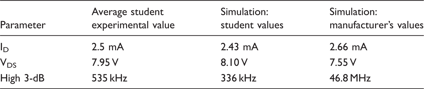
However, Multisim™ SPICE simulation using the manufacturer-supplied capacitance values for the 2N5486 JFET produces high 3-dB frequencies of 98.96 MHz and 21.0 MHz for the low and high output resistance cases. These values are about 2.2 decades higher than the student experimental results. Such large discrepancies between simulation and experiment are troubling for students.
Students then calculated the two intrinsic JFET model capacitor values using their experimental high 3-dB frequencies determined from each of the two circuits of Figure 2
From those JFET model capacitor values, the SPICE model parameters were then calculated using the bias conditions and standard transformations
1
If the above-stated average student values are used, the intrinsic capacitor values are Cgd = 108.6 pF and Cgs = 531.1 pF. These values can be converted to the SPICE parameters CGD = 483.6pF and CGS = 1.117nF. Placing these values into Multisim™ for the two circuits results in high 3-dB frequencies of fH(50 Ω) = 718 kHz and fH(1kΩ) = 124 kHz. Each of these values is within 1/30 of a decade of the experimental value and shows good correlation between practice and the model.
Comparison of simulation predictions and average experimental results.
From the instructor viewpoint, the experiment went smoothly with a few areas for improvement. Some students misunderstood the instruction to use “realistic values for the coupling and bypass capacitors” when building their test circuits. The instructions have been modified to ensure that the capacitor bypassing the resistor connected to the FET source terminal is sufficiently large so that it effectively shorts that resistor at frequencies well below the high 3-dB frequency. Modeling the high-frequency performance of the transistor is sensitive to accurate measurements of the high 3-dB frequency. It is vital that the function generator used is capable of high-quality sine waves at the high 3-dB frequencies measured, and that students make sure that the input signal is of appropriate magnitude so that the transistor amplifier is operating in its linear region. Linearity can be easily determined with an “x–y” plot on the oscilloscope of the input–output relationship at midband frequencies.
It should also be noted that the two necessary signal source resistance values used in this experiment can vary with transistor and circuit element values. When designing this experiment using different transistors or circuit elements, the resistance values chosen should be alternately larger and smaller than the dominant-pole crossover resistance value (the value where ωHA = ωHB)
A simple voltage divider can be used, if necessary, to lower the apparent output resistance of the signal source (typically 50 Ω).
Assessment of student knowledge and confidence
One of the aims of this study was to assess student learning in the laboratory concerning frequency response and simulation of transistor circuits. Specifically:
Does this methodology increase basic understanding of transistor amplifier and design tools? Does student confidence in applying the concepts learned increase?
Short questionnaires were designed to provide insight into the student level of knowledge concerning amplifier circuits and their confidence in applying that material. Just prior to beginning the laboratory exercise, students were asked to score (on a scale from 1 to 5) their prior knowledge. To provide further insight into actual student knowledge level, students were asked to respond with a short answer to the knowledge queries. After the exercise was completed, the questionnaires were again completed by the students and the post-exercise written responses scored by the investigators to measure changes in knowledge level. In order to track individual student incremental changes, students submitted the surveys together at the end of the exercise. All surveys were submitted without any identifying markers so that student anonymity would be preserved. The use of student-assigned scores to assess gains in student knowledge and confidence has been successfully used by the investigator team in previous studies.11,12
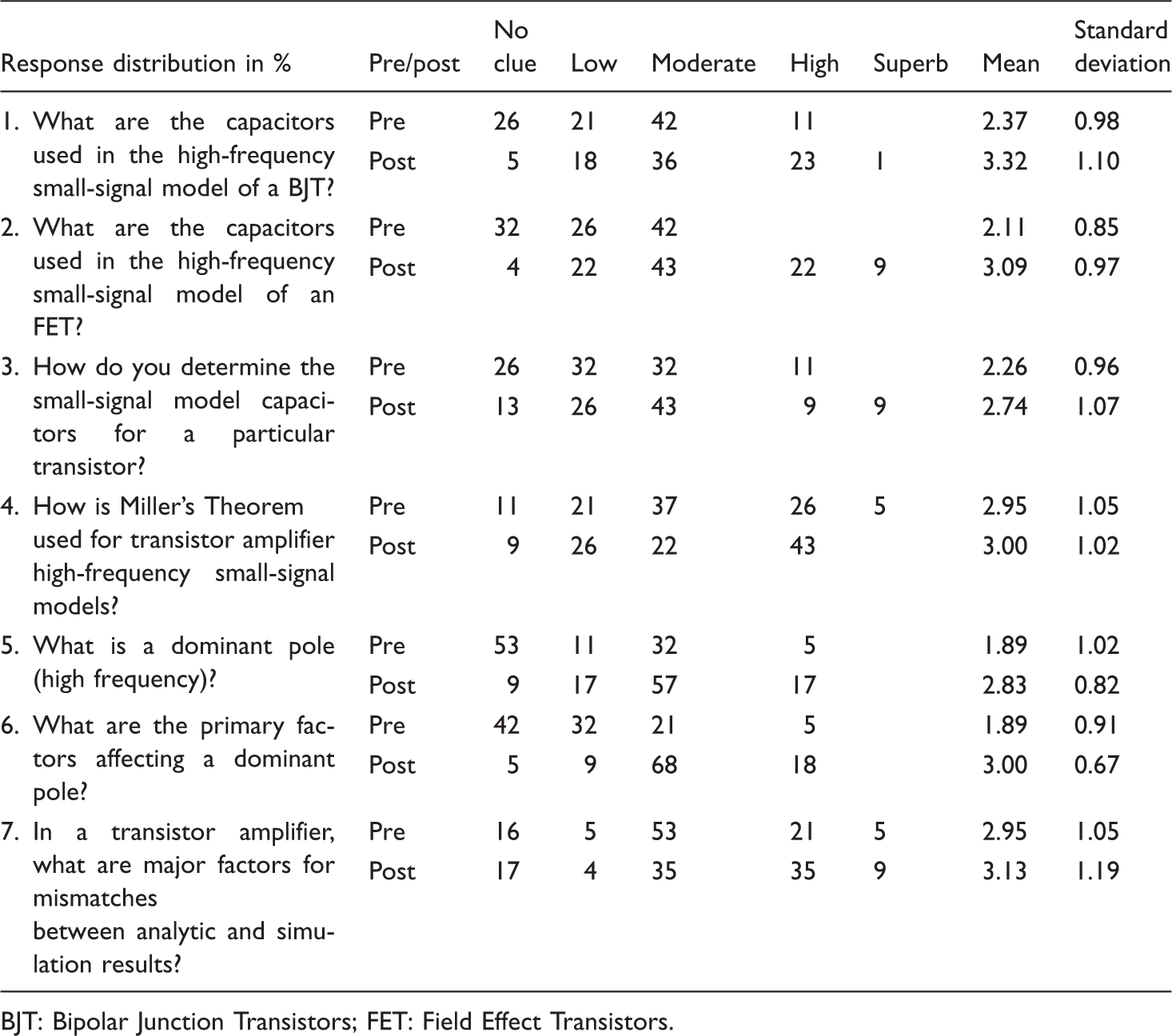
The following seven queries concerning knowledge concerning transistor capacitance modeling were asked before and after the laboratory exercise.
What are the capacitors used in the high-frequency small-signal model of Bipolar Junction Transistors (BJTs)? What are the capacitors used in the high-frequency small-signal model of Field Effect Transistors (FETs)? How do you determine the small-signal model capacitors for a particular transistor? How is Miller's Theorem used (in words) for transistor amplifier high-frequency small-signal models? What is a dominant pole (high frequency)? What are the primary factors affecting a dominant pole? In a transistor amplifier, what are some of the major factors contributing to mismatches between analytic and computer simulation results?
The knowledge score was based on the following scale.
1 = No clue, this concept is new to me. 2 = Low, I have only heard about the concept. 3 = Moderate, I know about the concept, but have not applied it. 4 = High, I know the concept and have tried it. 5 = Superb, I know the concept and have successfully applied it.
Knowledge survey response distribution.
BJT: Bipolar Junction Transistors; FET: Field Effect Transistors.
Student responses to queries 3, 4, and 7 showed smaller average gains in reported knowledge. Query 3 (determination of capacitance values) showed an average gain of 0.47 levels with 47.4% of the students reporting an increase in knowledge. Queries 4 (use of Miller's theorem) and 7 (sources of mismatch) reported average gains of 0.06 and 0.11 levels, respectively, with 21.1% and 36.8% of the students reporting gains, respectively.
Another portion of the questionnaire was designed to assess student confidence in applying this methodology. The following nine queries were asked before and after the exercise was performed in order to assess student confidence.
I can design transistor amplifier circuits. I can apply Miller's Theorem to create small signal models of electronic circuits. I can perform high-frequency small-signal analysis of analog electronic circuits I can determine circuit high-frequency dominant poles. I can use computer simulation tools for analyzing electronic circuits. I can use a circuit simulation tool to alter transistor model parameters. I can convert between the transistor parameters used in analytic models and those used in circuit simulation models. I can compare high-frequency cut-off calculations for transistor amplifiers circuits and verify performance characteristics using computer simulation. I can reconcile mismatches between analytic and simulation high-frequency cut-off results.
The confidence score was based on the following scale.
1 = No clue, I have no idea if I can apply the concept. 2 = Low, I have heard of the concept, but have little confidence that I can apply it. 3 = Moderate, I think I understand the concept, but am unsure about applying it. 4 = High, I am fairly sure I understand the concept and am fairly sure I can apply it. 5 = Superb, I am very confident that I understand the concept and can apply it to a new problem.
Confidence survey response distribution.
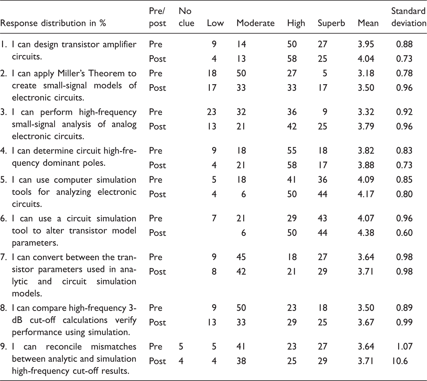
Three of the confidence queries (2, 3, and 6) experienced gains in student confidence greater than 0.3 levels and four of the queries (2, 3, 6, and 7) had more than 27% of the students reporting increases in their confidence.
Summary
The development of a meaningful student laboratory experience in transistor amplifier frequency response with a closed loop approach for finding intrinsic transistor capacitor values using SPICE and circuit analysis met its goals. Good correspondence between simulation results and model parameter calculations were achieved. In addition, students reported good increases in knowledge concerning the subjects covered and positive increases in confidence in applying the methodology covered.
Footnotes
Acknowledgement
USD Institutional Review Board approval for this project was obtained for the 2012–2013 academic year.
Conflict of interest
None declared.
Funding
This research received no specific grant from any funding agency in the public, commercial, or not-for-profit sectors.