
Abstract
In a period of rapid adaptation to technology in today’s world, limiting education to traditional methods leads to a rapid decline in the perception and interest of the learner. Augmented Reality (AR), which is among the most interesting technological innovation of the last years, are manifested in many sectors. It is used more widely in the field of education thanks to its superior advantages such as being portable, adapting to different devices/equipment, offering interactive digital content and arousing interest. In this study, AR application has been realized for the modeling of N-type MOSFET element, which is one of the basic courses of Electrical and Electronic Engineering and is widely used in analog and digital circuits. The contribution of the application to students’ perception of theoretical concepts was also examined. It concluded that AR made an important contribution to the concretization of abstract concepts and the developed educational material increased the motivation of the students.
Introduction
The question of how educational institutions will adapt to the transition from the industrial age to the digital age is of great importance. It is inevitable to reflect this transition process in social life to the field of education. In particular, the adaptation of the higher education institutions, and the instructor staff in these institutions will provide a more effective and healthy communication with the young generation who are adapting to this process rapidly and directly. For this reason, it is necessary to investigate closely how the technologies can be adapted to the field of education by following the technological developments and studies performed throughout the world. 1
Looking at the statistical data, it is possible to say that mobile devices are entering the lives of more people and internet-based usage is becoming more widespread. It is not difficult to predict that the technology used by more than half of the world's population will be offered to undergraduate students as well. Therefore, the development of educational content that can be used with mobile devices (smartphones, tablets) in institutions providing undergraduate level education will be a very effective method to keep pace with the rapid development of digital age. 2
The applications of Augmented Reality (AR) and Virtual Reality (VR) are amongst the most popular in the field of mobile technology. Research has shown that a total investment of $3 billion in 2017 (more than $1.5 billion in the fourth quarter of 2017 alone) is spent on developing AR and VR applications. 3
AR applications in education are preferred due to its advantages such as comprehending the structures that we have no chance to observe the internal structure of, and the opportunity to watch the content of the 2D course in 3D. Many studies show that AR technology has a high potential to become a standard educational tool thanks to its advantages and contributions in terms of learning in the technology age.
In the field of Electrical and Electronics Engineering, it is very important to fully understand the operating principles and electrical interactions of the circuit elements used in order to understand the working principles of analog/digital circuits. However, it is not possible to observe electron movements within the circuit elements in existing laboratory environments. Simulating electron movements that are difficult to understand in simple terms will make it easier to understand the working principles of circuit elements. 4
In this study, AR application has been realized for the modeling of N channel MOSFET (NMOS) element, which is a type of MOSFET (Metal Oxide Semiconductor Field Effect Transistor) transistor, which is widely used in analog and digital circuits in the field of Electrical and Electronics Engineering. At the same time, the contribution of the application in the perception of theoretical concepts was examined. The AR application was tested on the 2nd and 3rd year students who have completed or are continuing NMOS training and who are knowledgeable about semiconductors.
The current study focuses on students' views on AR technology through the NMOS application. In light of the above, Section 2 introduces the AR technology. The educational usage of AR technology is given in Section 3. Modeling of the NMOS electronic circuit element using AR is presented in Section 4. The results are given in Section 5. The conclusions are discussed in Section 6.
Augmented reality technology
In today's digital world, there are two basic methods used to create virtual environments or objects through camera and computer software. The first is Augmented Reality technology and the second is Virtual Reality technology. AR is the adaptation of the materials in the virtual environment to the real world through technological mobile devices. It is an interactive experience where virtual objects generated by computer, and digital information (audio, text, image, video etc.) are combined with the real world environment. In other words, AR technology is an interactive environment in which real world and virtual world are presented together. 5 Augmented Reality is used in many different fields such as advertising, education, games, industry, design and medical and continues to develop. In AR technology, a real-world image is taken first through the camera. On the acquired image, it is determined whether or not one of the target images which is defined in the software. In case the target image is found, the previously created virtual objects are placed on these target images. 6 Although special sensors and goggles are used at the beginning of AR technology, we can use this technology only with the camera on a mobile device/smartphone thanks to the developing technology.7,8
VR is a technology that is completely independent of the real world and is used by 100% virtual environments. In order to use this technology, we need mobile devices and VR glasses with powerful equipment, even for today's technology. It is also more difficult to create visual content than AR software, and that it is much easier to create three-dimensional images compared to VR environments makes it a preferred choice in both educational content development and commercial applications.9,10
Usage of AR in education
In recent years, serious applications in the field of education have been developed with the rapid development of technology both in Turkey and in the world.11,12 These practices are being developed in a wide range from pre-school education 13 to higher education.14–18 Many studies have shown that complex and abstract concepts can be easily taught when students visualize the reality. 19 AR helps to create a comprehensive, blended learning environment that facilitates critical thinking and problem solving. AR improves students' mutual cooperation and communicative skills by presenting digital and physical objects together in the same environment. AR enhances the learning outcomes and motivations through increased student engagement and interaction. AR allows students to physically practice without the need for laboratory equipment. With AR, students can learn from their mobile devices anytime and anywhere. 20
Lai and Hsu 21 mentioned that computer-assisted teaching equipment is now being used frequently even in classical classrooms due to the rapid development of technology. They also emphasized that it would be very appropriate to use this technology in the field of education. Because AR technology addresses multiple sensory organs at the same time.
In addition, it is thought that AR applications will make a significant contribution to STEM (Science Technology Engineering Mathematics) perception and competence in this period when STEM oriented trainings are given starting from preschool. 22
AR modeling of NMOS element
The first step in the implementation of AR is to model visuals in three dimensions. Although there is many 3D modeling software available in the market, 3Ds Max software was preferred among the software that can be designed and rendered in three dimensions to reduce the workload and increase the stability.
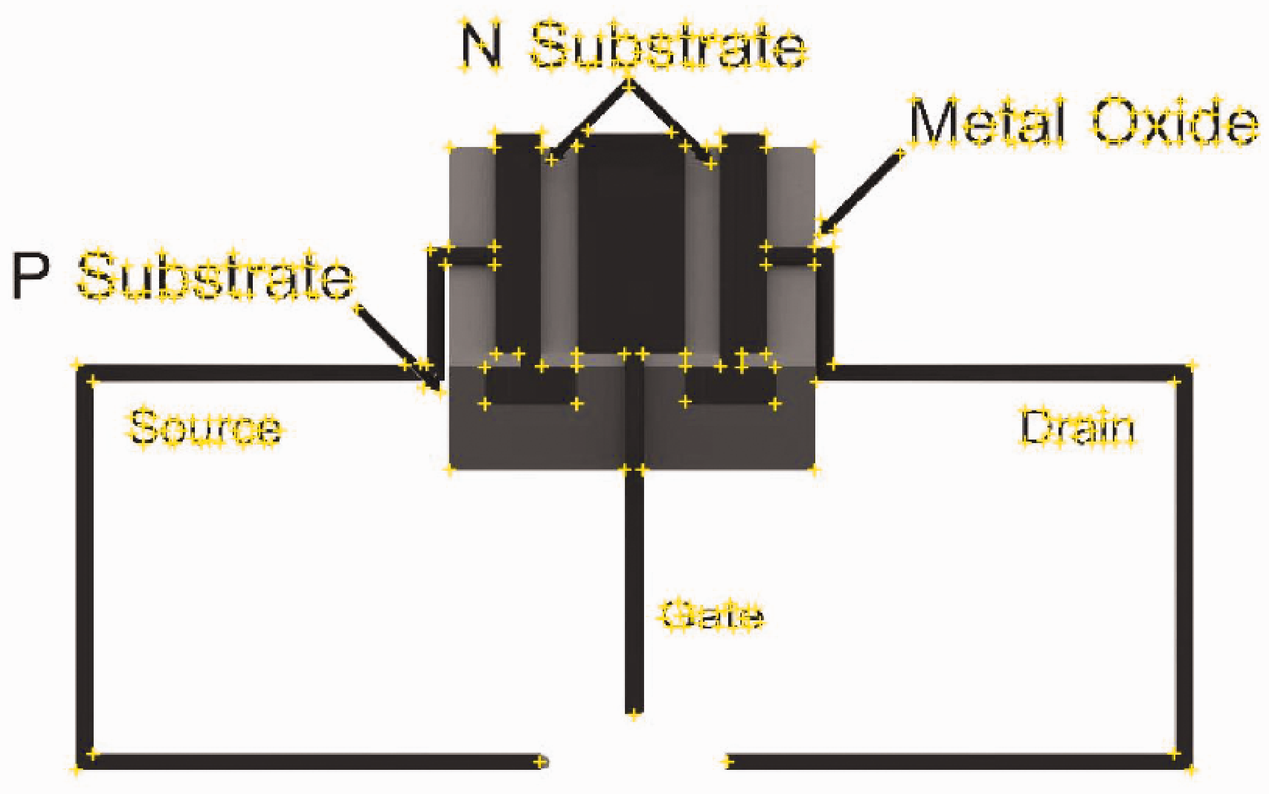
Although it was possible to model over the actual NMOS sheath during the formation of the NMOS body, and it is clear that this would be a more visually realistic representation, the modeling was performed using the internal structure representation in Figure 1 to observe the electron flow in a relatively narrow space.
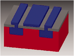
3D model of the NMOS body.
In order to insert positive and negative charges into NMOS, firstly, the body and conductors were made transparent. Then, the charges to be placed in the P type material were first placed. During the placement of the charges, more protons were modeled than electrons because the material was P type. More than 200 protons and more than 50 electrons were placed in the P type material.
Then, the charges contained in the N-type materials were placed. Electron charges in N-type materials are designed to be more numerous than protons. After the placement of the electrons and protons, the conductors connected to the ends of Source, Drain and Gate were also made transparent and the loads that would pass through the conductors and NMOS were positioned.
After the NMOS model was substantially completed, the conductors connected to the Source, Drain and Gate terminals were connected to the power supplies. A separate power supply was added to each end, and a digital display was placed in which the voltage applied to the power supplies could be read clearly. An LED was placed on the Source path to model the effect of the current flowing. Figure 2 shows the completed version of the model.
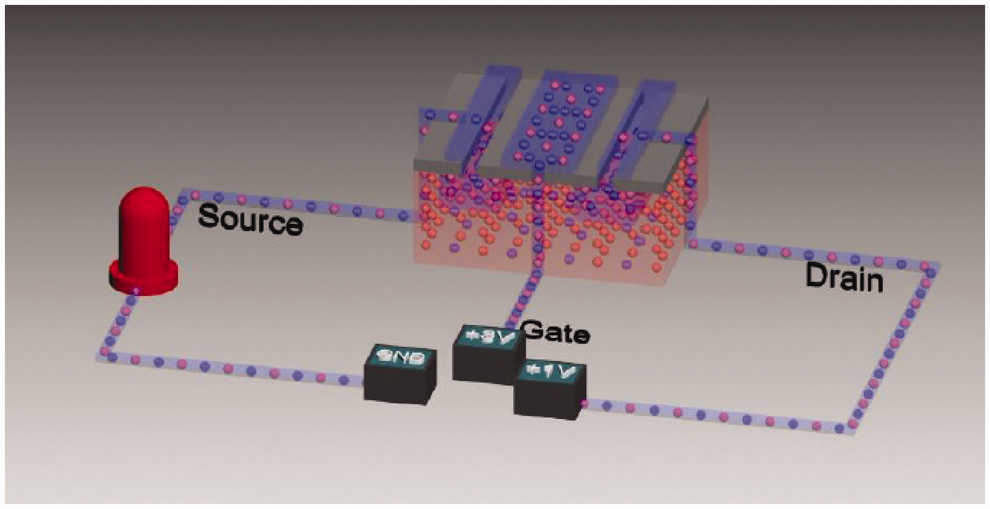
Full NMOS model.
Animations were created based on the current calculations of an NMOS transistor. NMOS has three different operation modes. These are linear mode, saturation mode, and cut-off mode. However, a fourth mode called Minimum Saturation Mode has been added to the model to clearly see the beginning of saturation. Here, saturation and cut-off modes are modeled in which NMOS will be used as on-off switch device. Firstly, for the NMOS to start transmission, the voltage difference between the Drain and Source terminals must be higher than or equal to the threshold voltage (VTN) of the NMOS. That is to say, VDS > = VTN. VTN is set here as 2 V. In the case of VDS <VGS – VTN, NMOS operates in linear mode and a thin electron bridge is formed under the gate. In this mode, a limited current begins to flow from the drain to the source. Under the condition of VDS = VGS – VTN, NMOS operates in Minimum Saturation Mode and a thicker electron bridge is formed under the Gate. Therefore, the current between Drain– Source starts to increase and the LED lights up brightly. When VDS > VGS – VTN, NMOS will be in Saturation Mode (On – closed switch) and almost all electrons in the body will be collected under the Gate as seen in Figure 3. Now, the highest possible current flows through the NMOS and the LED lights up brighter.
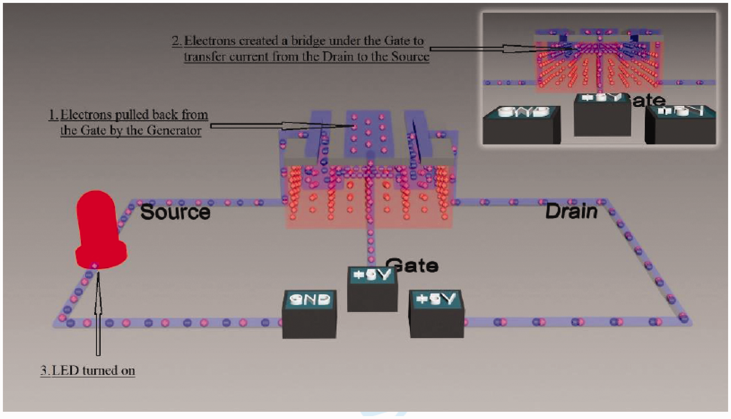
The formation of electron bridge in saturation mode.
However, if the VDS> = VTN condition is not met, NMOS operates in the cut-off mode (OFF - open switch). There will not be enough electrons under the gate to maintain the conduction and the current will be completely cut off as seen in Figure 4. Therefore, the led will turned off.
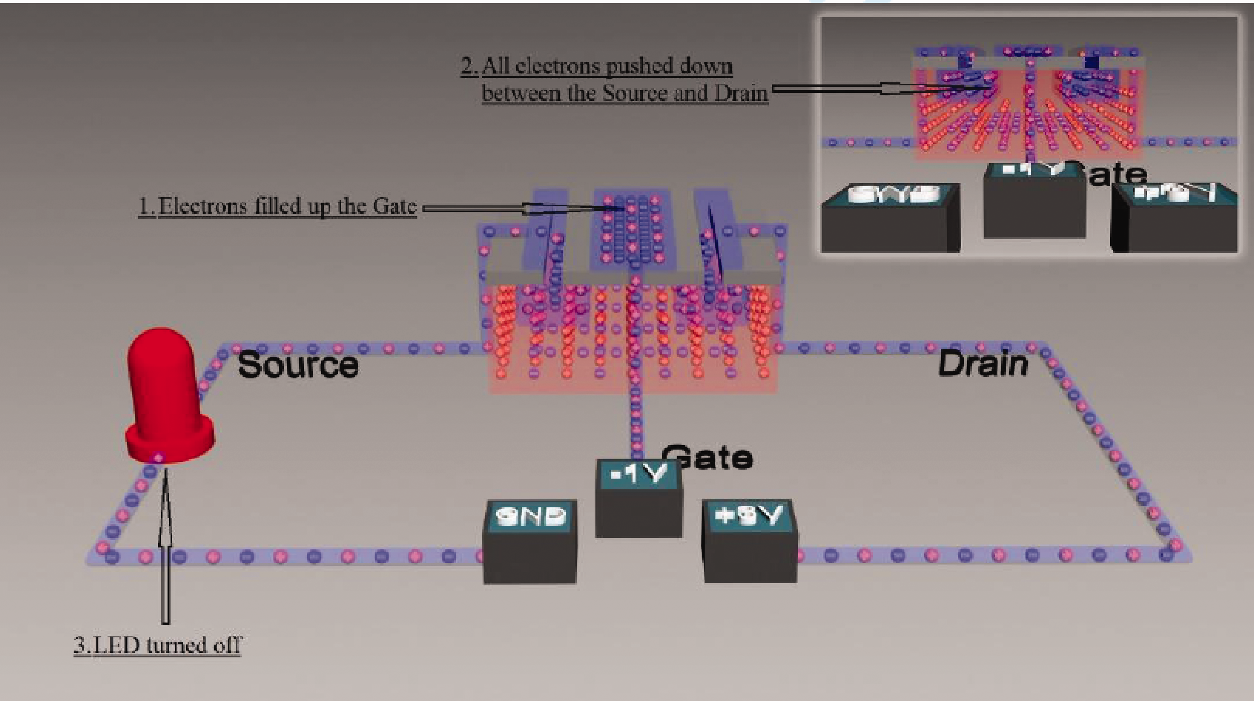
Electron deficiency under the gate in cut-off mode.
4 different animations were defined for 4 different scenarios to NMOS model whose 3D design was completed via 3Dx Max. These animations were created to simulate the work of NMOS element in Saturation, Linear and Cut off modes. This animated model was transferred to the Unity program in FBX format to be turned into AR application.
In the Unity program, Vuforia plug-in was used to produce AR applications. As shown in Figure 5, a marker has been added to Vuforia where the mobile device will position the NMOS model. The yellow marks indicate the sharp points of the shape, and these marks are compared to determine whether the shape in the camera is our pointer. In order for the 3D animation to continue showing, a certain amount of markers must be in the frame. That is, once the marker is detected, it is possible to zoom in or out of the animation. Thus, electron events can be observed from any angle or distance.
Marker defined to the Vuforia extension.
After the marker was added to the Unity program, the NMOS model in FBX format was positioned on the marker. Then, interface design was started. The interface is designed as a welcome screen with two language options (Turkish and English) and an exit button. In order to provide full interaction on the application screen, virtual buttons running animations were used. Since the virtual buttons did not work when the pointer could not be seen, the main menu and exit buttons were placed in the two lower corners of the screen. The screenshot when the software sees the pointer is shown in Figure 6. Virtual buttons appear above and below the NMOS model. The 4 virtual buttons at the bottom are designed to run animations in the Linear, Saturation, Minimum Saturation and Cut-off regions, respectively as shown in Figure 6.
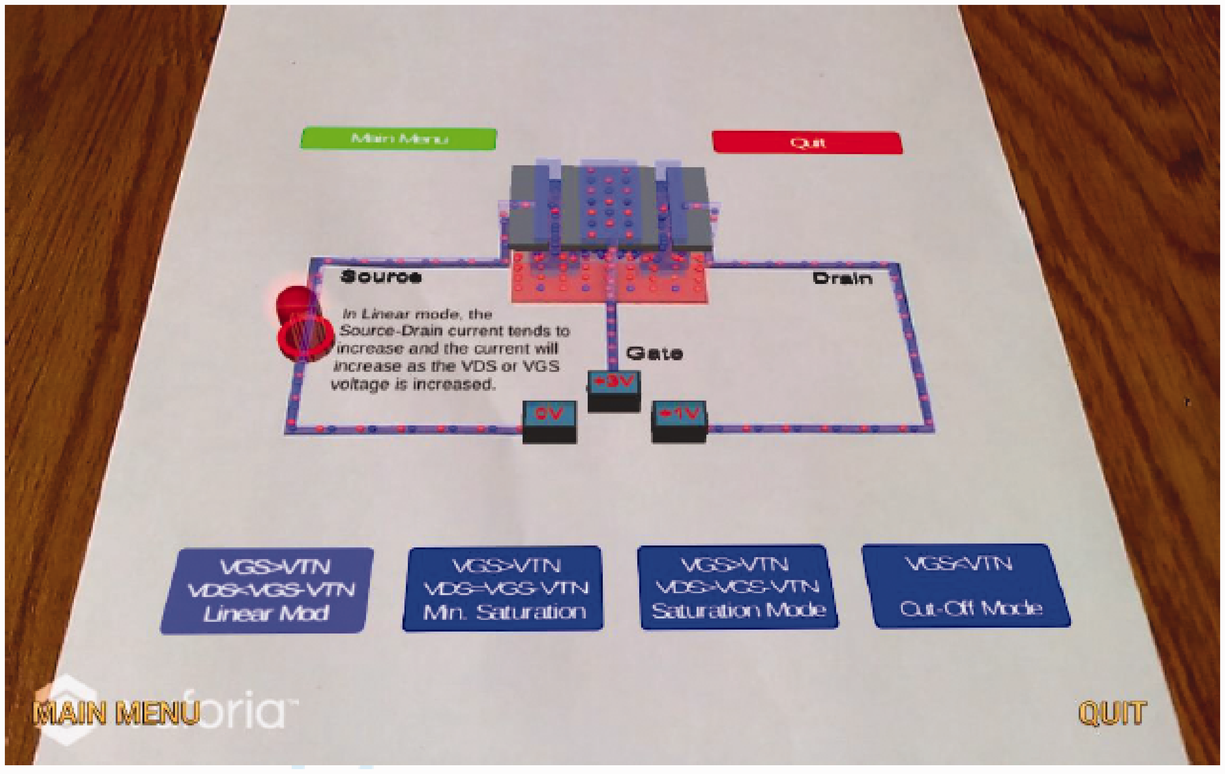
Screen shot of the software when it sees the marker.
Finally, time-varying informative texts were placed to explain the physical events that took place on NMOS when animations were played. The first version of the application was tried with some of the students and their feedback was received and improvements were made and the final version was obtained.
Test results
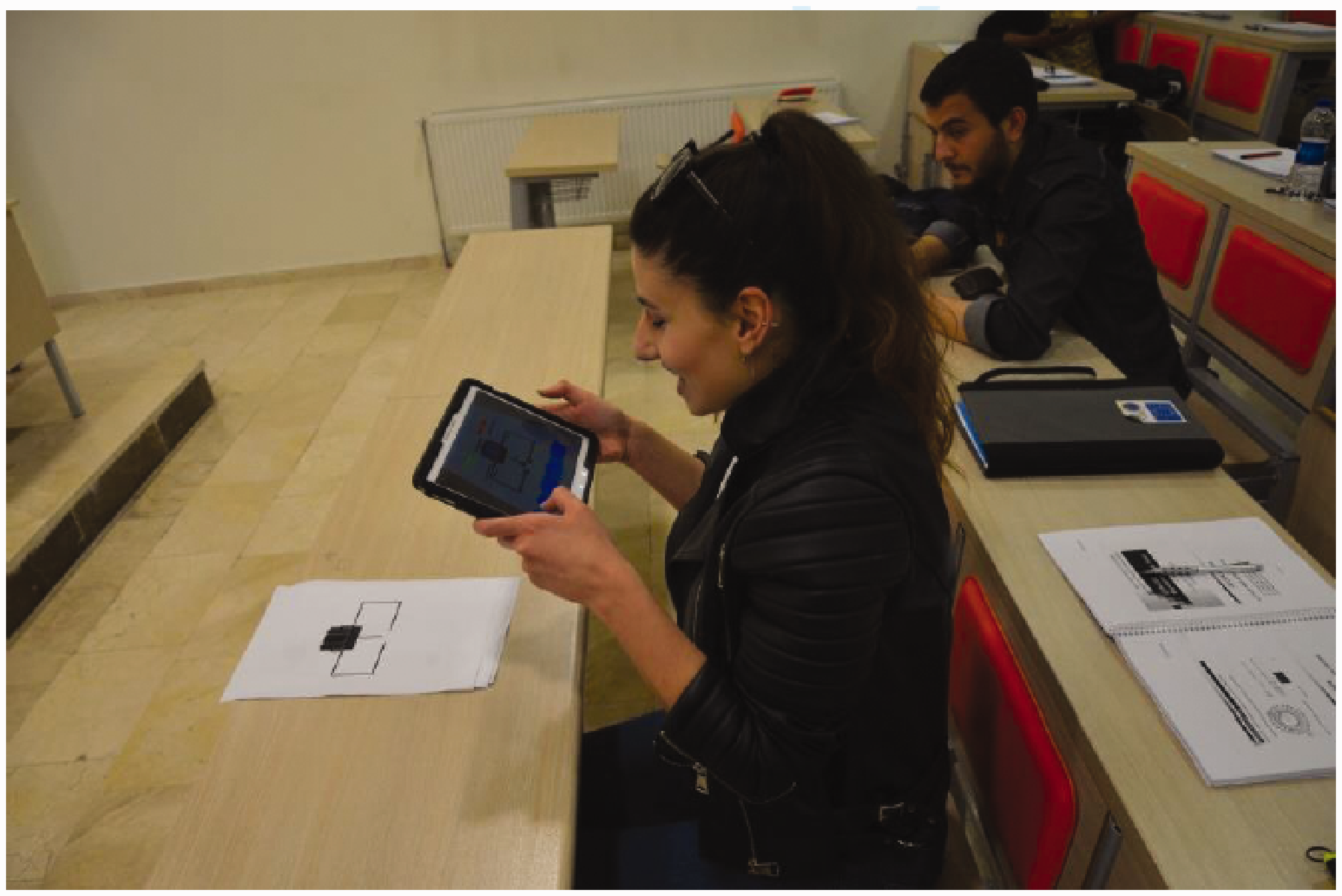
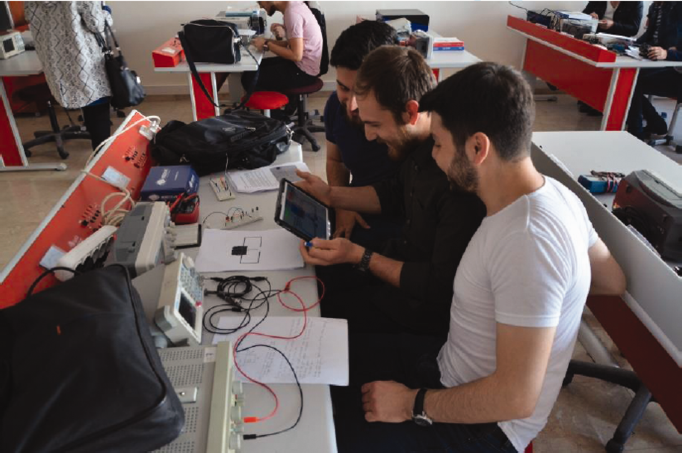
In order to determine students' opinions about AR application development in the educational setting and to compare their approach to software, the application was tested together with the 2nd and 3rd year students of Electrical and Electronics Engineering Department at Bolu Abant İzzet Baysal University. The application was carried out in one session. A total of 51 students from 2nd year students (27 out of 48 students) and 3rd year students (24 out of 56 students) voluntarily agreed to test the software. The main reason for the selection of the 2nd year student as the test group is that the students have not yet taken the theoretical principle of the NMOS element. The main reason for the selection of the third year student is that the students learned the theoretic principle of NMOS element in Analog Electronics 2 course in the previous semester.
This study aims to produce a good example of educational material that can lead the way in the field of Electrical and Electronics Engineering and inspire further studies. For this purpose, the students were asked how they felt when using the software, whether the interface was useful, and whether the animations could reflect NMOS, as shown in Figure 7. Improvements were made to the software according to the feedback.
Testing the software with the 2nd year students.
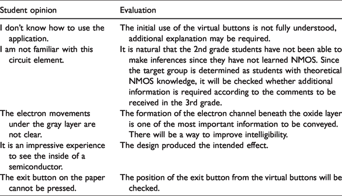
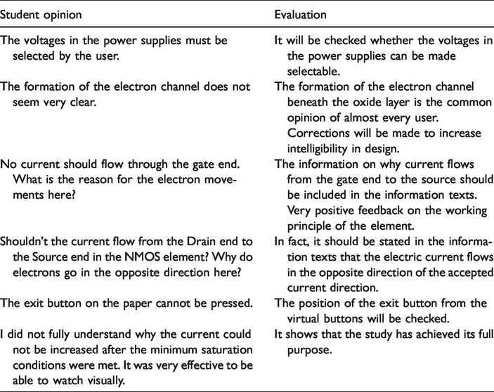
Although the total duration of the 4 animations is normally around 4 minutes, an average of 10 minutes of testing was performed with each student. Many of the students, especially those who first used AR software, were very surprised when they saw NMOS, which suddenly appeared on paper after running the software. Then, they spent some time studying NMOS by getting closer and further away. Then, by pressing the virtual buttons respectively, they watched how NMOS reacts under different operating voltages. Table 1 shows the opinions of the second year students about the AR application.
The results of tests with the 2nd year students.
The tests performed by the third year students were conducted in the laboratory environment while they were experimenting with NMOS element. This time, as it is not possible to make individual trials, as shown in Figure 8, tests were conducted with 7 experimental groups ranging from 1 to 4 people on the basis of experimental groups. Table 2 demonstrates the opinions of the 3rd year students about the AR application.
Testing the software with the 3rd grade students.
The results of tests with the 3rd year students.
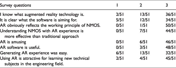
A survey consisting of 8 questions was applied to determine the effect of AR technology on students. The purpose of these survey questions is to find out whether students help AR technology to understand the working principle of NMOS, to have information whether students are interested in using AR technologies and to determine if Electrical and Electronics Engineering students like AR experience. The survey uses a 3-point scale: 1 – Disagree, 2 – Neither Agree nor Disagree and 3 – Agree.
Table 3 shows the survey questions and answers. When the answers to the survey were evaluated, it was observed that the students noticed the advantage of using AR technology as an educational material in the field of electrical and electronic engineering. In addition, it has been observed that especially 3D representation with AR technology makes learning more enjoyable and more permanent. As a result, augmented reality is technology that can have a positive impact on engineering field.
The results of the answers to the survey questions.
Conclusion and suggestions
Considering the fact that everyone has at least one mobile phone in the pocket in today's technology age, developing Augmented Reality applications should be among the most important investments that can be made in the field of education and training techniques. In this study, in order to develop an exemplary AR application, the working principle of the NMOS element, which is one of the issues that are difficult to understand between the courses of Electrical and Electronics Engineering, is modeled. After the software was developed, it was observed in the experiments conducted with the students that the power of AR technology to embody abstract concepts made a significant contribution to the perception of abstract concepts and significantly increased the motivation of the students to the subject. The results of test conducted in previous scientific studies in this area also confirm this observation.
It was observed that although the developed application met the objectives largely, the students who tested the software did not meet all of their demands. It is thought that the application can be developed in such a way that the electron movements can react according to the voltage values determined by the user rather than being designed as separate, standard scenarios.
Based on the fact that AR technology and tools make learning more enjoyable and permanent and can have a positive effect on technical subjects, the development of AR training material especially in the field of Electrical and Electronics Engineering can make a significant contribution to education-teaching in the courses such as Electromagnetic Field Theory, Analogue Electronics, Digital Electronics, Signal Processing, and Circuit Analysis.
Footnotes
Declaration of conflicting interests
The author(s) declared no potential conflicts of interest with respect to the research, authorship, and/or publication of this article.
Funding
The author(s) received no financial support for the research, authorship, and/or publication of this article.