
Abstract
An automated textile circuit generation method was developed using machine vision and embroidery technique. For this, an image acquisition device was designed to capture the physical layout image of electronic devices on the fabric. A series of image analysis algorithms were developed to calibrate the image and recognize the type, location, and orientation of each device from the image. Dedicated computer-aided design software was developed that can design a circuit and modify it according to the actual device layout on the fabric. It can also convert the circuit elements such as conductive path and insulation layer into data for a computerized embroidery machine. An example circuit consisting of seven electronic devices was designed and repeatedly produced to verify the developed method. The method has shown promising results.
Conductive embroidery was first tried in research undertaken by MIT Media Lab, and has become one of the most appealing techniques to realize smart textiles. Compared with other traditional textile manufacturing techniques such as weaving and knitting, embroidery can arrange threads in any direction, which is a great advantage when making textile circuits. Using embroidery, the essential elements of a circuit, such as electrodes, the conductive path, and insulation can be seamlessly integrated into the clothing. 1
Conductive embroidery has been widely studied over the last few decades. One of the most actively studied subjects in this field is the textile antenna, which has been used successfully in RFID (radio frequency identification) 2 and WBAN (Wireless Body Area Network). 3 Tsolis et al. 4 compared the performance of textile antennas. Linz et al. 5 introduced embroidery as a method of connecting electronics to textiles. In recent studies, conductive embroidery has been utilized for implementing flexible, wearable electronics such as soft actuators6,7 and sensors. 8 The washability of embroidered circuits has also been investigated. 9
For the embroidery technique to be utilized for the manufacturing of textile circuits in practice, the process of combining elements of different physical properties needs to be optimized. 10 However, general embroidery design software requires significant person hours to generate a valid circuit, since it is developed to fulfill mainly decorative purposes. Eichinger et al. 11 automated the circuit design process by converting the output of Eagle, a printed circuit board (PCB) design software, into embroidery data. Hamdan et al. 12 developed a new method of creating embroidery data by analyzing hand-drawn circuit images. Even though these efforts have reduced some of the manual work required, the placement and joining processes of electronic devices remains laborious. This is mainly because the accurate placement of devices is very important to prevent collisions between needles and devices when attaching the devices to the fabric using embroidery technique. Linz et al. 5 incorporated extra stitches to indicate where the electronic devices should be placed. Dias 10 proposed attaching a sensor to the target device to detect its location. A German embroidery machine manufacturer, ZSK Stickmaschinen (Krefeld, Germany), suggested using a robotic arm to place the electronic device at a certain location. 13 However, from an industrial point of view, a more efficient method is needed to realize the secure and reliable joining of fabric and various electronic devices.
In this study, an automated process for a textile circuit generation method was developed using machine vision and dedicated computer-aided design (CAD) software. An image acquisition device was designed to capture the layout of electronic devices on the fabric. An image analysis algorithm was developed to recognize the type, location, and orientation of each device. CAD software was developed to enable its users to easily make a circuit using the device database and interactive graphical user interface. Finally, the conductive path information in the circuit was converted into data for a computerized embroidery machine. Once designed, the circuit can be automatically modified according to the actual physical layout of the device. To verify the validity of this method, an example circuit consisting of 7 electronic devices and 12 conductive paths was designed and repeatedly produced. The method has shown promising results.
Machine vision process
Overall circuit generation process
The textile circuit generation process developed in this study consists of three parts including machine vision, CAD software, and conductive embroidery. The workflow is as shown in Figure 1.
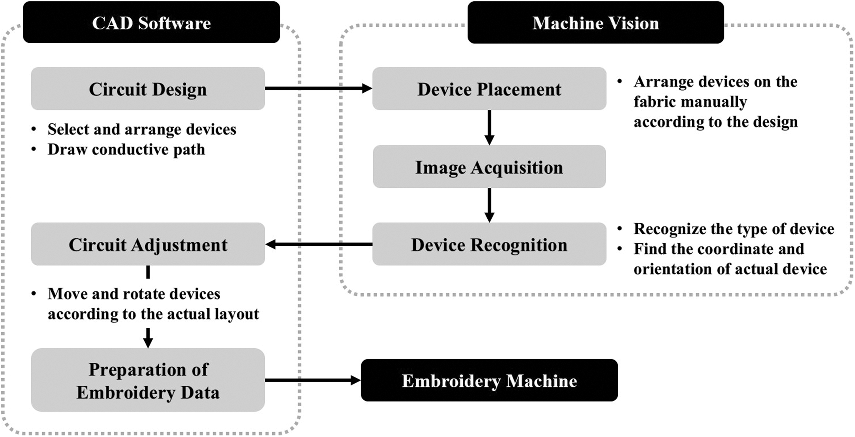
Overall process.
First, a circuit was designed using CAD software and the electronic devices in the circuit was placed on the fabric according to the design in Figure 2. The green line in Figure 2 indicates the outline of the device; the blue line shows the conductive path for connecting the devices. The image acquisition device then captured the layouts of the electronic devices as shown in Figure 2(a). The type, location, and orientation of each device were recognized through image analysis. The center of the frame was determined by recognizing the eight red dots marked on the frame as shown in Figure 2. The intersecting red lines were drawn to show the center of the image. Since the frame was fixed at the same position with respect to the embroidery machine, it was possible to convert image coordinates to real coordinates using this information. The original circuit was then modified according to the actual device layout as shown in Figure 2(b). Finally, the conductive path information for stitching and joining was converted into data for a computerized embroidery machine for actual production.
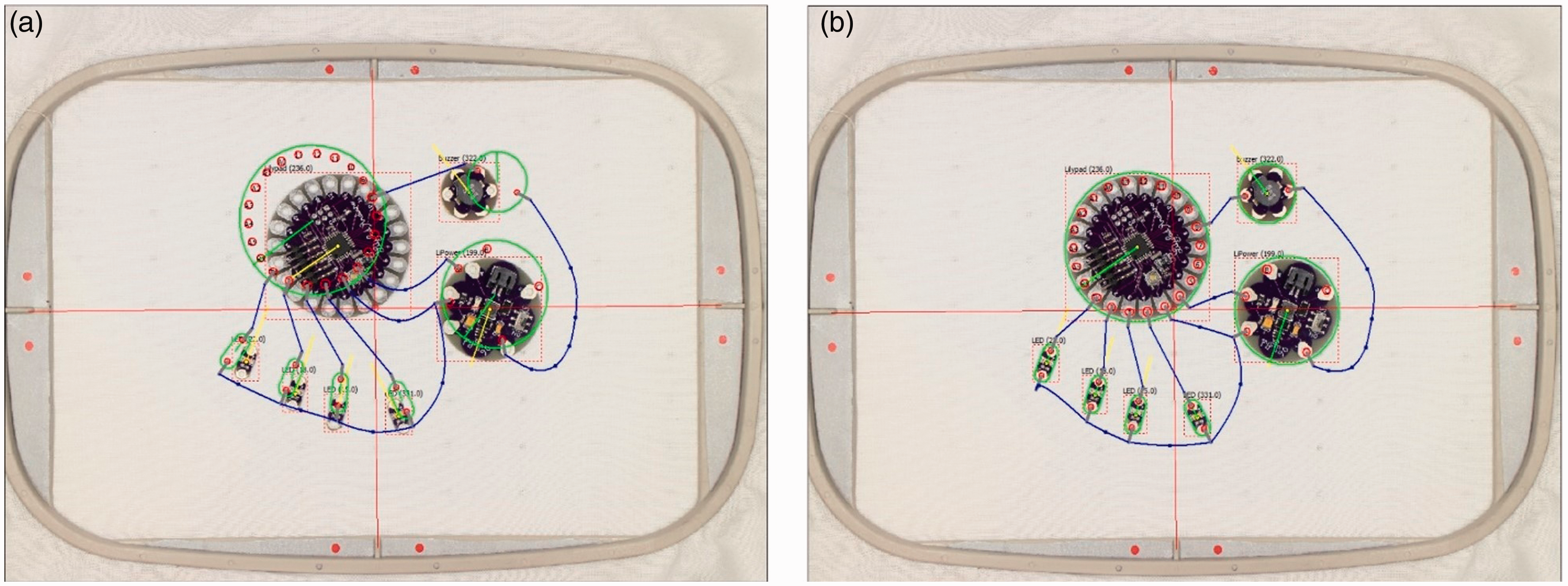
Example of device alignment (a) before alignment and (b) after alignment.
Image acquisition device
Acquisition of a stable and clear image is one of the most important steps in machine vision. In this study, an image acquisition device was designed, as shown Figure 3. It consisted of an aluminum profile frame, a high-resolution digital camera, two LED surface lamps, and a calibration plate. Canon's EOS-M digital camera with an EF-M lens of focal length 52 mm was used and the size of the captured image was 2592 × 1738 pixels. The memory required for a single image was 13.51 MB.
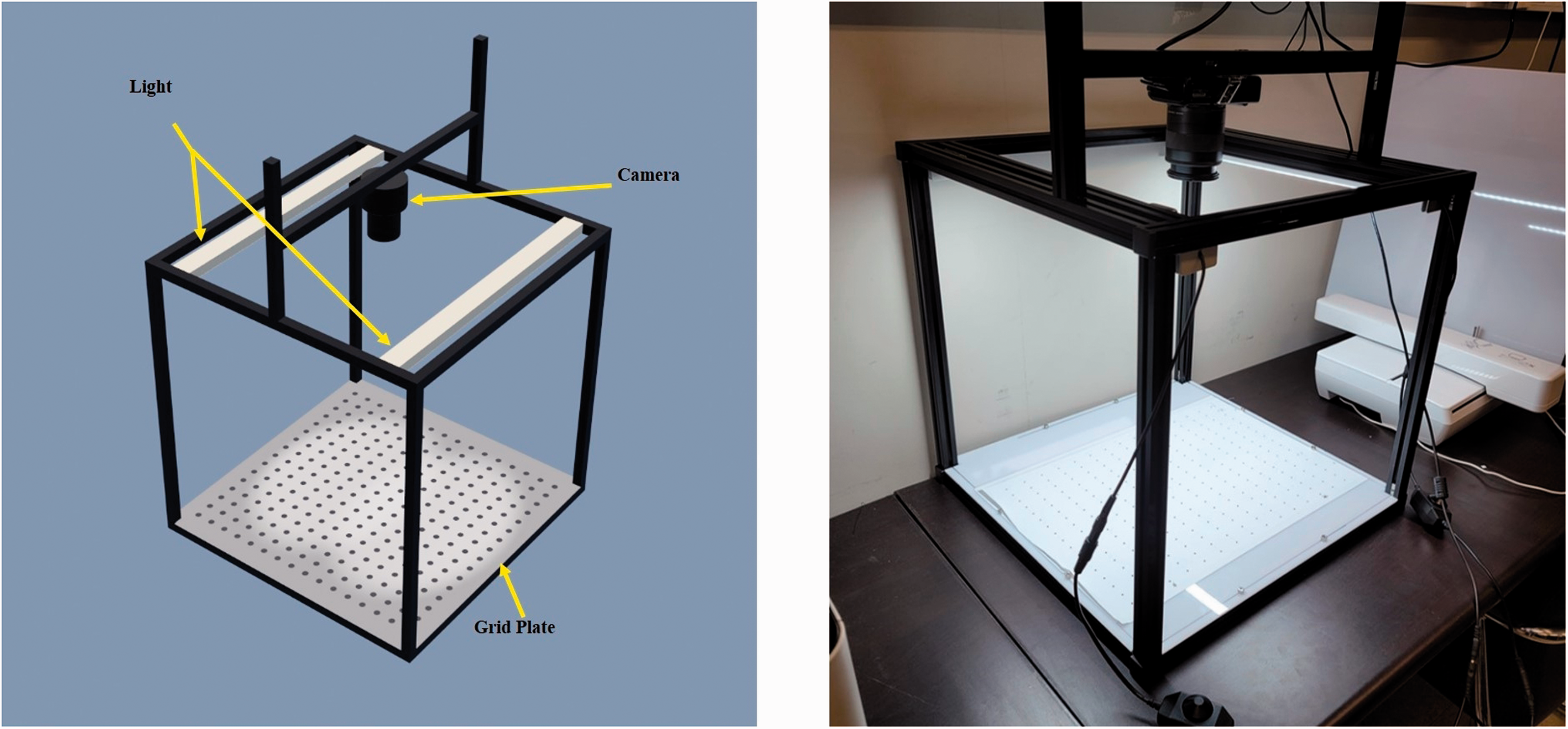
Overview of image acquisition device.
Camera calibration
Due to various factors such as a lens aberration or misalignment of the camera assembly, there can be a considerable amount of distortion in the images acquired by a camera. Therefore, a calibration process for correcting them is essential to realize accurate machine vision. In this study, the calibration of the image was performed by constructing a rectangular grid using a calibration plate that incorporated a dot grid as shown in Figure 4. Using this grid, the relationship between the image coordinates and the real-world coordinates could be established. 14 First, the image of the dot grid was binarized into a black and white image through thresholding. Then, labeling 15 was applied to that image to find the grid points. Finally, a rectangular grid system was formed by connecting those points as shown in Figure 4(b). The image coordinate of each pixel inside the grid could then be converted into real-world coordinates using isoparametric mapping. 16 In order to achieve the ideal speed and accuracy for image analysis, the resolution of the image was set to 5 pixels per millimeter.
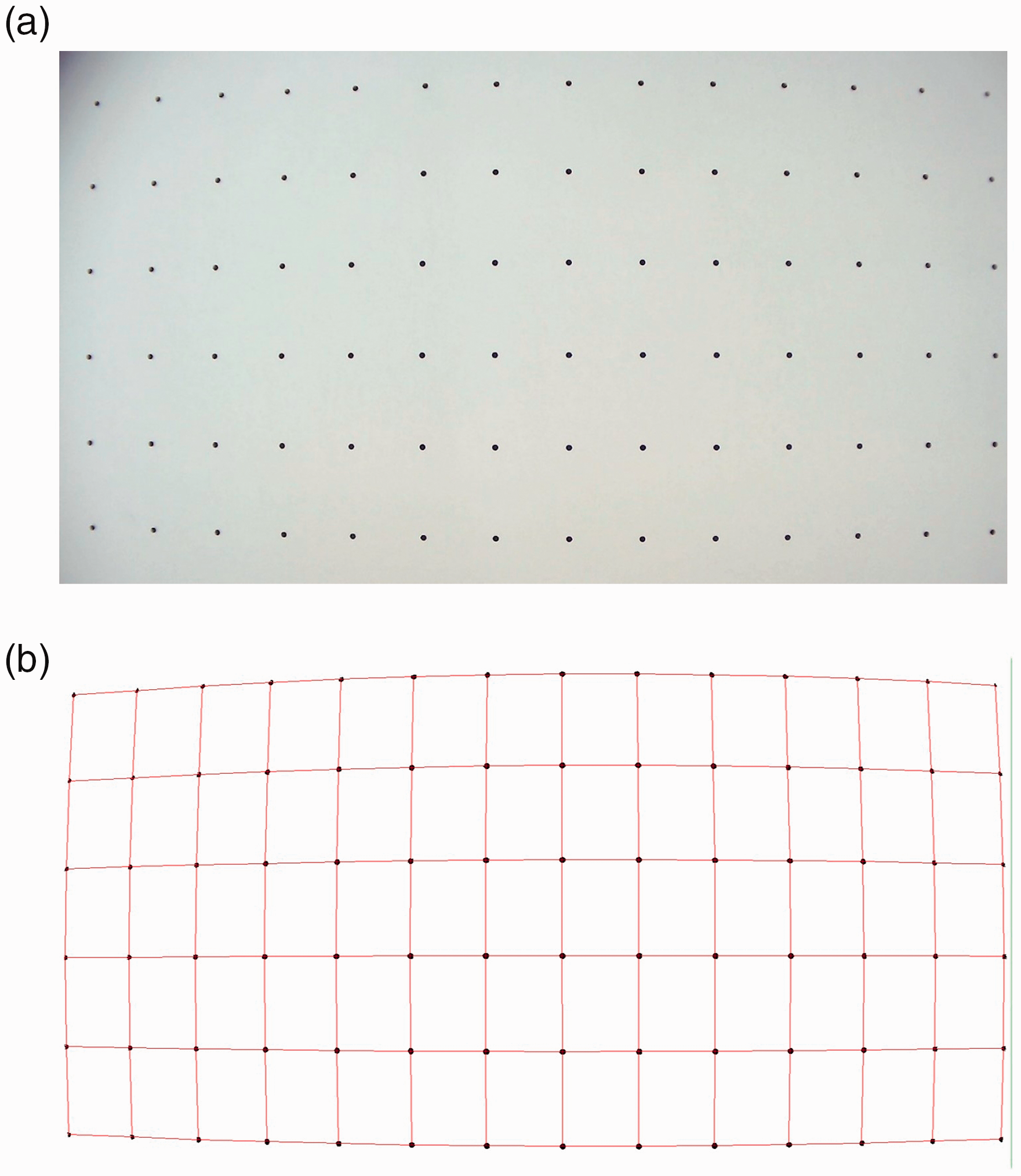
Schematic diagram of camera calibration: (a) calibration plate image and (b) reconstructed rectangular grid.
Device database and device recognition algorithm
In this study, a device database was used to facilitate the circuit design as well as the recognition of devices. The database contained the visual characteristics of each device, required for recognizing their location and orientation as well as the positions of the electrodes. Figure 5 presents an overview of the device database manager.
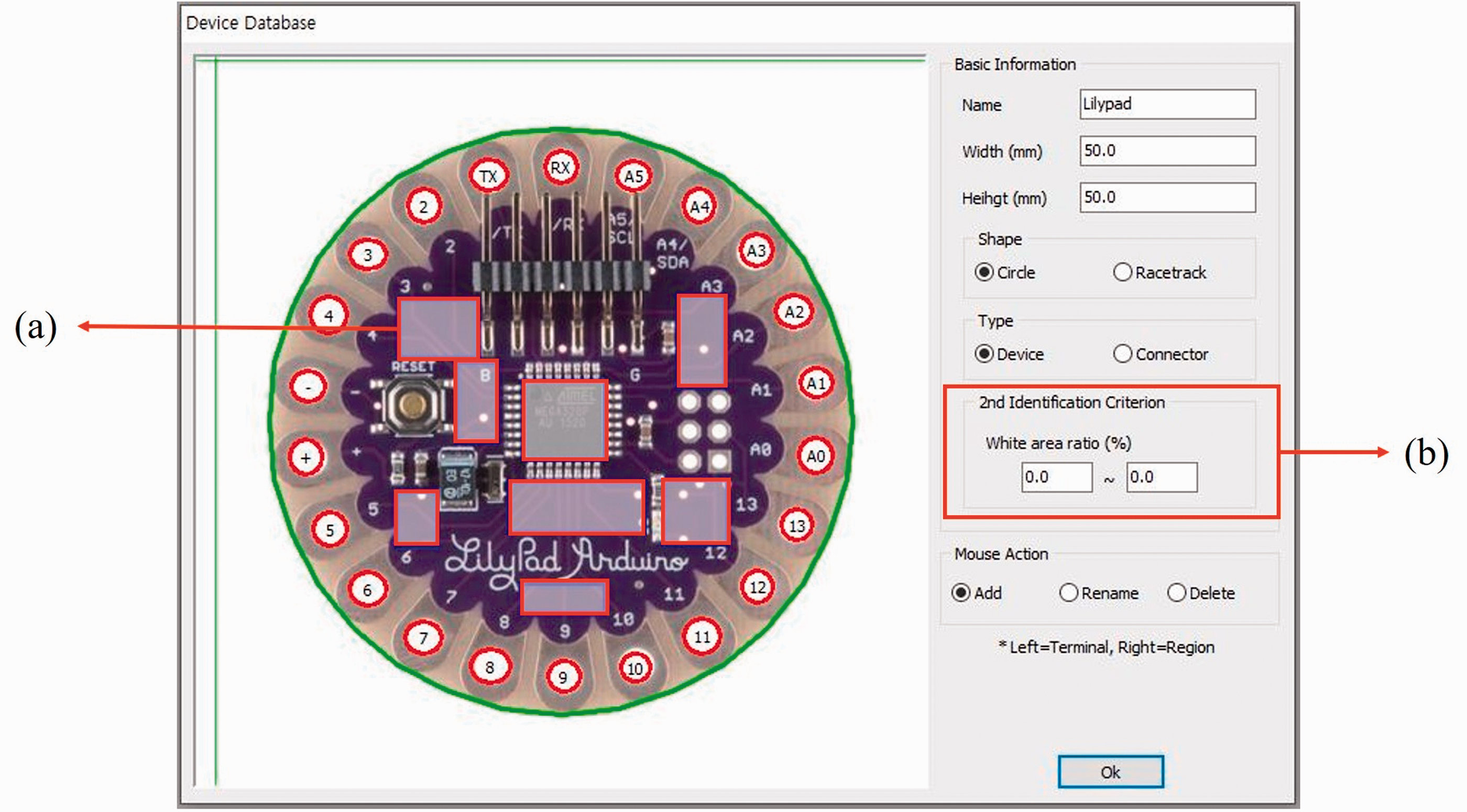
Overview of device database manager: (a) definition of even color zone and (b) definition of white pixel ratio.
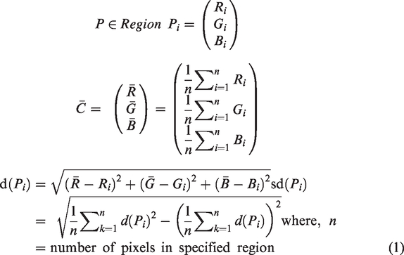
The database manages two types of device information: functional and visual features. The type, location, and size of each electrode on a device are the functional features, while size and shape are the basic visual features used for device recognition. In this study, some additional visual features were proposed to recognize the devices, which are different in function but the same size and shape. The white pixel ratio refers to the number of white pixels to the total number of pixels in a specific region of a binary image. The user can set the upper and lower limits of the white pixel ratio to each device, as shown in Figure 5(b); the ratio is a further criterion that is used when it is impossible to classify a device by its shape and size alone. The white pixel ratio tends to have different values according to the function of a device (see Figure 6). The even color zone is an area of relatively even color distribution on the surface of the device, which is used to determine the orientation of the device. The user can exercise their judgment to define as many zones as needed where there is little color fluctuation on the surface of a device, as shown in Figure 5(a).
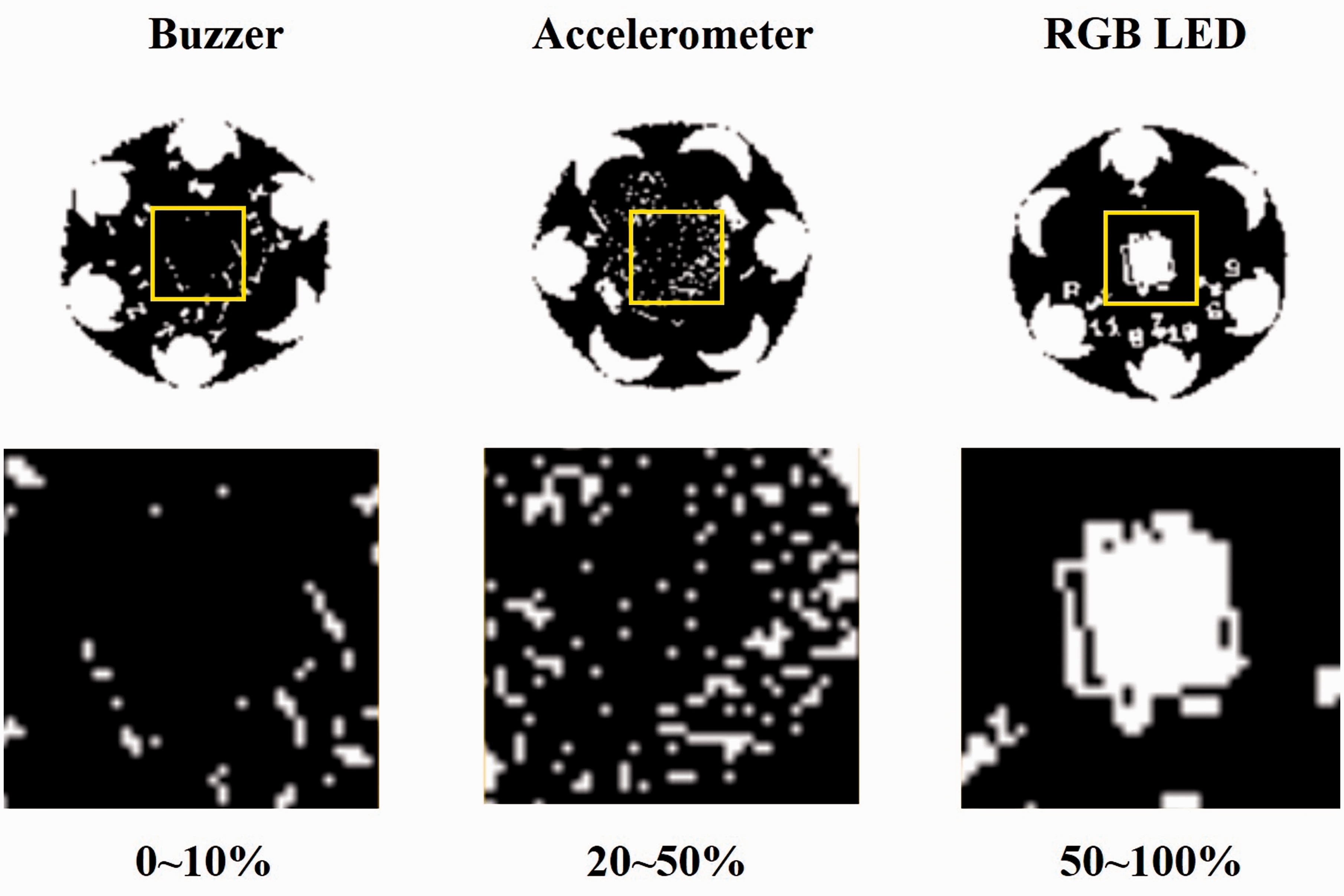
Example of white pixel ratio.
The image processing needed for device classification is as shown in Figure 7. Were the labeling performed directly on the binary image just after thresholding, it would be difficult to recognize a device due to the noise in its image. Therefore, the dilation technique was used to remove the noise by changing the white pixels that touch the black pixels into black pixels. 17 Most devices can be classified by comparing the occupied area of the black pixels found through labeling with the information in the device database. As mentioned earlier, the white pixel ratio is considered to further classify devices of a different type but the same size. When the type of a device has been determined, the center of the occupied area becomes the location of that device.
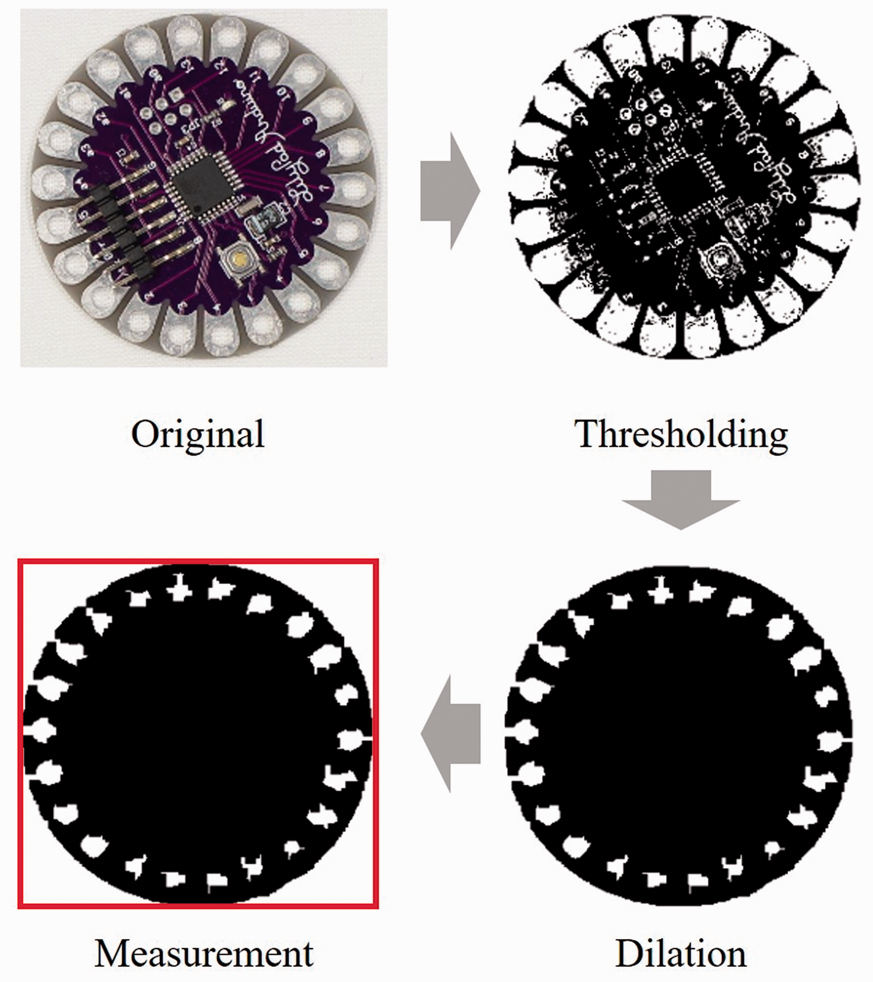
Image processing for device recognition.
In this study, an algorithm was developed to determine the orientation of a device based on the template matching technique. Template matching is the method of finding the target object similar to a reference image using a pixel-based comparison operation. 18 This technique can obtain the coordinates, orientation, and size of an object with very high precision even with a small data sample. 19 First, a template was created as a mask (Figure 8(b)) based on the predefined even color zones as shown in Figure 8(a). Then, the standard deviation of the color in the even color zones was calculated while rotating the template mask. Finally, the angle at which the deviation of the color was at its minimum was determined as the orientation of the device.
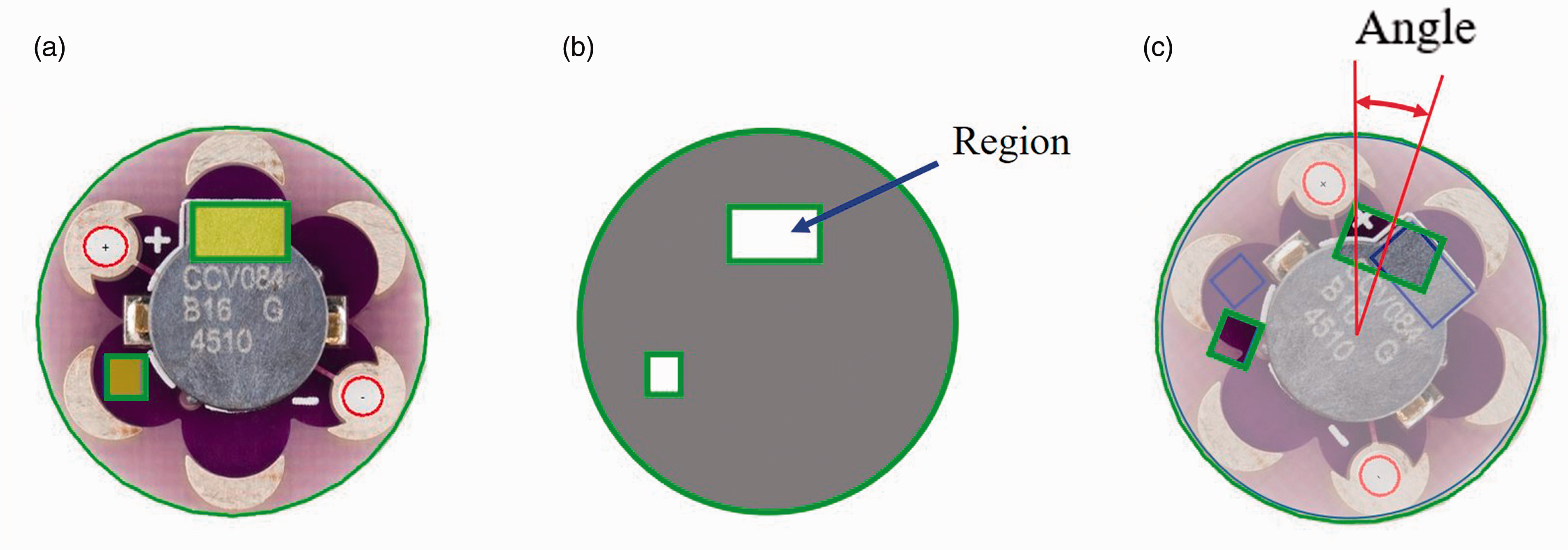
Schematic diagram of template matching algorithm: (a) even color zone, (b) template, and (c) masking operation.
Figure 9 shows the flow of this algorithm.
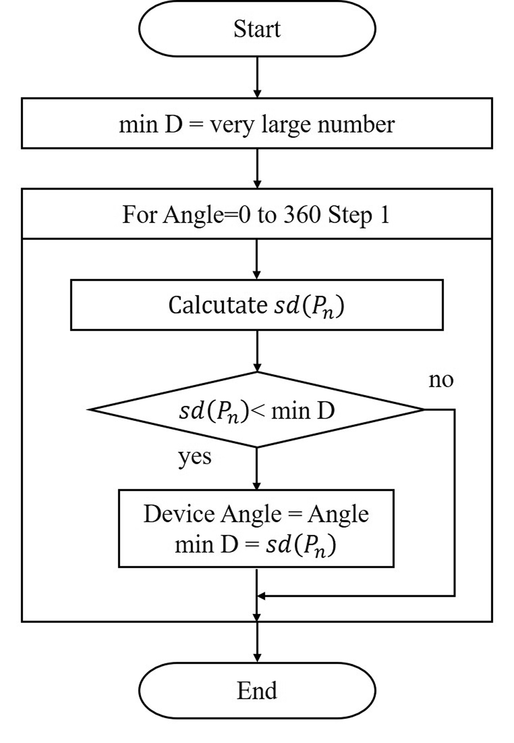
Flow chart of device orientation determination algorithm.
The deviation of color in a region,
The original circuit designed by the CAD software that was developed in this study can be modified automatically according to the actual physical location and orientation of each device recognized through the algorithm explained above, which is expected to reduce the amount of manual work required for the accurate placement of electronic devices.
Circuit design software
Circuit design process
The overall textile circuit design process was as follows. First, each electronic device was placed at the desired location and the paths connecting the terminals of the devices were defined. Next, the circuit was modified according to the actual physical position and orientation of each device recognized through machine vision. Finally, the conductive path information was converted into the data for a computerized embroidery machine, taking into account stitch type and stitch length. In this study, a dedicated CAD software was developed to allow users to easily design the circuits using C++ Builder 10.2 (Embarcadero, USA)
User interface
The user can place various devices within the valid work area of the embroidery machine using an intuitive drag-and-drop interface. The conductive path between two terminals can also be defined easily as follows. When the user chooses two terminals that need to be connected, the path stitch and the joining stitch are automatically generated as shown in Figure 10. The stitch information is then converted into DST (Data Stitch Tajima) data format, one of the most widely used information exchange data formats for computerized embroidery machines.
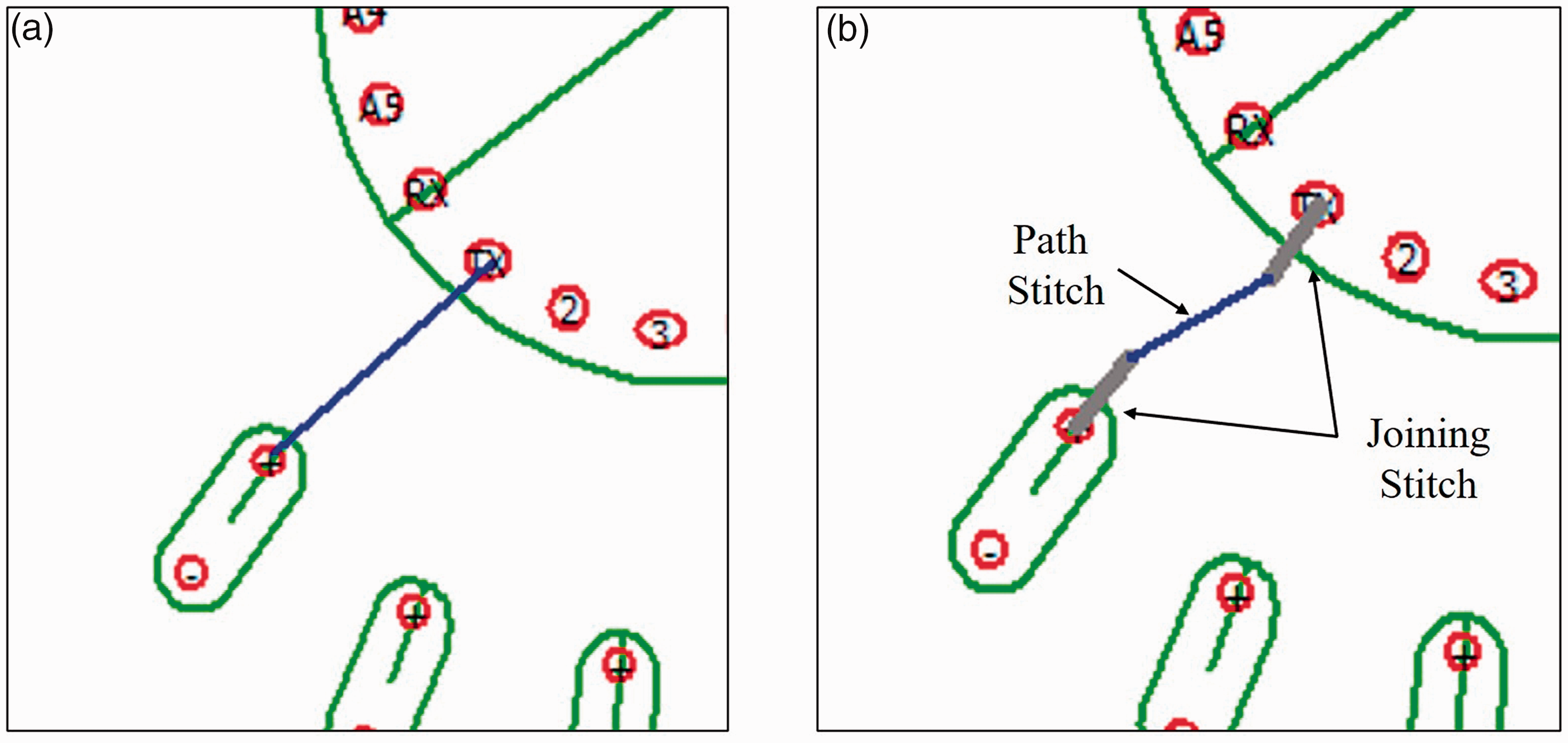
Diagram of path generation: (a) initial definition of path between two terminals and (b) generation of path and joining stitches.
Embroidery circuit generation
Three types of stitches were used for the generation of textile circuits as shown in Figure 11. The path stitch was a trace through which electric current flowed and it was fabricated using a running stitch (Figure 11(a)). The joining stitch was used to attach the electronic devices to the fabric (Figure 11(b)). It consists of multiple running stitches over a terminal, which were automatically made in a straight line connecting the center of the device and the terminal. One of the technical challenges in a textile circuit is the possibility of a short circuit and damage caused by rubbing or washing. To solve this, an insulation stitch was made using a satin stitch with a non-conductive thread over the conductive path as shown in Figure 11(c). 9 Insulation stitches were automatically created along the path stitch. The width and pitch of each stitch can be defined by the user.
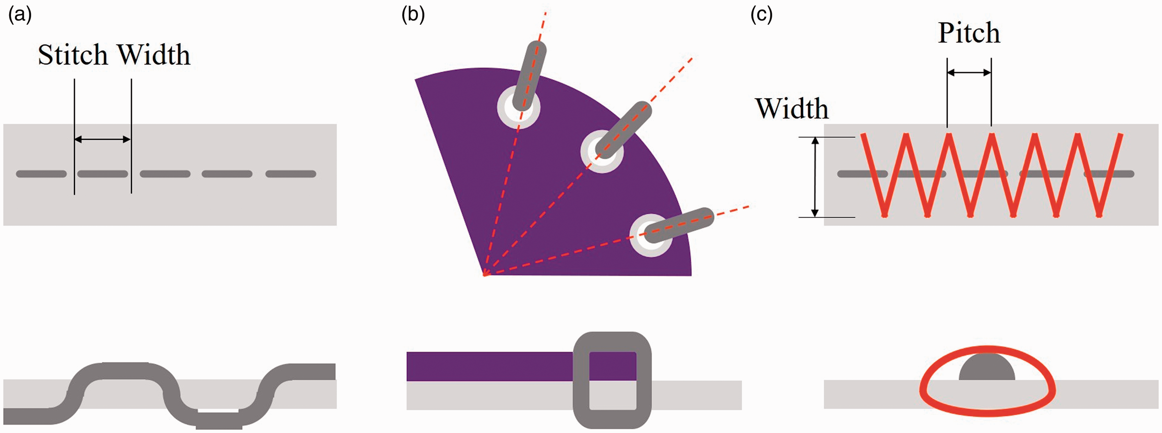
Diagram of types of stitches used for textile circuit formation: (a) path stitch, (b) joining stitch, and (c) insulation stitch.
Experimental results
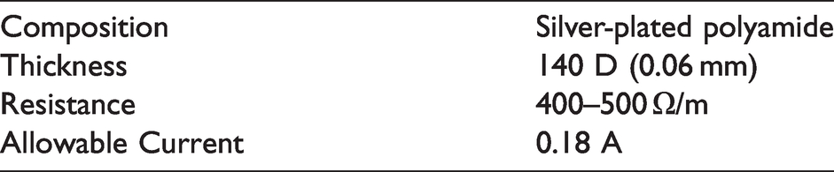
An NV 2600 computerized embroidery machine with a maximum speed of 350 spm (stitches per minute) and a work area of 130 × 180 mm was used for the fabrication of the circuits (Brother Industries Ltd., Japan). A hundred percent polyester 120 D sewing thread was used for the bobbin thread and insulation stitch. The conductive thread was used for path and joining stitches. Among the various conductive threads, a silver-plated polyamide yarn was chosen because it was light, flexible, and mechanically stable enough for machine embroidery. 20 The properties of the conductive thread used in this study are as shown in Table 1.
Properties of conductive thread
A 20 count 100% cotton, plain weave, white fabric was used as the base fabric of the circuit. The LilyPad Arduino device series, the most widely used in the form of a sewable PCB, was chosen as the device for the textile circuit.
An example circuit was designed for the verification of the method developed in this study. It consisted of seven electronic devices including a LilyPad Arduino controller, a LiPower, four LilyPad LEDs, and buzzers. Twelve conductive paths were defined to connect the devices as shown in Figure 12.
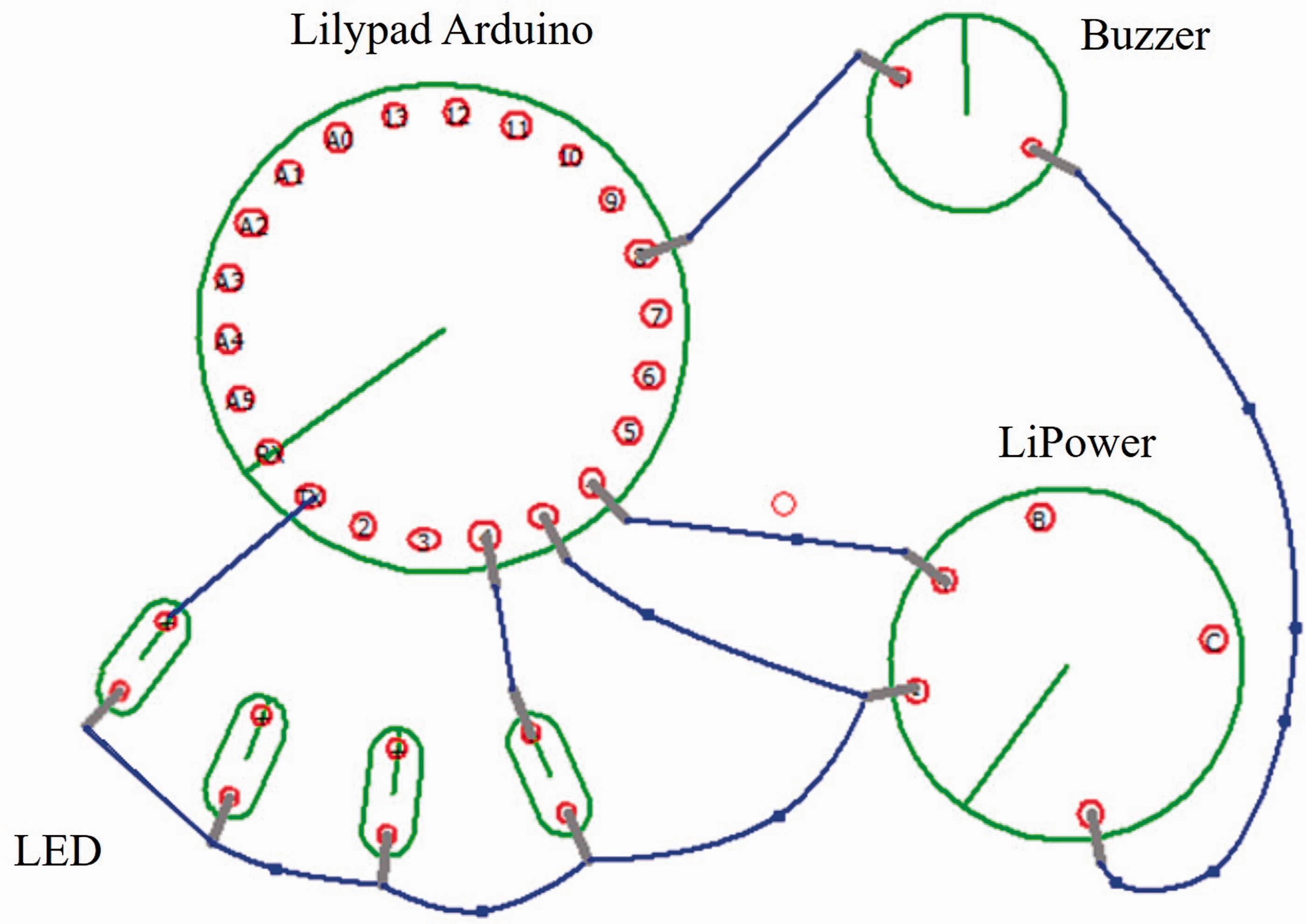
Test circuit design.
Finally, three physical circuits were produced by arranging the devices (Figure 13). The original circuit was modified according to the actual device layout. The conductive paths were made automatically by embroidery technique and all the resulting circuits operated properly.

Examples of test circuits.
Conclusion
In this study, an automated production method of a textile circuit was developed using machine vision and embroidery technique. An image acquisition device was designed to capture an image of the layout of the electronic devices. An image analysis algorithm was developed to recognize the type, location, and orientation of each device. A dedicated CAD software was developed to enable users to design circuits easily by placing and connecting the electronic devices using an intuitive graphical user interface. The software has the capacity to automatically modify the original circuit according to the actual physical layout of devices on the fabric. Finally, the circuit information was converted into data for a computerized embroidery machine. To verify the validity of the developed methodology, a test circuit with seven devices was designed and produced three times. The method has shown promising results.
The accurate placement of electronic devices is one of the biggest challenges in textile circuit generation using embroidery technique. The methodology proposed in this study is expected to facilitate the design and production of textile circuits without expensive additional equipment or expertise in embroidery technique.
Footnotes
Declaration of conflicting interests
The author(s) declared no potential conflicts of interest with respect to the research, authorship, and/or publication of this article.
Funding
The author(s) disclosed receipt of the following financial support for the research, authorship, and/or publication of this article: This work was supported by the National Research Foundation of Korea (NRF) Grant funded by the Korean Government (MSIP) (NRF-2016R1A5A1938472).