
Abstract
Long range optical rulers measuring distance greater than 10 nm have important applications in monitoring biological processes, nanolithography, and nanometrology. In this work, we show that lateral displacement over 120 nm can be determined by measuring two reflection peaks of the proposed nanostructure. The optical anapole in the nanostructure is excited, resulting from interactions of plasmonic resonance modes of nanoholes perforated in metal films and an array of nanoblocks. Results show that a 120 nm relative displacement between the nanoblocks and nanoholes induces a negative correlated 90% variation of reflection spectrum which can be used for self-referenced measurement. The proposed design could find applications in nanometrology, biosensing, and nanofabrication.
Introduction
The so-called “plasmon ruler” using the near-exponential distance decay and scaling behavior of interparticle plasmon coupling has been widely studied and applied in biosensors, material technology, and photonic devices (Butet and Martin, 2014; Dolinnyi, 2015; Jain et al., 2007). The distance dependence of plasmon resonance in nanostructures and nanoparticles offers plasmon ruler a unique advantage that a wide range of distance from angstrom to hundreds of nanometers could be measured (Hill et al., 2012; Li et al., 2015; Ray et al., 2014). It has been shown that three-dimensional configurations of a plasmonic nanostructure supporting Fano resonance can be determined by measuring the second-harmonic scattering (Butet and Martin, 2014). Recently, an optical ruler using metasurface with sub-nanometer displacement resolution has been proposed and demonstrated (Yuan and Zheludev, 2019).
Plasmonic sensors are based on multimode interferences and multipolar interplay in metallic nanostructures which lead to complex electromagnetic response with peaks in the far-field extinction spectra. Particularly, destructive interference of the electric and toroidal dipole moments produces a low-radiating optical anapole mode that has found applications in nanoantennas, active photonics, and metamaterial (Baryshnikova et al., 2019). It has been experimentally demonstrated that combining dumbbell aperture and vertical split-ring resonator can produce anapole mode in the infrared range (Wu et al., 2018). The optical anapole mode requires selective excitation of toroidal multipoles that needs accurate engineering of the nanostructure to match the near-field modes interaction (Yang and Bozhevolnyi, 2019).
In this work, we show that self-referenced nanometric displacement sensing can be achieved by a planar nanostructure assisted by optical anapole mode, as shown in Figure 1. The proposed structure consists of an array of intersected double nanoholes (DNHs) perforated on a gold nanofilm, placed on a simple periodic nanoblocks, separated by a dielectric layer. The relative nanometric displacement between the DNHs and the nanoblocks could be measured by detecting the reflection or transmission spectra (Figure 1(a)). The optical properties of the proposed device are studied by the finite difference time domain (FDTD) method. Results show that there are two distinctive peaks exhibited in the reflection/transmission spectra which are correlated with the displacement. This correlation between the two resonance peaks of the reflection/transmission spectra enables self-referenced detection of nanometric displacement.
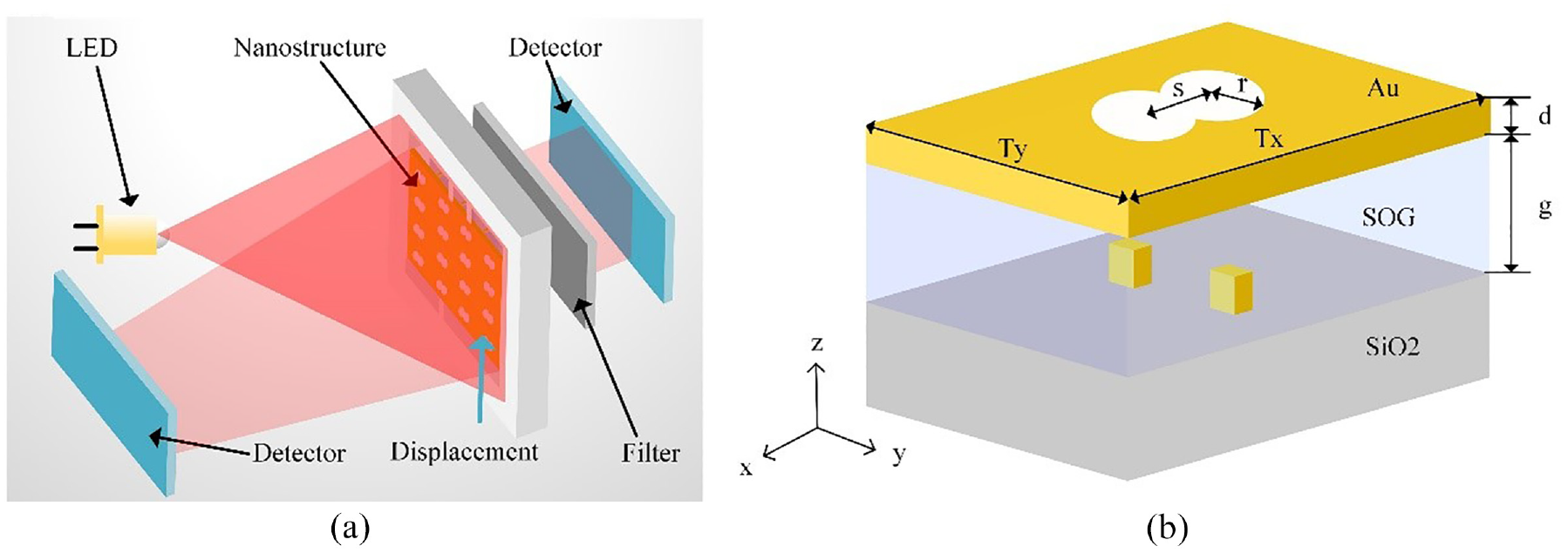
(a) The working schematic of displacement measurement. (b) The unit cell of the plasmonic structure.
Anapole modes of the nanostructure
Figure 1(b) shows the schematic diagram of the proposed periodic nanostructure with period (T). In a unit cell of the structure, two gold (Au) blocks (height h = 100 nm; side w = 50 nm, separated by 300 nm (center-to-center)) are placed on top of the SiO2 substrate. Au film (thickness d = 100 nm) with two nanoholes (radius r = 75 nm, center-to-center separation s = 120 nm) is covered on a layer of spin-on-glass (SOG) of thickness (g). The optical field transmission of the nanostructure is calculated by the FDTD method. The periodic nanostructure is illuminated by a plane wave. The material data of Au used in the simulations are taken from the Johnson and Christy (1972) and permittivity of SiO2 is referred from Palik’s handbook. The refractive index of the background material is set as 1.33 with consideration of practical applications. The mesh size for simulation domain is 2 nm.
Figure 2(a) shows the reflection/transmission spectra of the nanostructure excited by y-linear polarized light. For the nanostructure with Tx = Ty = 600 nm, g = 250 nm, a minimum reflection can be seen at λ = 906 nm, while the transmission is peaked at 903 nm. The peaks are shifted to shorter wavelength as Ty = 550 nm. Without loss of generality, the period in the x and y directions is chosen as the same in the following discussion. Figure 2(b) shows the optical spectra of the nanostructure with rounded edges (with radius re) and rounded corners (rc), and different background medium. It shows that the plasmonic resonance wavelength shifts slightly to longer wavelength for surrounding medium with bigger refractive index. When comparing the peaks, the spectra reveal that the round-corner nanoblocks show a shift to lower wavelength. This blue shift of resonant wavelength is caused by reduced size of the nanoblocks and electron charge distribution.
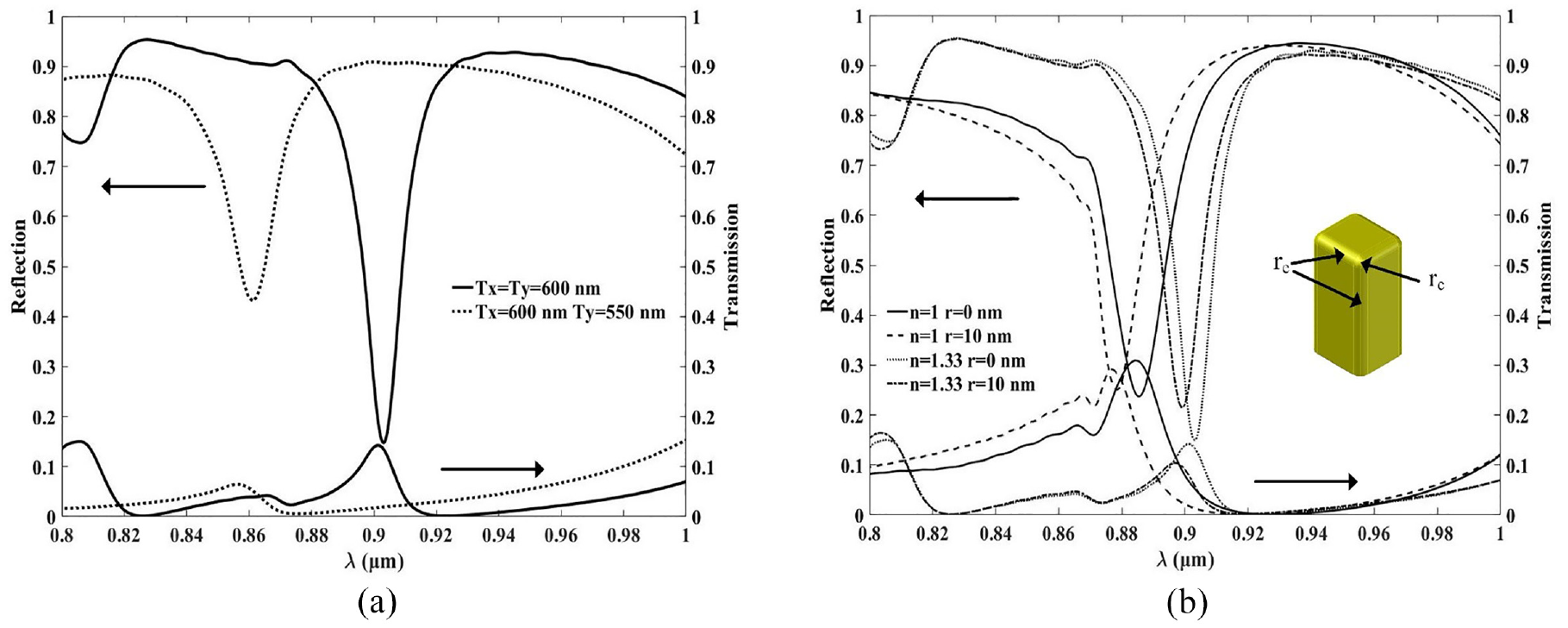
Transmission and reflection of the periodic structure: (a) With different period Tx and Ty and (b) different background medium with refractive index n = 1, 1.33, and nanoblocks with rounded edges r = 0, 10 nm.
A nonradiating anapole mode could be produced by the destructive interference between toroidal and electric dipoles which leads to a minimum extinction spectrum of the structure. Figure 3(a) and (b) shows the distribution of the magnetic field induced in the unit cell of the nanostructure at λ = 905 nm, confirming that a toroidal magnetic mode is generated. As shown in Figure 3(c), the electromagnetic field energy is significantly enhanced in the near-field at the toroidal resonance wavelength. Figure 4 shows that misalignment of the layered structures (e.g. displacement along the y directions, Δy) can significantly change the electromagnetic field distribution and extinction spectra which will be discussed in the next section. It is noticed that the electromagnetic field energy is confined in the DNHs aperture and the dielectric gap layer, so that the electromagnetic field localization could be used for improving sensor design.
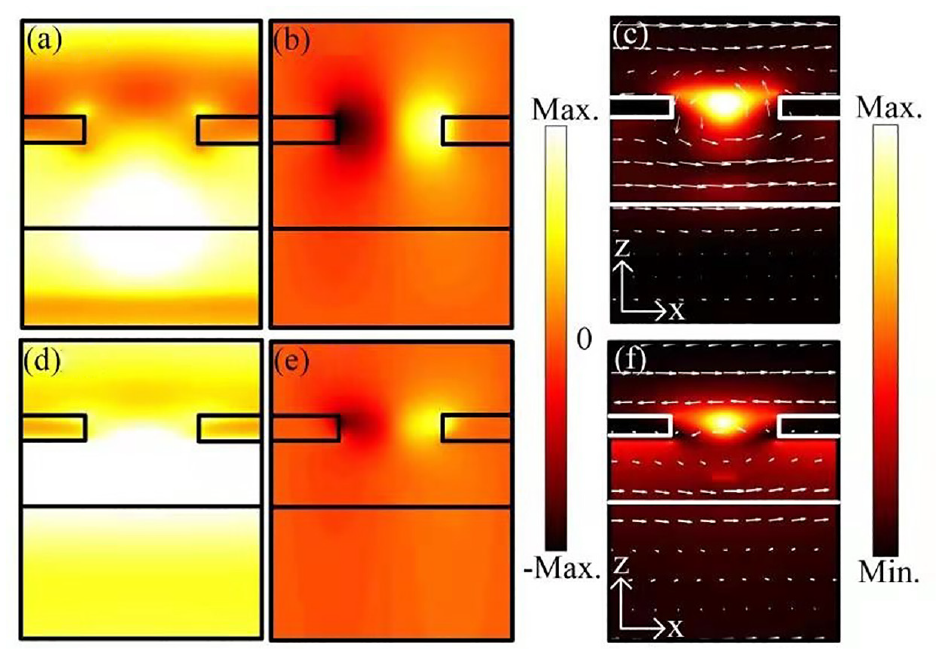
Magnetic field distributions and electromagnetic energy of the structure at (a, b, c) 905 nm and (d, e, f) 876 nm, respectively. (a) Hx at Δy = 0 nm, (d) Hx at Δy = 120 nm, (b) Hz at Δy = 0 nm, (e) Hz at Δy = 120 nm, (c) electromagnetic energy at Δy = 0 nm, (f) electromagnetic energy at Δy = 120 nm. The arrows indicate the magnetic field.
Electric field distributions |
The anapole mode can be easily tuned by varying the geometrical parameters of the structure. The anapole mode wavelength is shifted to longer wavelength as the period T of the structure is increasing (Figure 5). However, the reflection is increased as T is decreased from 600 to 550 nm because the plasmon resonance is coupled stronger between adjacent structures. Nevertheless, the anapole wavelength is not significantly shifted as g increased from 200 to 300 nm. But the reflection is greatly increased with increasing g to 500 nm, indicating that the anapole mode is no longer supported because of weak interaction between the two layers. One new reflection peak is observed at 850 nm, which is resulting from plasmon resonance mode coupling between neighboring structures (Li et al., 2014). The plasmon mode coupling can be clearly seen from the electric field distribution shown in Figure 4(a).
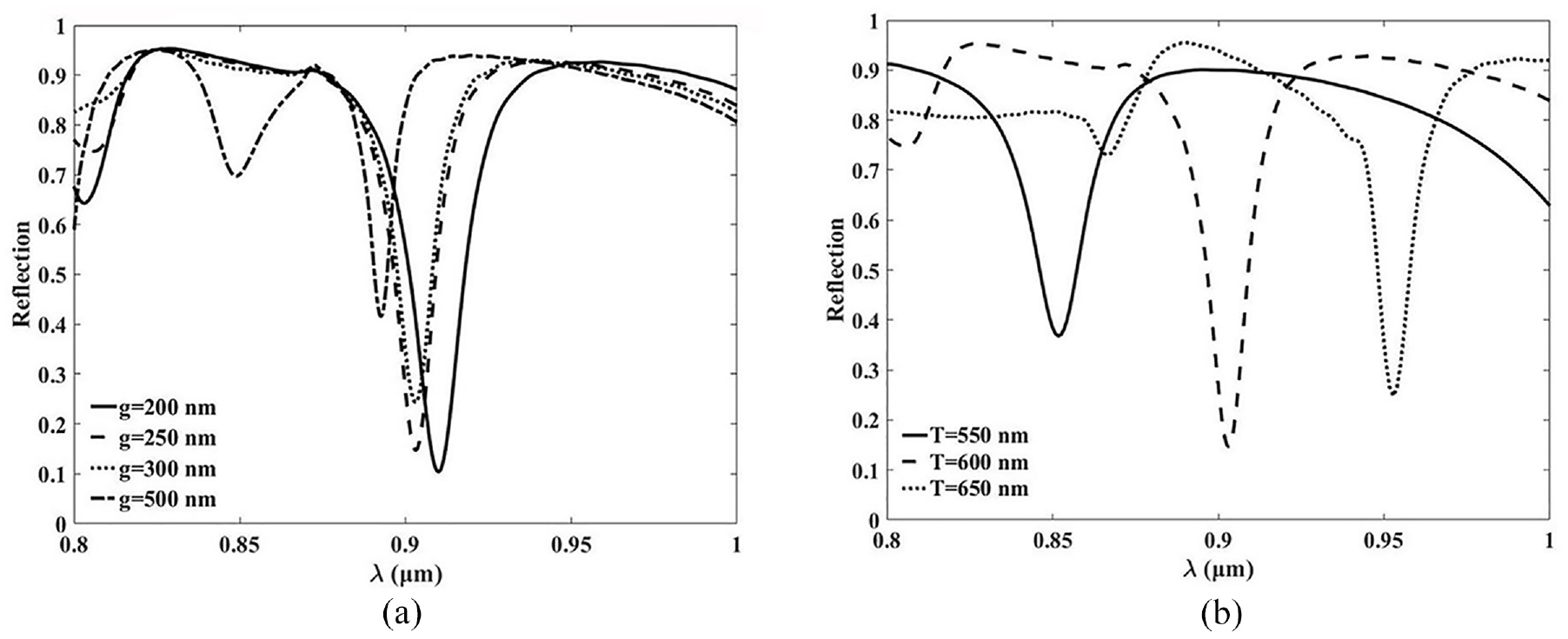
Reflection spectra of the structure: (a) Different SOG thickness, g and (b) different period, T.
Displacement sensitivity
To study the displacement sensitivity of the structure, the periodic nanoblocks are shifted along the x and y directions. As shown in Figure 6(a), the reflection/transmission spectra are not significantly changed while the structure is shifted along the x direction for the y-polarization excitation. However, the spectra are very sensitive to the y direction displacement Δy. There is a new minimum reflection peak around 875 nm, R1, which is decreased from 0.9 to 0.04, as Δy is changed from 0 to 120 nm (Figure 6(b)). Meanwhile, the anapole resonance peak R2 is increased from 0.18 to 0.84.
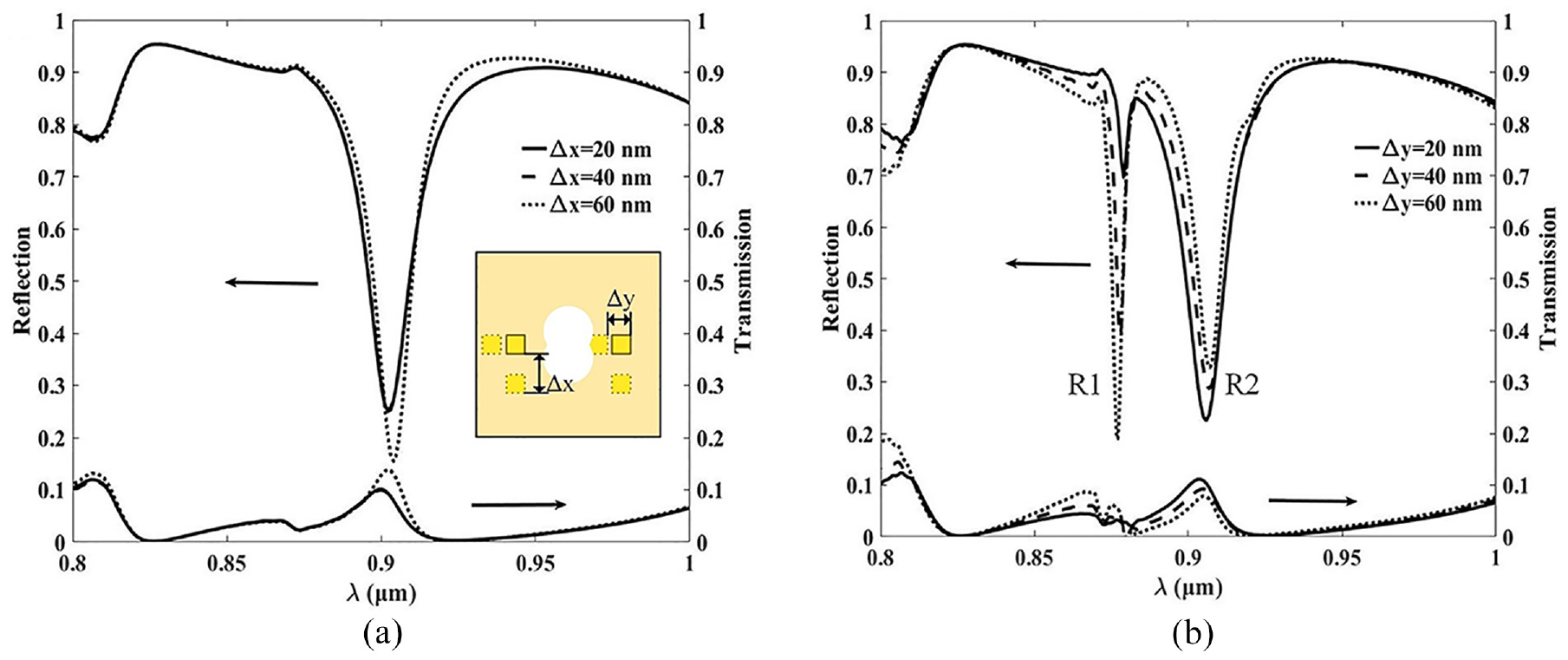
Reflection and transmission spectra as the DNHs and nanoblocks are misaligned. (a) Displacement in the x direction, Δx and (b) displacement in the y direction, Δy.
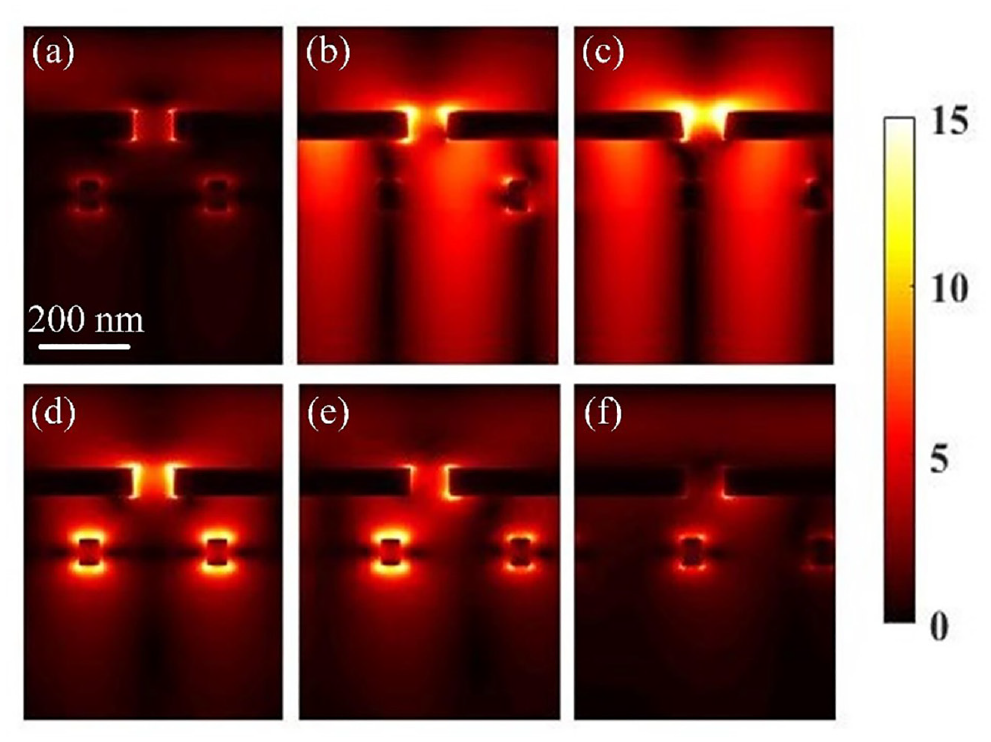
Resonance mode variations induced by displacement Δy can be observed from Figure 4. As Δy is increasing, the electric field |
The reflections R1 and R2 are plotted as a function of Δy in Figure 7. It can be seen that R1 is strongly negatively correlated with R2. While R1 is monotonously decreasing, R2 shows sudden decrease at certain Δy values (30 nm, 60 nm, etc). This is resulted by the electromagnetic interaction between the DNHs and the nanoblocks, as shown in Figure 4. When Δy = 0 nm, the two nanoblocks interact with the DNHs symmetrically. As Δy is increasing, the DNHs interact stronger with the nanoblock that is moving closer to it. While Δy = 60 nm, this nanoblock is interacting with both the intersection tips and the other nanoblock is mainly coupled to the interface between the Au film and SOG (Figure 4(e)). Although R2 is not monotonously changing, the displacement Δy can still be determined by measuring R1 and R2. In Figure 7(b),
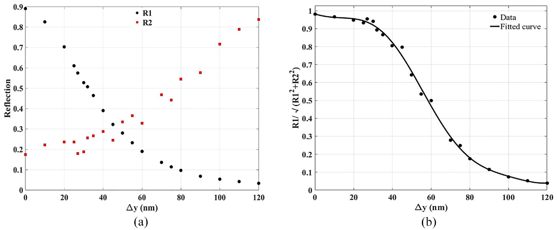
(a) Reflection peaks R1 (anapole mode) and R2 as a function of displacement Δy. (b)
Conclusion
Optical anapole modes in the proposed structure could be readily tuned by changing the geometrical parameters according to practical applications such as nanometrology, biosensors, and microelectromechanical systems. The high sensitivity of displacement of the structure offers more freedom for designing novel sensing devices. Our results show that up to a few hundreds of nanometers displacement could be well determined by detecting the far-field refection spectra under normal illumination. The inverse relationship between two reflection peaks of more than 90% variations allows easy signal processing to obtain precise nanometric displacement.
Footnotes
Declaration of conflicting interests
The author(s) declared no potential conflicts of interest with respect to the research, authorship, and/or publication of this article.
Funding
The author(s) received no financial support for the research, authorship, and/or publication of this article.