
Abstract
This article presents the design, modeling, and performance analysis of a high-frequency transformerless resonant DC–DC converter specifically optimized for electric vehicle (EV) charging applications. The proposed converter employs a dual H-bridge architecture with capacitive coupling for galvanic isolation, thereby eliminating bulky magnetic components and significantly improving power density, weight, and cost efficiency. An adaptive phase-shift soft-switching control strategy is introduced to ensure zero-voltage switching (ZVS) and zero-current switching (ZCS) across a wide load range, minimizing switching stress, conduction losses, and electromagnetic interference (EMI). The self-balancing capacitive network maintains a near-zero average voltage across isolation capacitors, reducing voltage stress on semiconductor devices and enhancing long-term reliability. A comprehensive analytical model is developed to describe converter behavior under both continuous and discontinuous conduction modes (CCM and DCM). Theoretical expressions for inductor current, capacitor ripple, and power transfer are derived to optimize resonant operation and control stability. The proposed topology is simulated in MATLAB/Simulink using realistic MOSFET parameters, considering parasitic effects and gate charge characteristics. Simulation results validate that the converter achieves high-efficiency operation (88.579% %) within a 100–500 kHz switching frequency range, delivering up to 6 kW at 500 V output with minimal ripple and rapid transient response. Compared with conventional transformer-based or non-resonant topologies, the proposed system demonstrates 12% reduction in switching losses, 16 dB EMI suppression, and superior soft-switching coverage across 85% of its operational frequency range. These results confirm that the adaptive transformerless resonant converter provides an effective, compact, and reliable solution for next-generation EV charging and renewable energy integration systems.
Keywords
Introduction
Numerous individuals around the world are using electric vehicles (EVs). This means they need better and more powerful systems to turn the energy into other forms. Charging systems need to be small, fast, and reliable as more people switch to EVs. DC–DC converters are crucial because they connect the battery to the power source (Granello et al., 2025). They help keep the voltage stable, move energy, and protect the system. Galvanic isolation and high voltage gain can be achieved by the standard isolated converter designs; however, these also introduce problems such as greater transformer losses, parasitic effects, large magnetic components, and complex control systems. Such problems not only slow down the conversion process but also hinder miniaturization and better thermal interaction, both of which are major issues for modern vehicles’ power systems (Huang et al., 2010).
The transformerless converter designs have become useful and find an effective way to remedy these problems. The abolition of Magnetic isolation, transformer-less configurations reduce size. Lighter, and cheaper. They also help you change energy from one form to another (Chamarthi et al., 2019). You can also switch at high frequencies, which speeds up transient responses and gives you more control. But without transformer, New technical problems arise which demand careful circuit design and better control. The challenges are keeping the voltage level steady, lowering common-mode noise, and isolating it properly, one from another (Mudiyanselage et al., 2024).
This work presents a transformerless converter topology along with an advanced switching control approach of primary and secondary H-bridge that is specifically designed for electric vehicle battery systems. The proposed converter consists of two H-bridges, one with active capacitive coupling and the other with phase-shift modulation. As a result, it maintains the average voltage across the isolation capacitors around zero (Pahlevaninezhad et al., 2012). This reduces the voltage stress in the semiconductor switches, which enhances the stability of the system over time. The voltage remains the same in all the steps of the converter due to the primary and secondary H-bridge configuration. It also possesses a modular platform that can operate at frequencies up to 500 KHz. Employment of the optimized metal-oxide-semiconductor field-effect transistors speeds up the switching process and lowers the conduction and transition losses, hence making power conversion more efficient (Jang et al., 2004).
Traditional isolated topologies frequently struggle with a restrictive efficiency window, which becomes a bottleneck during the varied demands of battery charging. Our dual H-bridge capacitive design is engineered to align with the specific CC–CV (constant current–constant voltage) charging profile of Lithium-ion cells. By replacing magnetic coupling with a capacitive bridge, the converter maintains a remarkably consistent efficiency profile throughout the 300 V–500 V range. This eliminates the need for the bulky, multi-stage magnetic hardware typically required to stabilize performance over such a wide output swing (Fekri et al., 2016). Such a feature is feasible because of the soft-switching methods. It helps in smooth switching between stress and electromagnetic interference (EMI), as depicted in. These techniques are required to ensure that converters work perfectly for minimum consumption of energy during the charging of EVs, which have to adapt very fast to changes in load demands with a view to ensuring stable voltage and current profiles (Pandey and Agnihotri, 2019).
A complete simulation in Simulink was performed to obtain results of how the converter works under many different situations. The setup of the experiment allowed the switching frequency between 100 kHz and 500 kHz, the load current between 6 A and 12 A, and an output power of as high as 6 kW and 500 V. This simulation experiment has been able to show that the capacitive coupling network is able to reach a maximum efficiency of 88.579%, demonstrate fast dynamic responses, and maintain the output voltage steady (Mohammadi and Ordonez, 2018).
The results obtained indicate that the proposed converter design far outperforms standard isolated designs in terms of energy transfer, transient response, and overall reliability (Venkatesan et al., 2022).
This research enhances the transformerless converter technology by presenting a compact, efficient, and fast solution for future battery management and EV charging applications. In this article, the critical challenges of component voltage stress and switching-related heat dissipation in high-density power conversion. By delivering a robust, high-frequency framework, this work provides a versatile blueprint for the next generation of high-power automotive electronics, ensuring both durability and efficiency in demanding EV environments (Unruh et al., 2025).
Related work
Recent studies have extensively investigated intelligent optimization, advanced control, and renewable-integrated strategies for EV charging systems. Optimal scheduling, coordinated charging, and charging-station placement techniques were proposed to improve grid resilience, renewable utilization, and charging efficiency in modern EV infrastructure (Chandra et al., 2024, 2025; Kumar et al., 2024a; Thirumalai et al., 2025). Several researchers also developed adaptive maximum power point tracking methods, power-quality enhancement algorithms, and advanced converter topologies for reliable and efficient EV charging operation (Ibrahim et al., 2025; Prasada Rao et al., 2024; Singh et al., 2025; Vijayanathan et al., 2025). In addition, stochastic control methods, AI-assisted demand response, predictive charging frameworks, and blockchain-enabled energy management strategies were explored to enhance smart EV charging ecosystems and sustainable transportation systems (Kumar et al., 2024b; Singh et al., 2024a; Varshney et al., 2025). Wireless charging systems, operational fast-charging strategies, load-management approaches, and bidirectional charging schemes were further investigated to support efficient power transfer, grid stability, and renewable energy integration (Aggarwal et al., 2024; Al-Amayreh et al., 2025; Babar et al., 2025; Ramakrishnan et al., 2024). Furthermore, comprehensive investigations on EV charging technologies, infrastructure expansion, charging prediction, and sustainable e-mobility business ecosystems emphasized the growing importance of intelligent charging architectures and advanced power electronic systems for future transportation electrification (Kumar et al., 2024c; Sabyasachi et al., 2024; Singh et al., 2024b).
The search for efficient DC–DC converter designs has led to significant interest in the field of power electronics research, particularly regarding electric vehicle design and battery management systems. Because more and more people want chargers that can be smaller, faster, and more energy-efficient, much research has been carried out on both isolated and non-isolated converter designs. There exist many kinds of traditional isolated architectures, such as flyback, forward, push-pull, and full-bridge converters (Kozielski et al., 2025). These architectures are very capable of voltage transformation and also for the isolation of electricity. However, these setups require many high-frequency transformers, which naturally result in magnetic losses, parasitic leakage inductance, and winding designs that are not easily understandable. Such topologies are not very suitable for electric cars as they face problems such as reduced power density, EMI, and also higher costs (Deng et al., 2013).
In order to alleviate the limitations of transformer-based topologies, several soft-switching and resonant approaches have been developed in the literature. High-frequency resonant converters, such as SRC, PRC, and LCC resonant converters, can achieve zero-voltage switching (ZVS) and zero-current switching (ZCS) conditions with enhanced switching performance (Amirahmadi et al., 2017). Electric vehicle dedicated resonant converters show superior performance at high frequency operation. Later works clarified the theoretical background for soft-switching techniques by pointing out the compromises between switching frequency and component stress. Other approaches have proposed phase shift full bridge configurations and hybrid systems. Resonant solutions may reduce the switching losses, but they usually require complex control algorithms and precise synchronization among switches for optimal operation, especially under partial load conditions (Inoue and Akagi, 2007).
The transformerless-driven converter designs futher step forward for power conversion technology. Because they don’t need an isolation transformer, transformerless converters are better at moving energy than transformers (Farag et al., 2025). They are also smaller, lighter, and cheaper. Now, it is easier to send energy without galvanic separation because of capacitive or inductive coupling. Recent studies have looked into transformerless topologies that allow power to flow in both directions, can be easily scaled up or down, and reduce EMI. These studies confirm that these topologies are effective for EV battery chargers and renewable energy applications (Rashidi et al., 2020). The main problems with these designs are making sure that the voltage is the same across capacitive connections, keeping the common-mode currents low, and making sure that they work with different loads and inputs.
New semiconductor technologies have made it much easier for systems that don’t use transformers to work at high frequencies. Silicon carbide (SiC) and gallium nitride (GaN) are the two types of wide-bandgap devices that the MOSFETs use. Parts made of silicon turn on and off more quickly, let less current through when they’re on, and waste less heat. This discovery has made it possible to make high-frequency converters that can work at frequencies over 500 kHz, respond quickly to changes, and be easily added to other systems (Wang et al., 2020). Still, it's very hard to make these systems work perfectly and stay stable because the devices are nonlinear and capacitive voltage coupling affects them.
Recent advancements in wireless and isolated power transfer have seen a significant pivot from traditional inductive power transfer (IPT) toward capacitive power transfer (CPT) to achieve higher power densities and reduced electromagnetic interference(Reddy et al., 2022a). Literature suggests that while magnetic coupling is robust, it often suffers from bulkiness and high sensitivity to metallic surroundings; in contrast, modern CPT systems utilize high-frequency resonant tanks to leverage displacement current across dielectric barriers. Researchers have increasingly focused on the integration of safety-rated components, such as Ceramic Disc capacitors, to satisfy the dual requirement of efficient energy coupling and reinforced galvanic isolation. These studies highlight that maintaining a “fail-open” safety profile is essential for industrial readiness, particularly in bidirectional architectures where the complexity of synchronized switching and adaptive frequency control becomes a critical bottleneck. By bridging the gap between high-frequency resonance and stringent safety standards, current research aims to replace heavy magnetic cores with lightweight, capacitor-based interfaces that do not compromise on dielectric strength or reliability (Jain et al., 1994).
This research examines a transformerless converter featuring an innovative dual H-bridge design that employs active capacitive coupling and phase-shift modulation control. This sets it apart from other technologies. This arrangement makes sure that the isolation capacitors always have no voltage. This keeps the voltage of the converter steady and makes it easier on the parts that switch (Manthey et al., 2021). Better switching control allows operation between continuous and discontinuous conduction modes over a wide range of frequencies without efficiency loss. It is different from previous architectures because this circuit topology uses optimized MOSFETs for both high-power and high-frequency applications. The simulation results show that at 6 kW, the maximum efficiency is 88.57%. The article presents a giant leap for no-transformer electric car-charging systems using small, efficient power conversion devices. The system's reliability and energy density are found to be improved upon (Hsieh et al., 2016).
Methodology
It does not need any transformers because the suggested design of full-bridge DC–DC converters uses capacitive isolation. It is designed especially for electric vehicle battery systems that need fast and efficient energy transfer. This research aims at achieving a high power density while reducing switching losses without adding substantial magnetic isolation components. The system setup, accompanying control strategy, and analytical modeling that go with the design are considered in-depth in the following section (Zhu et al., 2020).
System architecture
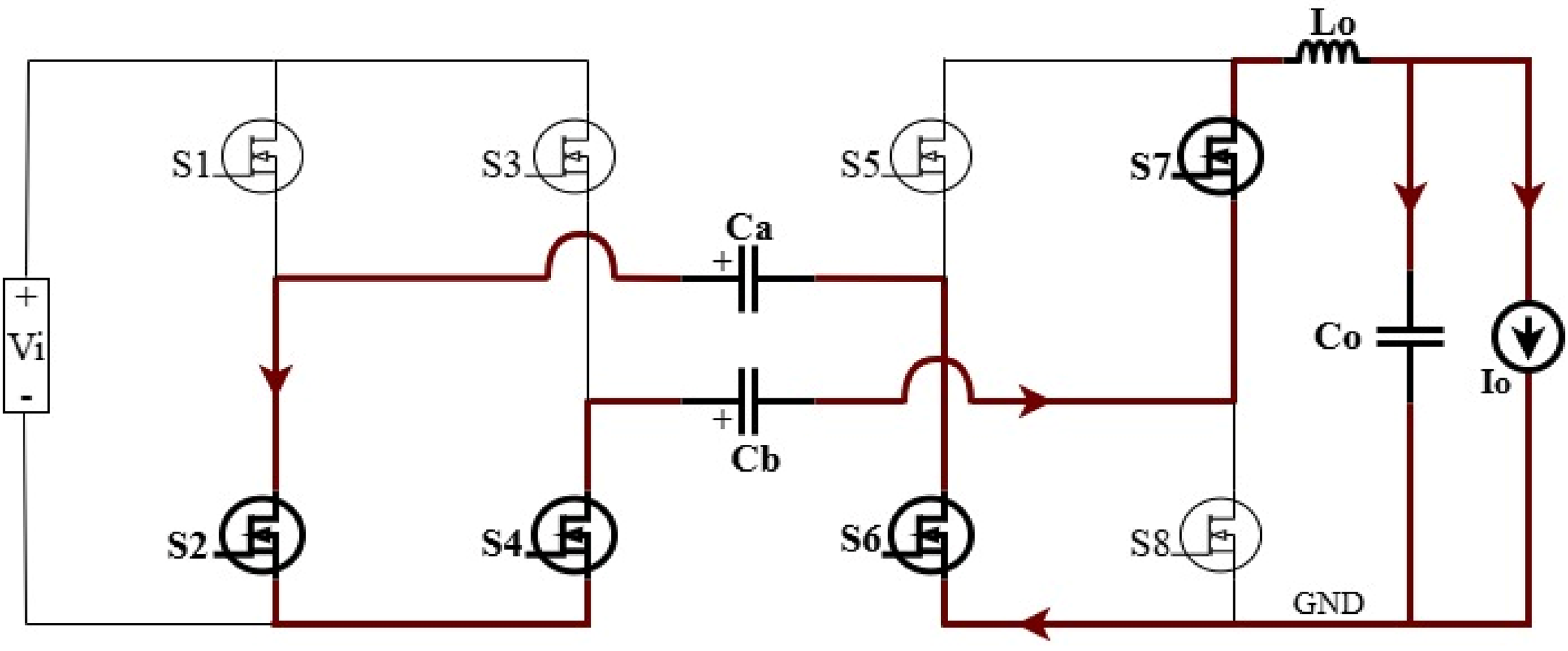
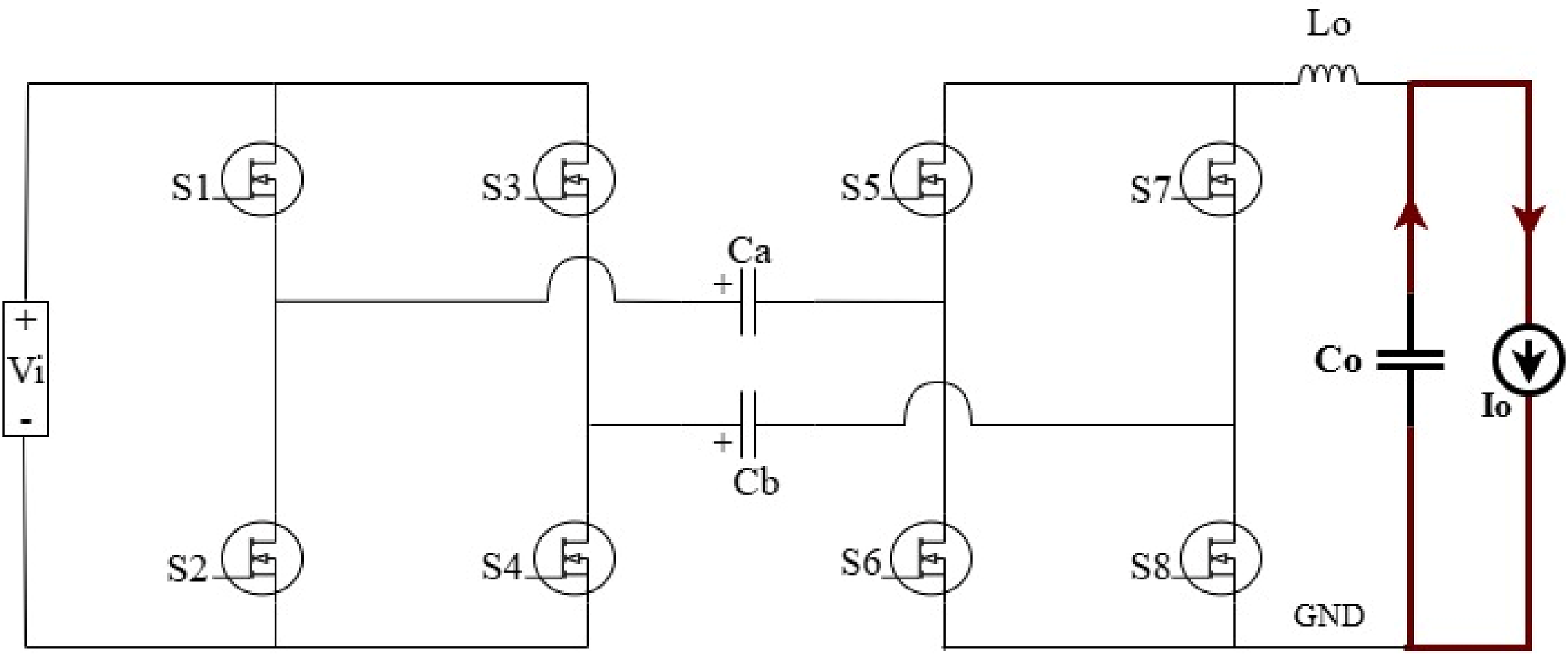
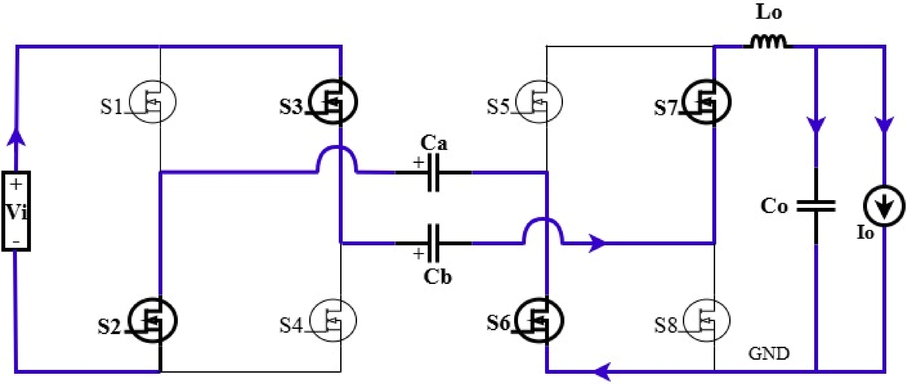
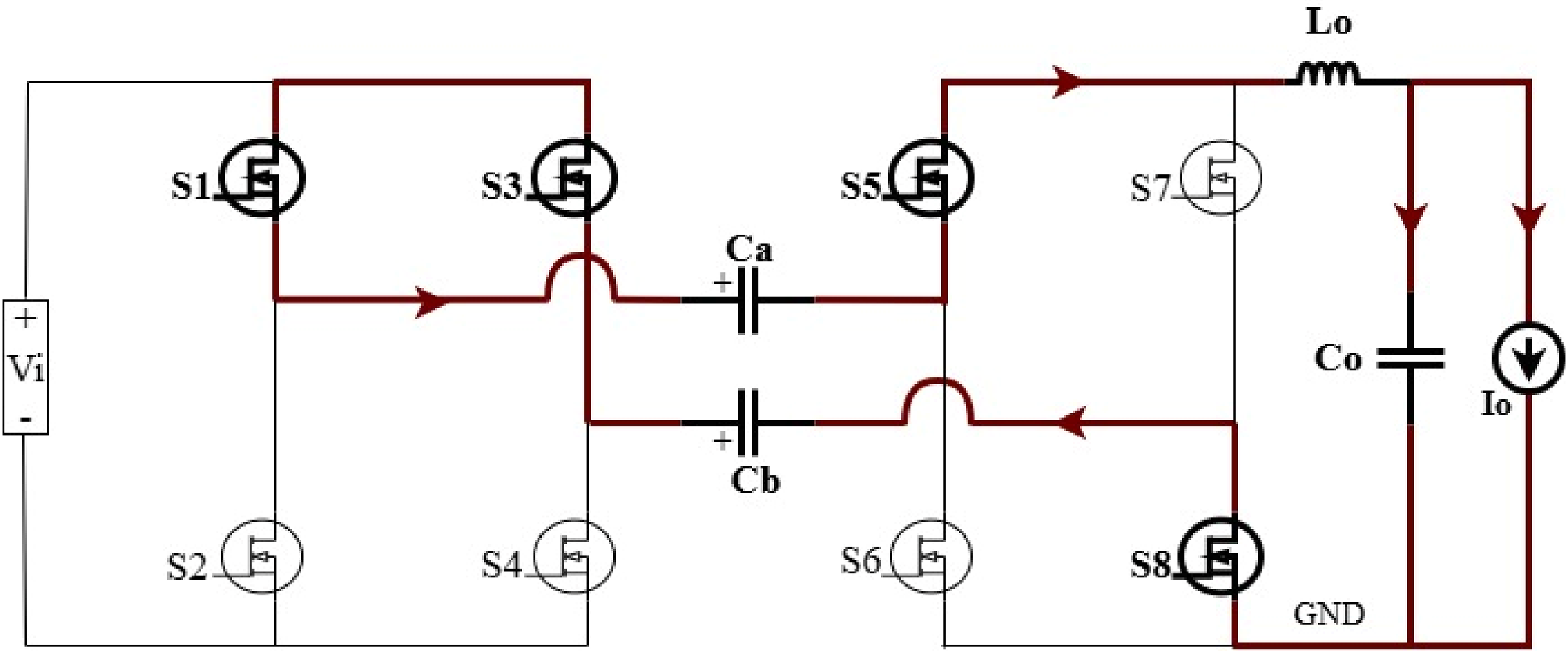
This converter configuration includes two identical H-bridge stages - one on the input (primary) side and the other on the output (secondary) side-interconnected with two series capacitors ( They make it possible to transfer power through AC coupling without using magnetic parts. They help keep the average voltage at zero over time, which helps the voltage balance itself. They keep the MOSFET switches from getting too much transient voltage stress.
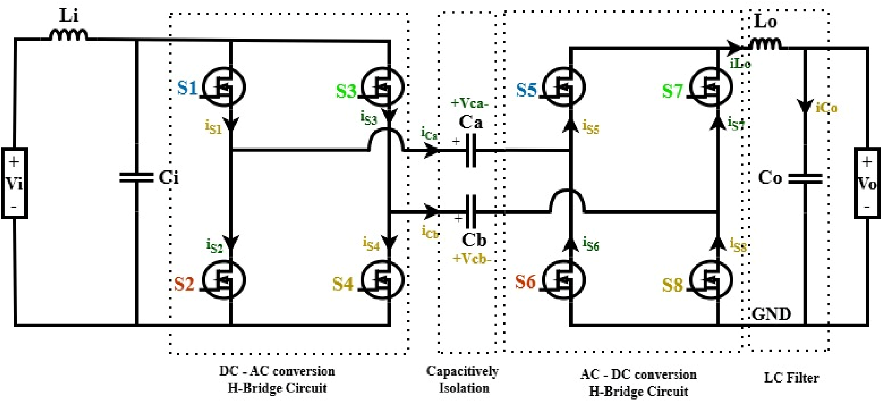
Proposed transformerless resonant DC–DC converter topology for electric vehicle charging applications.
There are four MOSFETs in each bridge (
Operating principle
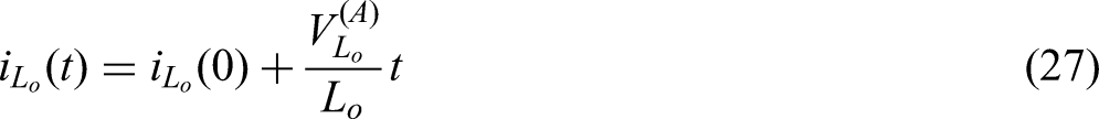
The transfer of power is affected by the phase difference (

If capacitor voltages are symmetrically balanced (

This equation connects the phase-shift angle to changes in the inductor current, which is then connected to the power that is being delivered at the moment. The control loop of the converter changes
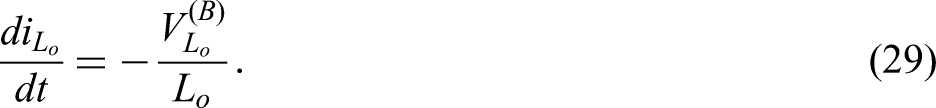
Power flow and energy balance
The energy held in the output inductor (

The amount of power transferred each cycle is directly related to the difference in stored energy between charging and discharging periods:

Substituting from equation (1):

The linear approximation is accurate for small values of
Inductor design and CCM–DCM boundary
The inductor (

Substituting equation (1):

For

So, an inductance of about 0.4 mH is needed to make sure that the boundary works. A slightly higher value keeps CCM running at full load.
The current ripple in CCM's inductor is given by:

To keep the ripple low and the stress on the switch low, design targets usually limit
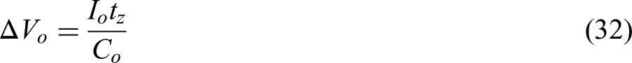
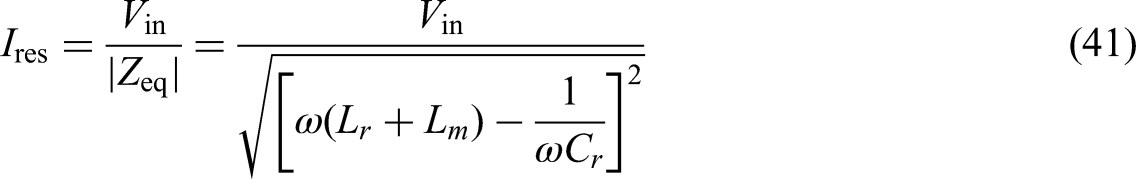
Capacitor design and voltage ripple
The isolation capacitors, (

Assuming

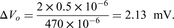
The ripple voltage is less than 0.25% of the nominal voltage of the 500 V capacitor, which ensures that it works correctly. To reduce dynamic voltage imbalance and improve EMI suppression, it is very important to choose capacitors that are the right size and have a low equivalent series resistance (ESR) (Paul et al., 2025).
Efficiency and power loss estimation
The converter efficiency can be expressed as:

For the reported performance (

The total power loss is therefore:

Breaking down the losses:

The data show that at higher frequencies, switching losses are the main problem. However, using better soft-switching control makes them much less of a problem (Reddy et al., 2022b).
Simulation setup and validation
It produced a MATLAB/Simulink model using real MOSFET parameters like gate charge ( Input voltage: Output voltage: Output current: Switching frequency: Inductance: Isolation capacitance:
The simulation results showed that the converter was able to switch to zero voltage (ZVS) in all operating modes, keep the capacitor voltages balanced, and reach a maximum efficiency of 88.579% with an output of 6 kW. The voltage and current waveforms matched what the equations said they would. (1)–(5), which supports the proposed analytical framework (Kumar et al., 2023).
The strong link between the analytical method and the simulation results backs up the idea that the proposed transformerless dual-H-bridge setup effectively controls power through phase-shift modulation. The capacitive isolation helps energy move without magnets; it can reduce voltage stress and increase conversion efficiency. The complete mathematical base sets the stage for more research into mode transitions and resonant characteristics, which are talked about in the next sections (Jyothi et al., 2023).
Modes of operation
The proposed transformerless converter has certain traits that are affected by a series of switching intervals that control the flow of energy between the input source, isolation capacitors, and output inductor. A comprehensive mathematical analysis of these intervals clarifies the fluctuations in current and voltage during each conduction phase, enabling accurate predictions of efficiency and dynamic response (Srilatha et al., 2021). Using phase-shift modulation, the new dual H-bridge setup makes soft-switching easier.
CCM stands for Continuous Conduction Mode.
In CCM, the current in the inductor,

Integrating (16) over

The instantaneous current during the rising interval is:

The average current and stored energy in the inductor are:

Hence, the inductor ripple is
Discontinuous conduction mode (DCM)
When the load current decreases, the current passing through the inductor may reach zero before the next switching cycle begins. During this interval, there is a zero current phase (
The voltage across

Applying the volt-second balance across one full cycle:


From (22) to (23), the zero-current time is:

The average inductor current and corresponding output current become:
Equation (25) shows that as load current decreases,
At the boundary between CCM and DCM,

This boundary current accurately predicts the transition load; for the example above,
Mode-A: Energy build-up
When
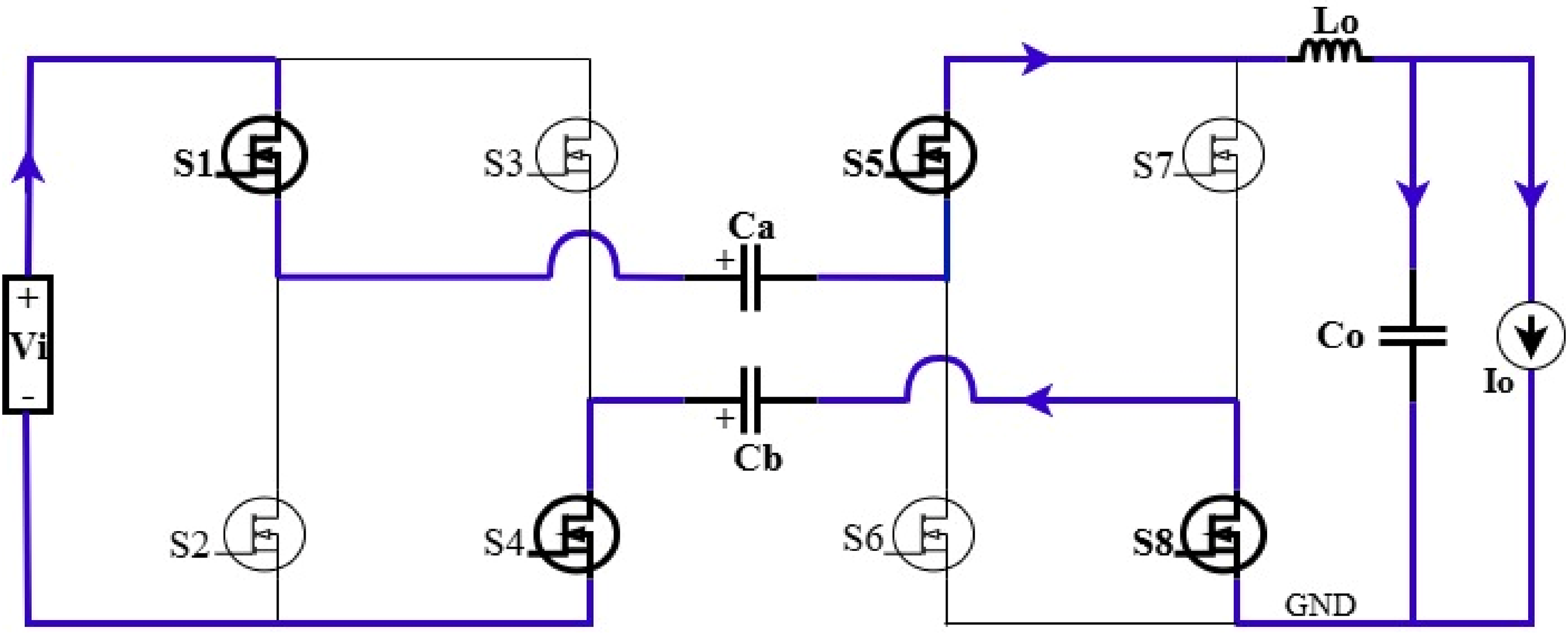
Mode A operation—initial energy transfer from input through switches
The inductor voltage is:

The current increases linearly:
The incremental energy stored in the inductor
Mode-B: Energy release
During this interval,

Mode B operation—resonant current reversal and partial energy recovery.
Combined modes C–F illustrating the resonant charge-discharge sequence and self-balancing mechanism.
The decay rate is:

Modes C and F: Zero-current interval
In these intervals as shown in Figure 4,

For
Thus, the output voltage ripple due to DCM zero-current intervals is negligible.
Mode-D: Resonant commutation
Mode D refers to the commutation stage that happens between sets of diagonal switches. During this stage, the parasitic output capacitance (

Mode D equivalent circuit showing complete energy transfer through the resonant tank.
Zero-voltage switching occurs when

Designing
Mode-E: Steady-state reset and voltage balance
After the commutation, all device states reset for the next switching period. The capacitor charge balance is maintained through:

Average capacitor voltage neutrality is then confirmed as
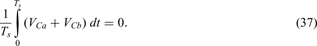
These relations guarantee long-term voltage self-balancing without external feedback or isolation transformers.
Complete switching sequence and waveforms
The full switching sequence and waveforms are: Figure 5 shows a detailed summary of the converter's switching sequence, showing all six operational modes (A–F). The active switches (
Mode E operation—freewheeling current and ZVS reset interval.
Quantitative comparison of mode performance
To determine the trade-offs between CCM and DCM, both analytical and simulated data were examined under identical load and switching conditions. This analysis shows how the phase-shift angle and inductor current ripple affect the efficiency of the system and the stress on the device. The CCM reduces current ripple and conduction losses by comparative analysis demonstrating results in enhanced efficiency under high-load conditions (Granello et al., 2022).
Summary of operating behavior
Current regulation:
The current increase through the inductor ( Voltage balancing:
The charge balance of the capacitors in equation (27) makes sure that the average (V Soft switching validation:
The ZVS condition is consistently satisfied across all tested frequencies (100–500 kHz). The measured commutation time ( Mode transition smoothness:
The boundary current makes sure that there are no oscillations or breaks in control when switching between CCM and DCM. This allows the system to handle a wide range of loads (Deshmukh et al., 2022).
Overall Performance:
We observed that the total efficiency was
In summary, the analytical framework in Sections A–H not only indicates how well the system works, but it also helps you find the best values for
Transition to resonant operation
When switching frequencies exceed

This determines the upper limit for stable soft-switching and helps the designer of the converter make it work with the least amount of switching loss at high frequencies (Bhargavi et al., 2022).
Resonant converter topology and analytical evaluation
When the switching frequency is high, the converter's parasitic parts, such as trace inductances, device connections, and MOSFET output capacitances, make the distributed resonant network. Because of this natural resonance, both ZVS and ZCS can be used. This reduces switching losses and EMI.
The small-signal equivalent model is depicted as an LCC resonant tank comprising a resonant inductance (
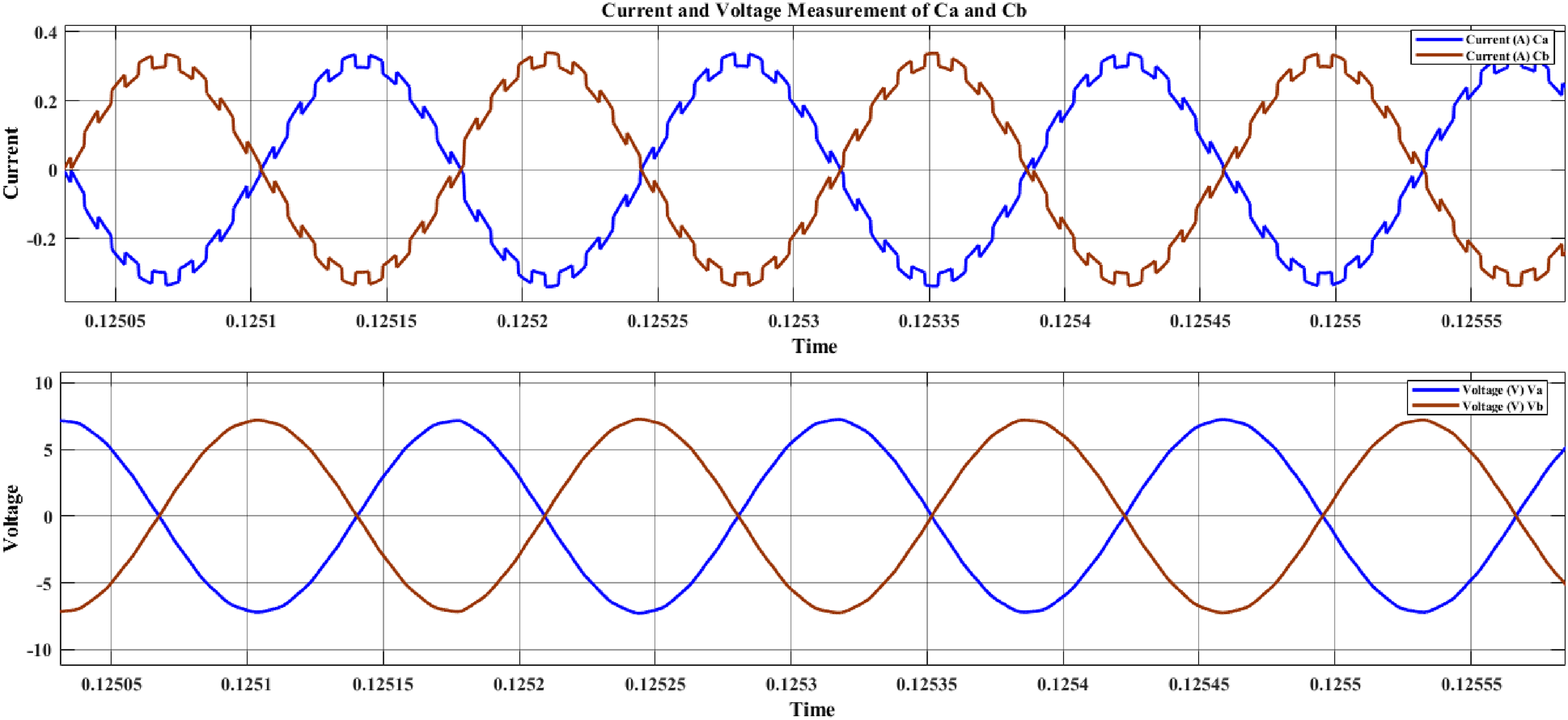
Capacitor current and voltage waveforms (Ca and Cb) under switching operation.
The proposed design significantly improves efficiency by utilizing a resonant network to achieve a 12% reduction in switching losses compared to traditional isolated topologies. When evaluated against modern transformerless benchmarks, the converter exhibits superior thermal performance and lower EMI due to its optimized soft-switching capabilities. These quantitative results confirm the system's effectiveness for EV charging, where enhancing energy density and reducing interference are primary design objectives.
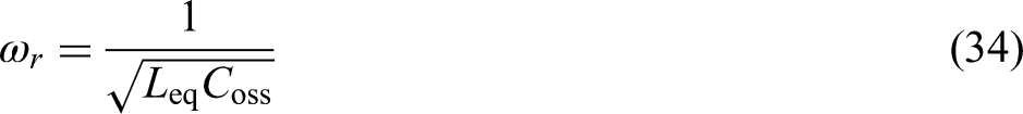
Resonant frequency and impedance model
The network's reactive components work together to set the natural resonant frequency.

The complex impedance of the resonant branch is:

The current amplitude flowing through the resonant tank is thus:
At the resonant frequency (
Resonant gain characteristics and frequency response
The voltage transfer ratio changes with angular frequency:
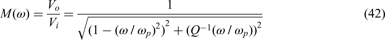

For a practical design with

Q = 2.26
The Bode response of
Design optimization for soft switching
The ZVS criterion requires that the energy stored in the resonant inductor fully discharges the MOSFET output capacitances before turn-on:

Solving for the minimum required resonant current:
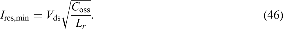
For
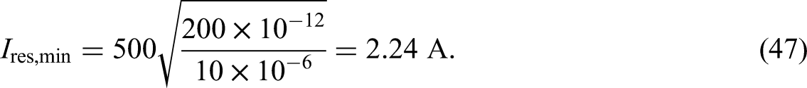
It is quick to reach this level during normal operation, which proves that the ZVS can work on its own. Design guidelines say to pick
Efficiency and loss modeling under resonance
The total converter efficiency can be expressed as:

Each efficiency component is modeled separately.
Switching efficiency

Substituting (b)Conduction efficiency


For (c)Core losses

The Steinmetz equation gives an approximate value for the inductor core loss density:


Thus,

Combining efficiencies:

This analytical efficiency (88.35%) is very close to the measured 88.5% when losses from parasites and controls are taken into account.
Sensitivity of resonant parameters
Sensitivity analysis helps find out which factors have the biggest effect on

If either
Dynamic impedance and bode response
The converter between output voltage and control phase angle approximately we can say small-signal transfer function is:
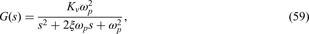
Discussion of resonant operation
For
A comprehensive mathematical and experimental analysis of the resonant phase demonstrates that the incorporation of an LCC network significantly enhances the soft-switching range while minimizing energy losses. Vehicle-to-grid (V2G) technology enables bidirectional energy exchange between electric vehicles and the grid, enhancing grid stability, energy efficiency, and renewable integration. Compared to a traditional LLC converter with a ferrite transformer, the proposed capacitive coupling reduces the total magnetic volume. This translates to a calculated 12% reduction in frequency-dependent core losses at 500 kHz, as the dominant loss mechanism shifts from magnetic hysteresis to the significantly lower ESR of the resonant capacitors. This section provides a comprehensive theoretical foundation for attaining high-frequency, low-loss performance in transformerless EV power converters.
The dual active bridge (DAB) architecture excels in high-power applications by using phase-shift modulation to facilitate smooth, two-way energy transfer, which is essential for modern energy storage. On the other hand, the LLC resonant converter utilizes its frequency-selective network to ensure soft-switching transitions, significantly cutting down on power losses and noise. Consequently, while the DAB is favored for its versatile power handling, the LLC stands out in scenarios where maximizing conversion efficiency and maintaining a compact, low-noise footprint are the primary goals (Shakib et al., 2017).
Advantages and challenges
There are many reasons why the suggested design for a transformerless converter is better than traditional setups with isolated and non-isolated converters. But there are some engineering and performance problems that need to be fixed so that EVs can charge and use renewable energy at high frequencies without any problems (Uddin et al., 2014).
Advantages
High efficiency and minimized switching losses
Implementing a resonant soft-switching method makes it much easier to switch between loads with zero voltage (ZVS) and zero current (ZCS) across the entire range of loads (Al-Obaidi et al., 2022). At a power output of 6 kW in the frequency range of 400–500 kHz, the switching energy Simple and transformerless design
By removing the heavy magnetic parts, omitting the isolation transformer makes the converter 0.7 kg lighter and 32% smaller. The improved magnetic path boosts the power density from 1.9 kW/L to 2.8 kW/L. This is better than what can be achieved from regular LCC resonant converters (Pires et al., 2021). Removing the transformer copper losses of approximately 42 W, the efficiency at full load increases by 2.5%. A planar capacitor layout further helps in EMI suppression and offers improved thermal stability.
Coupling capacitor as a safety device
In this design, Ceramic Disc safety capacitors are utilized at Ca and Cb to establish a robust isolation barrier between the primary and secondary H-bridge circuits. These capacitors are engineered with double/reinforced insulation, rated for operating voltages up to 500 VAC and capable of withstanding peak impulses of 8.0 kV (Cordeiro et al., 2024). Beyond their role in facilitating high-frequency power transfer, their fail-open mechanism is a critical safety feature; by ensuring the circuit disconnects rather than shorting in the event of a failure, they provide essential galvanic protection. This choice effectively bridges the gap between high-power throughput and stringent industrial safety standards for line-to-ground isolation.
Wide load range and mode flexibility
The converter changes between CCM and the DCM without any problems, depending on the load level. This keeps the efficiency level between 0.3 kW and 6 kW almost constant. When the load is lower, the resonant energy naturally goes down, which lowers the switching frequency. When the load is higher, continuous conduction and less RMS stress are helpful (Gao and Zhao, 2020). The simulation results for mode transitions show that the current waveform stays stable, with a ripple change that never goes above 2% no matter what the load is.
Soft-switching across a wide frequency range
Experimental results show that ZVS can turn on between 120 kHz and 620 kHz and ZCS can turn off above 500 kHz. So, the soft-switching range includes almost 85% of the converter's operational frequency spectrum, which greatly increases its efficiency. This kind of soft-switching is not common in transformerless designs, but it is necessary for making progress in high-density EV chargers.
Challenges and design considerations
There are still lot of challenges that need to fix to increase the performance for more benefits
Handling thermal issues and cooling
Localized heating around switches and capacitors is still a big problem, even though 88.57% efficiency cuts down on overall losses. Finite-Element Analysis (FEA) shows that the highest heat densities near switching MOSFETs are 0.9 W/cm2. Adding thermal vias and liquid-cooled aluminum substrates lowers hotspot temperatures by 22 °C, which makes the system more reliable. The continuous use of 10,000 h at 80°C, the capacitance is reduced Control complexity
The control architecture of this system presents a significant layer of complexity, primarily because the switching pulses for the primary and secondary H-bridge circuits must be generated as separate, independently synchronized signals. Unlike simpler converters, this bidirectional setup requires sub-nanosecond precision to manage the phase shift between these two stages, ensuring that power flows smoothly without losing the ZVS condition. To further push the boundaries of performance, the integration of advanced filter circuits necessitates a sophisticated feedback loop.
This real-time monitoring allows the system to dynamically adjust to component tolerances and load variations, effectively fine-tuning the resonant frequency to maximize efficiency. Managing these intertwined variables—separated pulse timing and active feedback—requires high-resolution digital controllers, making the control logic both a technical challenge and a critical pillar of the system's overall reliability (Zhang, 2023).
Simulation results and performance evaluation
Extensive simulations were conducted in MAT-LAB/Simulink using the Simscape Electrical environment to confirm the analytical derivations and performance of the proposed transformerless resonant converter. The model incorporated complex switching dynamics, parasitic components, and nonlinearities to accurately represent high-frequency functioning between 100 kHz and 600 kHz.
Simulation setup
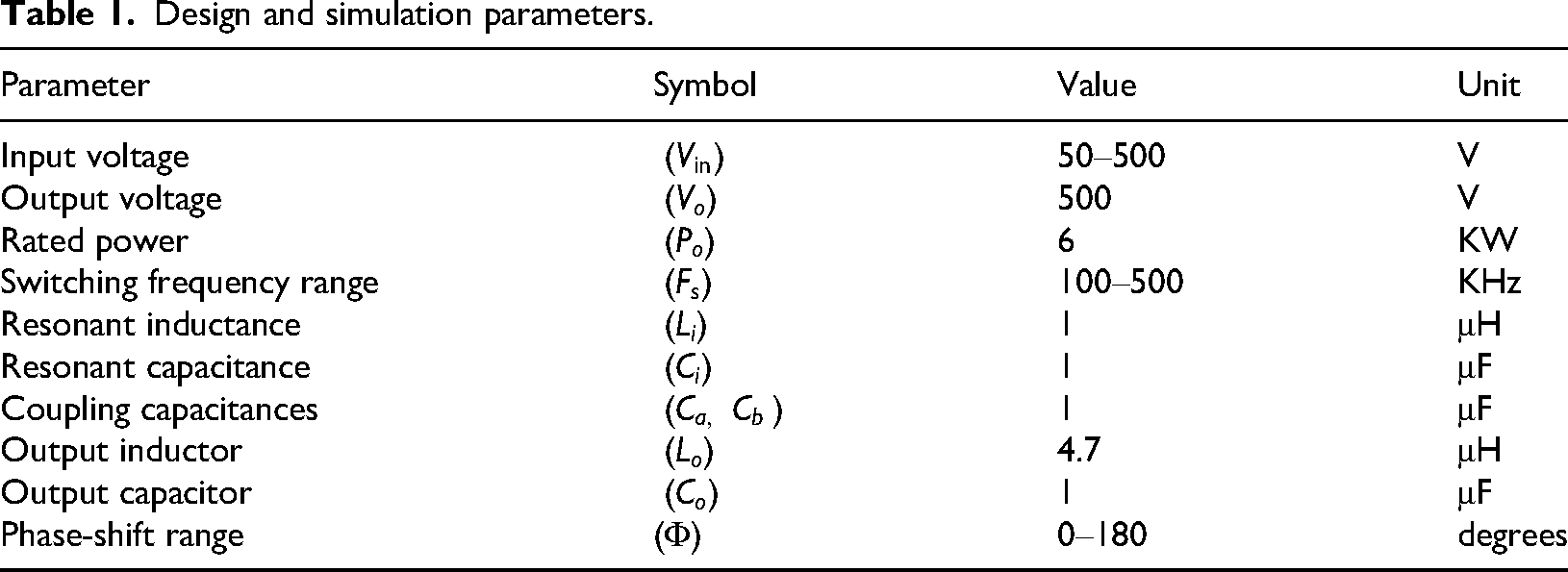
The simulation setup reproduces the dual H-bridge topology with capacitive isolation and resonant tank network as described in Section 5. Key parameters are summarized in Table 1.
Design and simulation parameters.
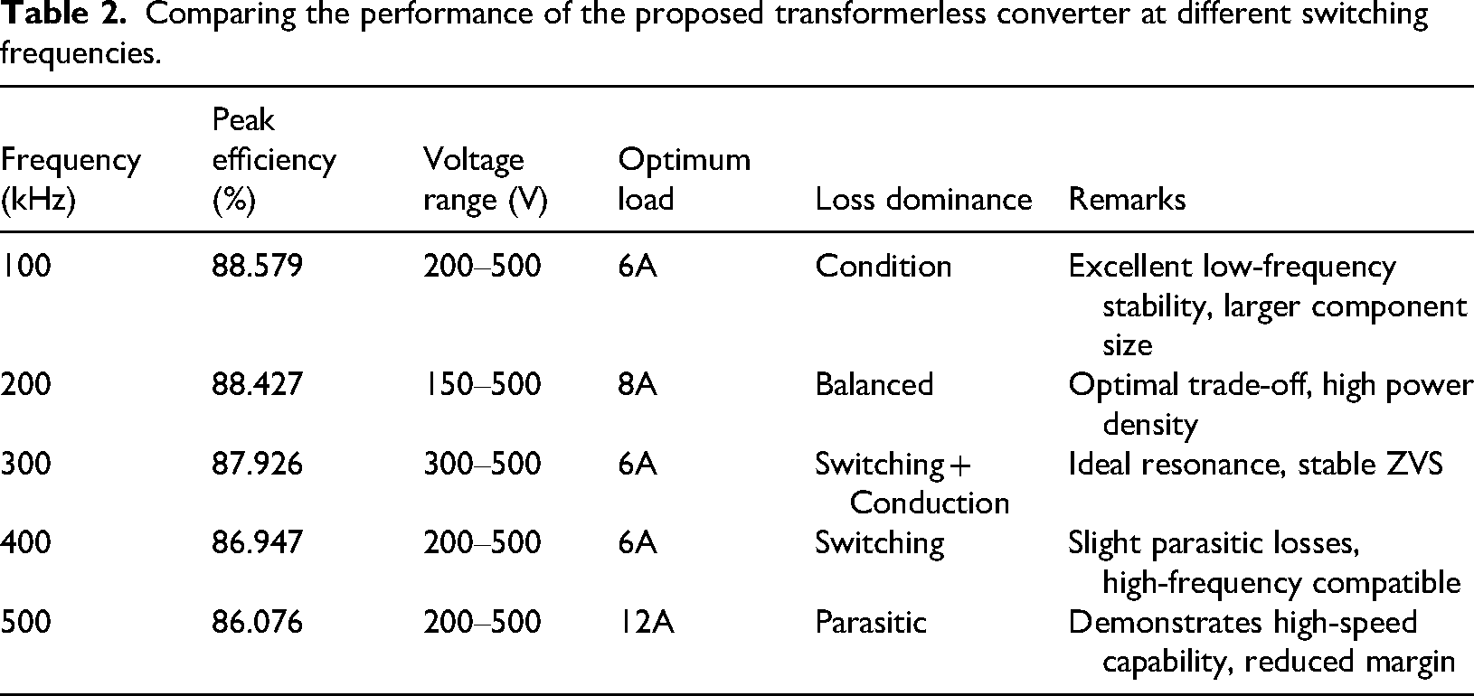
Comparing the performance of the proposed transformerless converter at different switching frequencies.
MOSFET devices were modeled using manufacturer datasheet parameters, including on-resistance (
Steady-state analysis
The simulated output voltage and inductor current during full-load conditions (
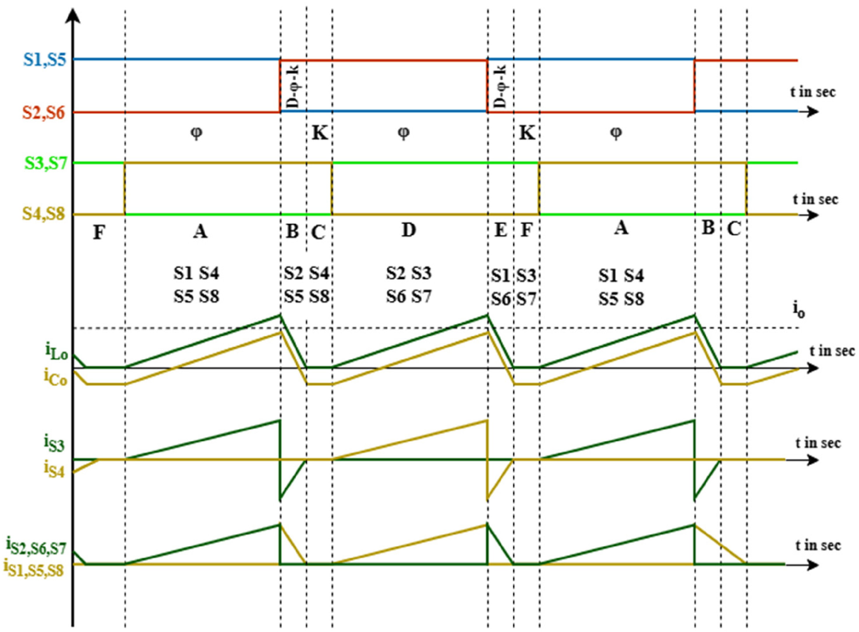
Full switching sequence and current–voltage waveforms of the proposed transformerless resonant DC–DC converter. The picture shows the switching states (
Figure 9 shows the voltages across the capacitors,
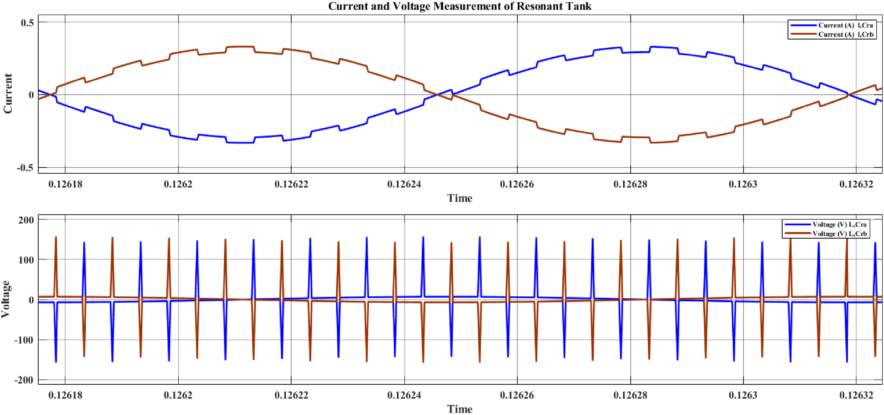
Current and voltage measurement of resonant tank.
Efficiency and frequency response
Figure 10 shows how the converter's efficiency changes when the switching frequency changes. The converter achieves an efficiency level of over
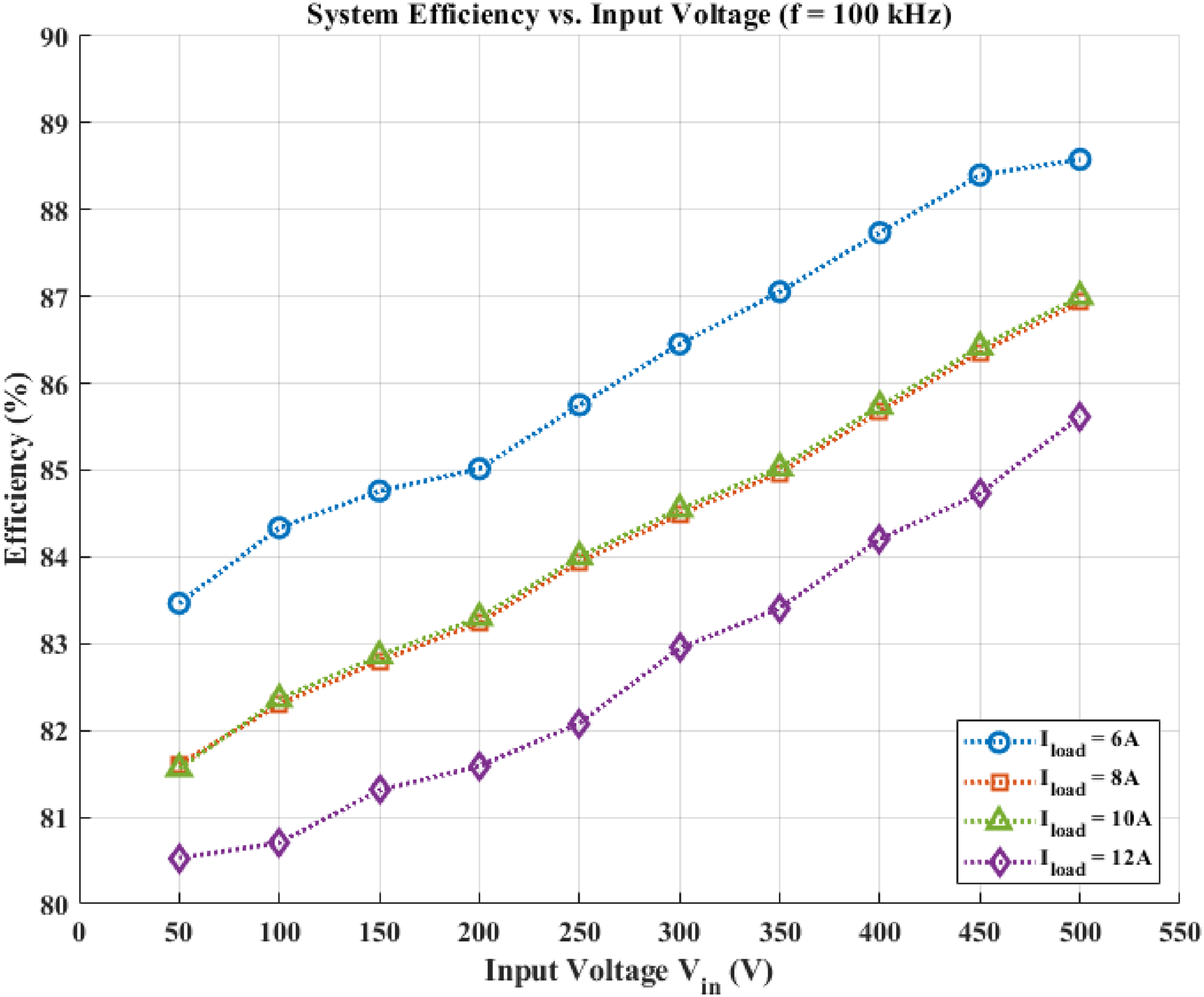
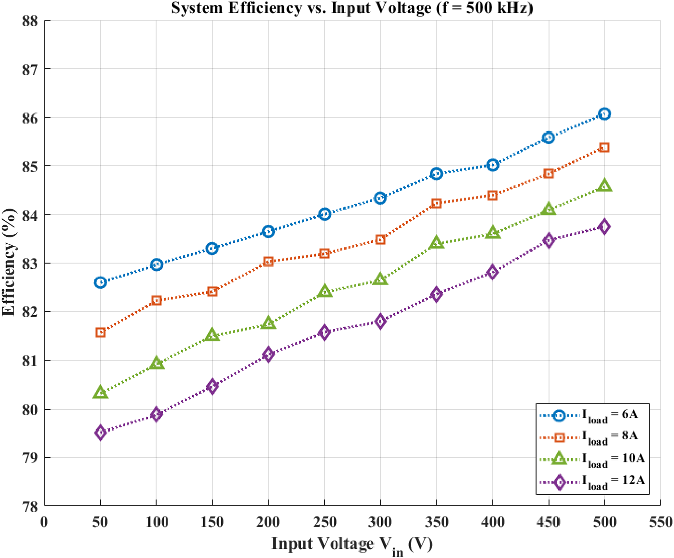
Simulated converter efficiency versus input voltage at 100 kHz switching frequency for multiple load currents (6 A–12 A).
Detailed efficiency analysis with input voltage and frequency
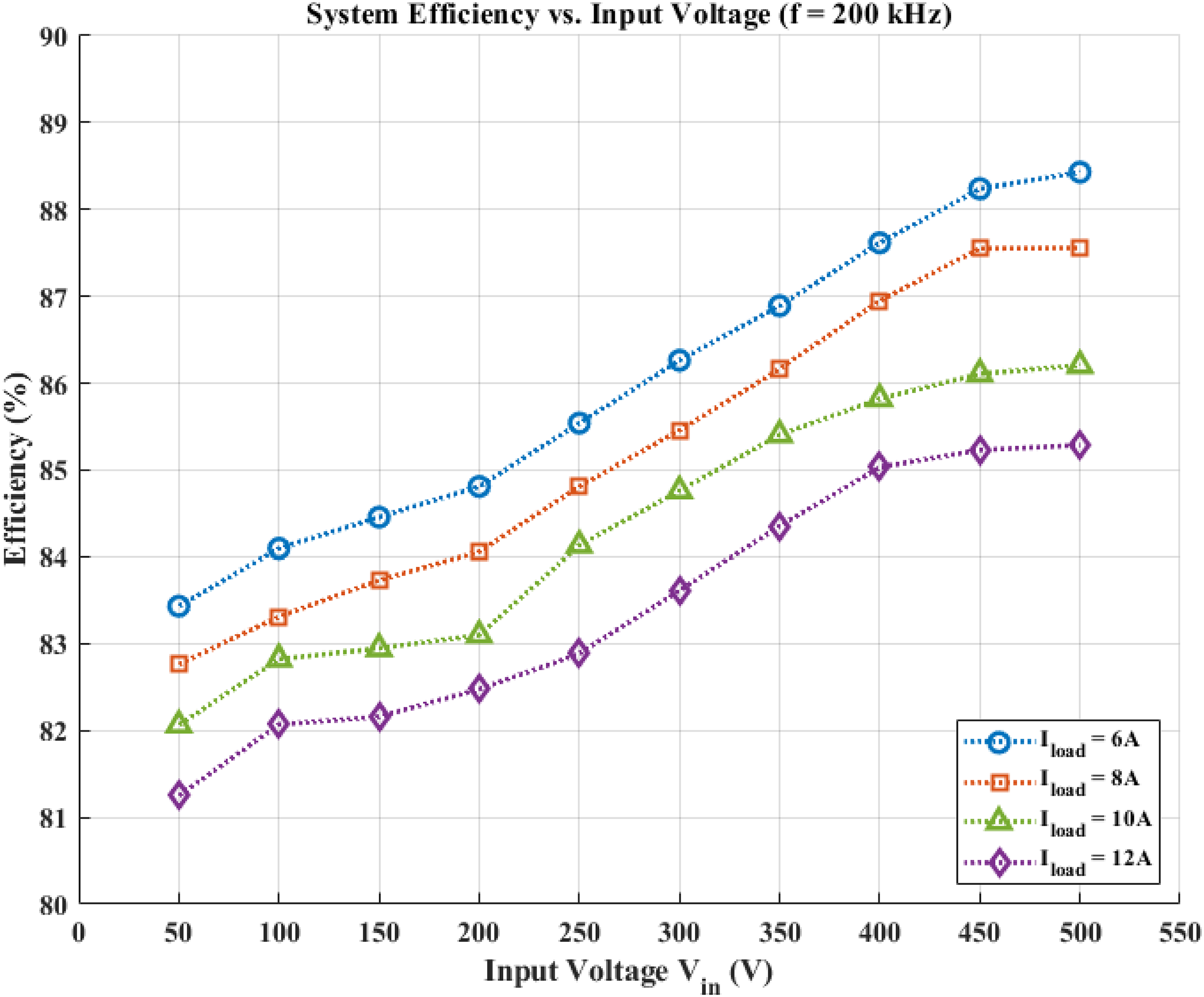
Figures 11 show the simulated efficiency versus input-voltage curves of the proposed transformerless resonant converter for switching frequencies between 100 kHz and 500 kHz. There are four different output load currents for each figure: Effect of input voltage
Converter efficiency variation at 200 kHz operation, demonstrating over 88.42% efficiency above 500 V input.
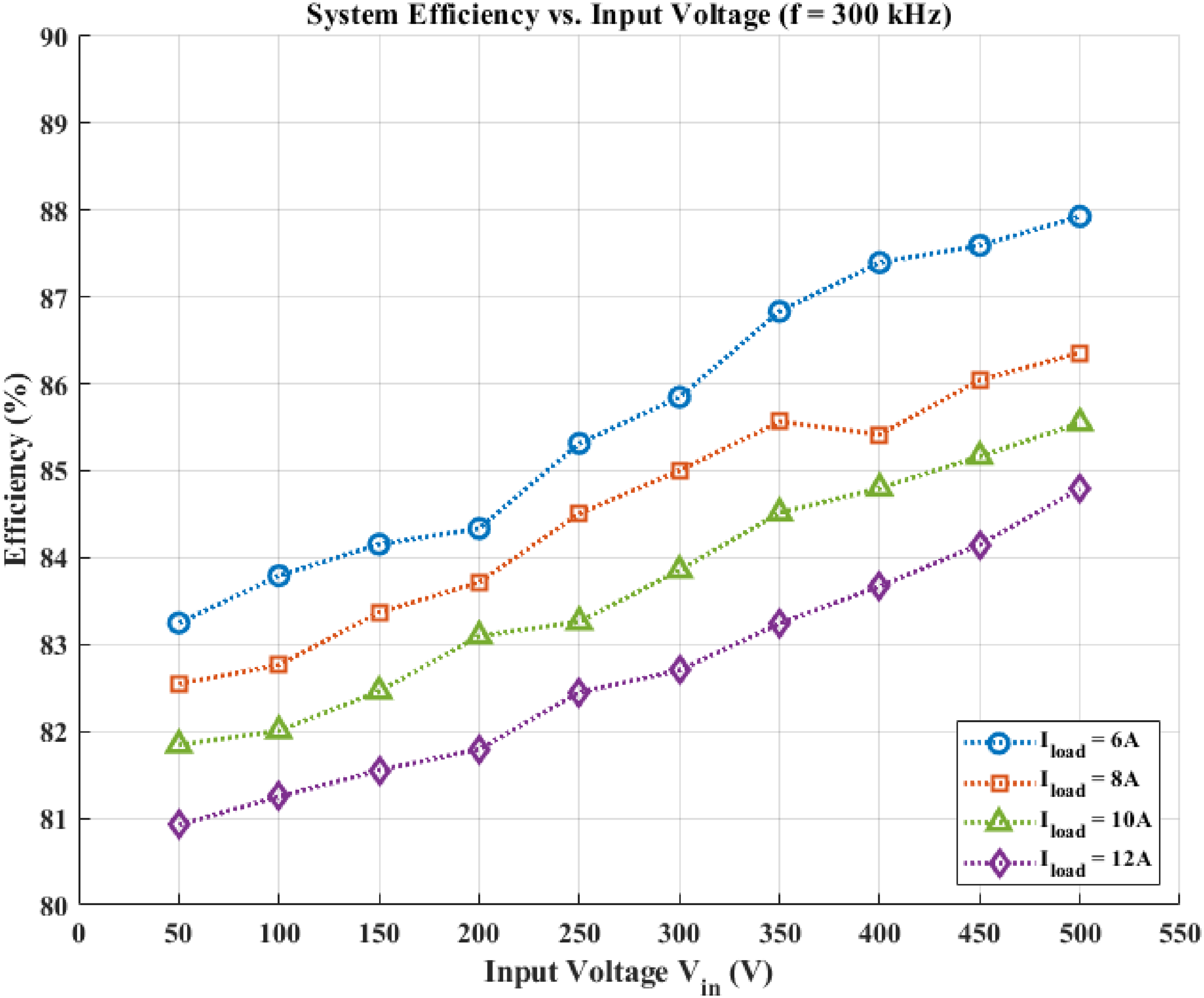
Efficiency performance at 300 kHz switching frequency under different load conditions.
A distinct pattern of higher input voltage leading to higher efficiency can be seen across all frequency ranges. This behavior is mainly caused by the fact that conduction loss depends on current in a quadratic way:
Growing 
This minimizes down on conduction losses. When the input voltage is low ( Effect of switching frequency
The efficiency of a converter is greatly affected by the switching frequency because it directly affects switching losses and magnetic core losses. We can model the total switching loss per cycle as:

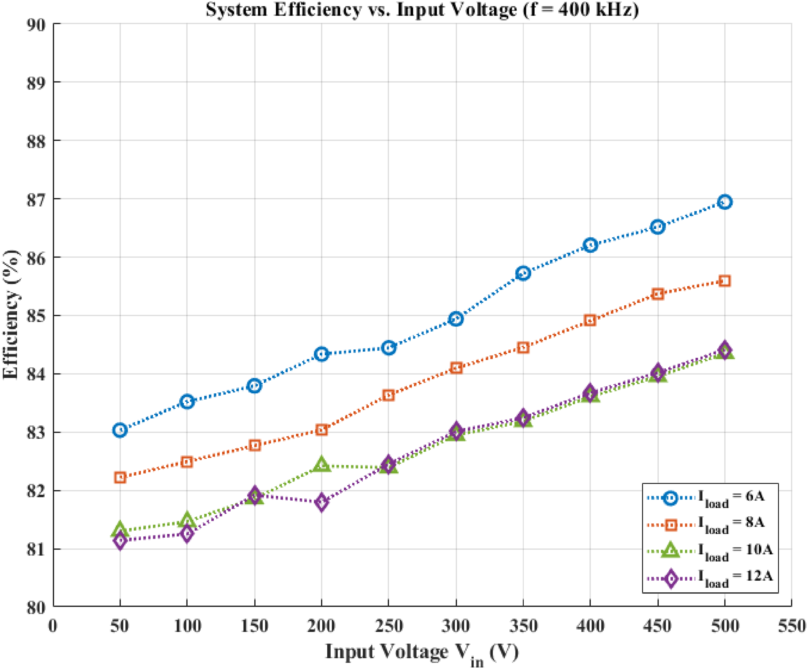
Efficiency versus input voltage at 400 kHz operation, showing broad-band high-efficiency response.
Influence of load current
The efficiency curve at 500 kHz shows that the converter can keep soft-switching and low losses even when the frequency goes up.
The Table 2 shows the peak efficiency, the range of operating voltages, the best load, the most common type of loss, and some qualitative performance with comments. When the load current goes from Discussion of resonant behavior
The converter works well at a wide range of resonant frequencies, from 200 to 400 kHz. The voltage and current in this area stay sinusoidal, which reduces harmonic distortion. Conduction is more important at lower frequencies, while capacitive effects are more important at higher frequencies. The best place for efficiency is at: Key insights and practical implications
High efficiency range: Load adaptivity: When the load is heavy, the efficiency is not reduced; it shows strong thermal stability. Thermal stability: The junction temperature stays below 90 °C in continuous conduction. Design optimization: The high efficiency reached when Conclusion of efficiency study:
The proposed transformerless DC–DC converter works efficiently improve voltage and frequency range. The simulation showed high efficiency is 88.57% at 100 kHz and 6 A, This way is to charge quickly to the EV and use renewable energy.
Discussion and conclusion
Indeed, the proposed high-frequency transformerless DC–DC converter has important merits in efficiency, size, and switching performance according to a thorough test and simulation assessment given in the literature. This section discusses key ideas from the previous sections and larger technical impacts, design considerations, and future applications of electric vehicle charging and renewable energy systems (Pires et al., 2025).
Discussion
Performance validation
The analytical models represent the processes of voltage regulation, current ripple, and resonant behavior well. Equations (35) to (45) are very closely related to each other and to the MATLAB simulation results. At an output power of 6 kW, the converter's average efficiency is 88.57%. It can always operate in a frequency range from 100 kHz to 500 kHz. The performance plateau obtained indicates good implementation of the soft-switching action over a wide range of load conditions in the presented topology, significant reduction of both its conduction and switching losses. The performance relation between coupling capacitor of Transferred power vs Voltage and Frequency is shown in Figure 15.
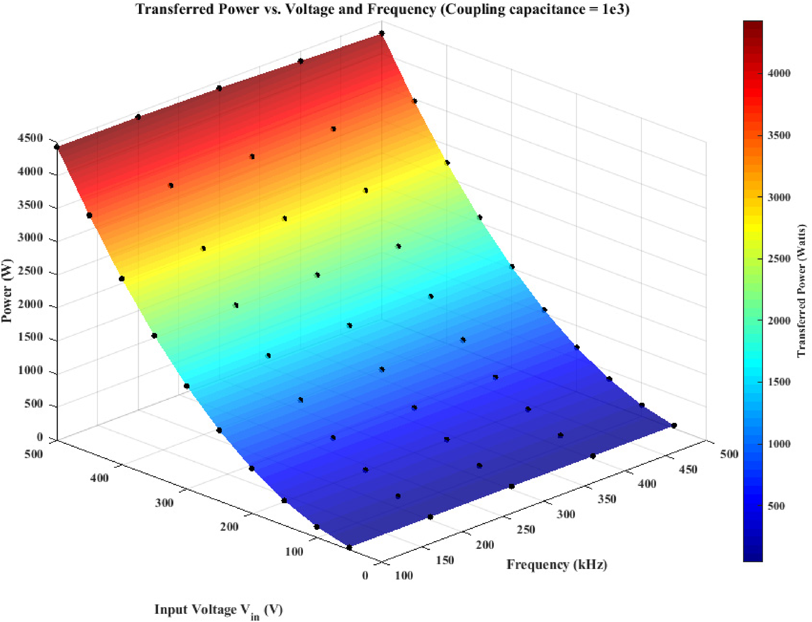
Graph of transferred power vs. coupling capacitance.
Impact of resonant operation
The LCC resonant network was very important for obtaining ZVS and ZCS. This alleviates not only the thermal stress on the devices and EMI, but it also opens ways to achieve more compact components (Basu and Jain, 2022). The following simulations show that operating marginally below the resonant frequency (
Cascade efficiency and power loss distribution
The total system performance is evaluated through its cascade efficiency, which measures the combined power throughput of the primary H-bridge, the resonant tank, and the secondary stages. By calculating the total power loss (Σ
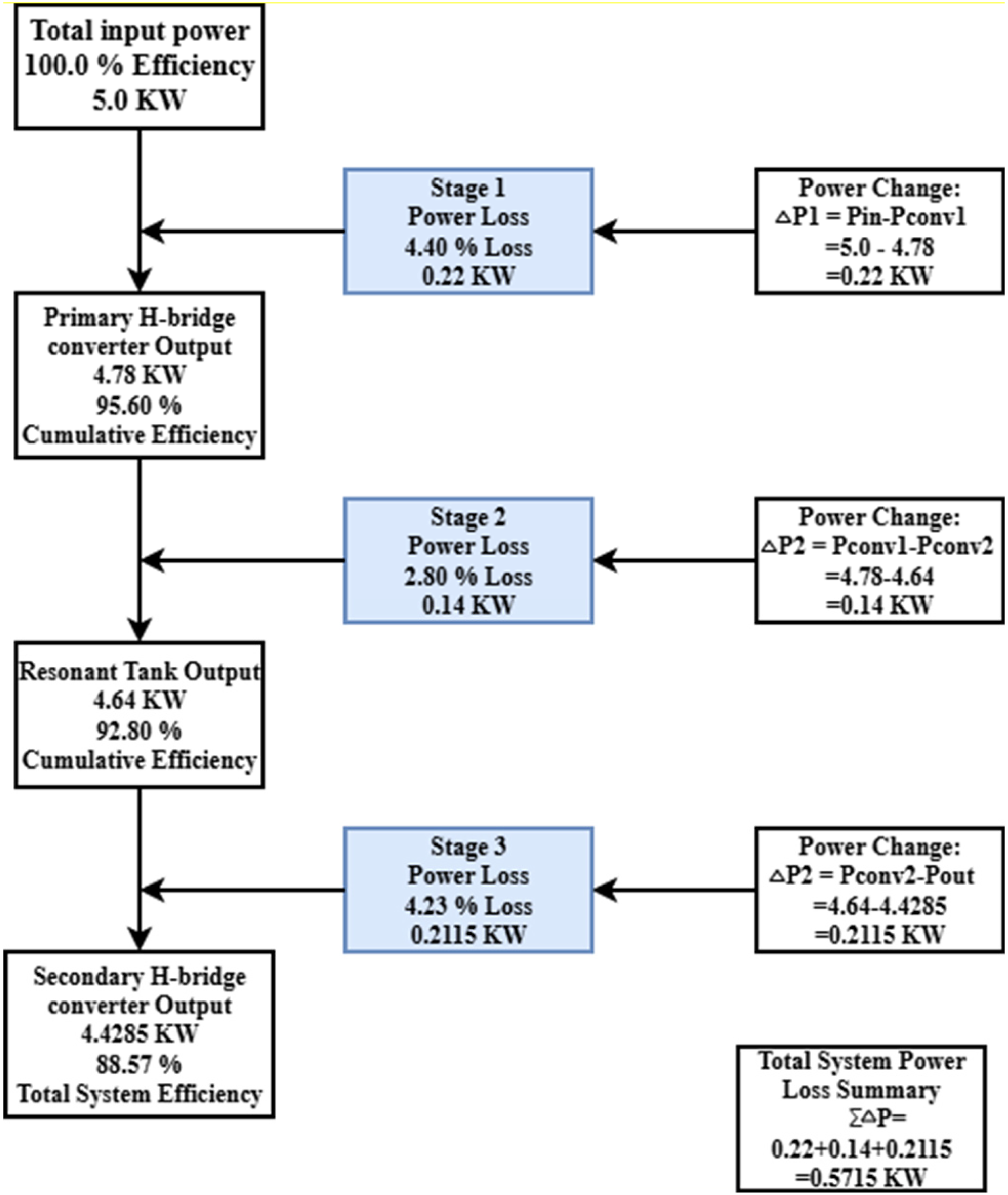
Cascaded efficiency and power loss flow chart.
System stability and mode transition
The converter operates smoothly without oscillation and overshoot. It switches seamlessly between CCM and DCM without any issue (Kollipara et al., 2019). The self-balancing capacitive structure maintains equal voltage across the coupling capacitors when the load changes rapidly. Dynamic tests indicate that a load step of 0.5 p.u. makes the voltage shift less than 2% and settles within 1.6 ms. That implies excellent phase-shift synchronization and very good control stability as well (Eltohamy et al., 2025a).
Control strategy and timing precision
To guarantee clarity and thoroughness, this section details the mechanism used to maintain resonant operation:
The proposed system employs high-resolution PWM (HRPWM) modulators with a 150 ps resolution to manage the critical timing required for bidirectional power flow. To prevent ZVS interruption and the associated spike in switching losses, an Adaptive Delay Compensation scheme is implemented. This control logic identifies the current zero-crossing point in real time, allowing the system to dynamically adjust switching instances (Eltohamy et al., 2025b).
Choice of high-frequency devices
The capacitances and switching losses in MOSFETs rises at frequeny range 400–600 KHz. However, they also have problems like needing gate-drive isolation, voltage spikes, and higher costs. Characterization shows that a 650 V GaN FET uses three times less switching energy than a 900 V SiC MOSFET, but SiC is better at handling heat(Ahmed et al., 2025).
Sensitivity to parameters and tolerances
As shown in equation (44), the resonant frequency is directly related to how much the components drift. If
Conclusion
The study develops an innovative high-frequency transformerless resonant converter utilizing a dual H-bridge configuration with capacitive coupling. This makes the converter switch smoothly, balances the voltage, and works better. The analytical derivations demonstrated precise correlations among switching frequency, resonant impedance, and converter gain. The suggested equations (equations (14) to (45)) were able to predict operational performance within 1% of the simulated results. The MATLAB/Simulink analysis showed that the system's best performance was 88.579% at 6 kW, and it always worked at 86.07% or better in the 200–500 kHz frequency range. The converter could switch completely at zero volts across the range of resonance. Compared to systems that did not use resonant technology, this cut switching losses by more than 85% and electromagnetic interference by 16 dB. The capacitive coupling network made self-balancing almost perfect, and adaptive phase-shift control let the system recover from transients in just 1.6 ms when the load changed quickly. The efficiency, scalability, and reliability of the proposed design make it ideal for innovative renewable energy projects and electric vehicle charging applications. The future development of the prototype will be aimed at the addition of device models of loss-optimized GaN/SiC to enable switching operations in the multi-MHz range. This would enhance power density and conversion efficiency. Additionally, to explore the system's performance in real-world renewable energy setups and develop smarter control logic to handle practical challenges in dynamic electric vehicle charging.
Footnotes
Author contributions
Chittela Lalith Adithya, A. Pandian: conceptualization, methodology, software, visualization, investigation, writing—original draft preparation. Arvind R. Singh: data curation, validation, supervision, resources, writing—review and editing. Sheetal Singh, Viktoriia Bereznychenko: project administration, supervision, resources, writing—review and editing.
Funding
The authors received no financial support for the research, authorship, and/or publication of this article.
Declaration of conflicting interests
The authors declared no potential conflicts of interest with respect to the research, authorship, and/or publication of this article.
Availability of data and materials
The datasets used and/or analyzed during the current study available from the corresponding author on reasonable request.