
Abstract
Fabricating arrays for high-frequency image applications such as ophthalmic imaging, intravascular imaging, and small animal imaging is challenging. For example, an array for intravascular imaging must be small enough to fit within the lumen of a catheter and inexpensive enough to be discarded after a single use. This article presents a new method for fabricating high-frequency annular arrays that is simple and inexpensive. The annular array elements are defined by the electrode pattern on a back surface of a polyimide quarter-wavelength matching layer that is glued to the front face of a ceramic transducer substrate (PZT5H). Electrical losses associated with bonding the matching layer to the transducer substrate are reduced by fabricating a second set of electrodes on the transducer substrate and then bonding the substrates using an anisotropic conductive epoxy. The feasibility of this technique was established by fabricating a seven-element, 20-MHz, 5-mm diameter annular array. The prototype array produced a pulse with a −6-dB factional bandwidth of 50%, an insertion loss of 22 dB, and secondary lobes in the radiation pattern at f/2 that decreased to −65 dB with respect to the main lobe with a peak amplitude of −53 dB.
Keywords
High-frequency ultrasound imaging systems, such as those used for ophthalmic imaging or intravascular imaging, often use single-element transducers. 1 Although these systems could benefit from an array transducer, the cost or complexity of an array has restricted this advancement in many commercial systems. We have developed an easy, inexpensive, and robust method for fabricating high-frequency annular arrays. There are two novel features of our approach. First, a flexible printed circuit board (flex circuit) is bonded to the front face of the transducer. The flex circuit is used to define the annular array pattern and make electrical contact from an external electrical connector to the transducer substrate, and it also functions as a front matching layer. Previous designs that incorporated a flex circuit in the acoustic stack of the array placed the flex circuit adjacent to the back face of the transducer.2-4 To avoid degrading the bandwidth of the transducer, either the flex circuit had to be selected so that it was acoustically thin at the operating frequency, 2 which limited the transducer’s frequency, or the backing material had to be chosen to match the acoustic impedance of the flex circuit, 3 which made the design unsuitable for PZT or single crystal substrates. Both problems are avoided by moving the flex circuit to the front face of the transducer. Second, we use anisotropic conductive epoxy to make electrical and acoustic contact between the traces on the flex circuit and a rectangular grid of electrodes on the surface of the transducer substrate. Previous designs bonded the flex to the transducer substrate either using conductive epoxy, followed by dicing to remove the epoxy between array elements, 2 or using nonconductive epoxy.3,4 Dicing is not possible for an annular array, and although laser micromachining could be used for fabricating an annular array, it is an involved process.5,6 Bonding the flex circuit and transducer substrate using nonconducting epoxy is a viable option for PVDF or copolymer substrates, but it would be problematic for ceramic or single crystal substrates. The dielectric constant of a ceramic or single crystal transducer substrate is so much larger than the dielectric constant of the epoxy that the response of the array elements would be very sensitive to variations in the bond thickness. Furthermore, an unacceptably large voltage drop across the bond layer could result unless the epoxy layer is very thin (< 0.5 µm). The technique we have developed using anisotropic epoxy avoids these problems and provides an easy and low-loss method for connecting the flex electrodes to the transducer substrate. A relatively thick bonding layer (~ 1-2 µm) can be tolerated as the epoxy simply becomes part of the matching layer. Unlike other forms of wire-free bonding, 7 our method does not require special tools to align the transducer substrate and flex circuit during the bonding process, and since the electrodes on the flex circuit and transducer substrates are defined using photolithography, the technique can easily be extended to smaller (< 1 mm diameter) and/or higher frequency (> 20 MHz) annular or linear arrays.
Array Fabrication
Figure 1 shows a cutaway view of the 20-MHz, seven-element, annular array that we fabricated. We discuss the figure starting with the bottom layer, which is the flex circuit that forms the front matching layer and also defines the annular array electrodes. The annular array electrodes and connecting traces are defined by a 2-µm-thick copper layer on the surface of the flex circuit. We designed the array to have seven equal area elements (1.2 mm2) and an outer diameter of 5 mm. The spacing between the array elements ranges from 0.5 mm between the inner and second elements to 50 µm between the sixth and seventh elements. The dimensions of the array were selected using the method outlined by Brown et al. 8 The relatively large spacing between the annular array elements reduces the width of the spatial impulse response of the array and decreases the amplitude of secondary lobes in the radiation pattern at small f-numbers. 8
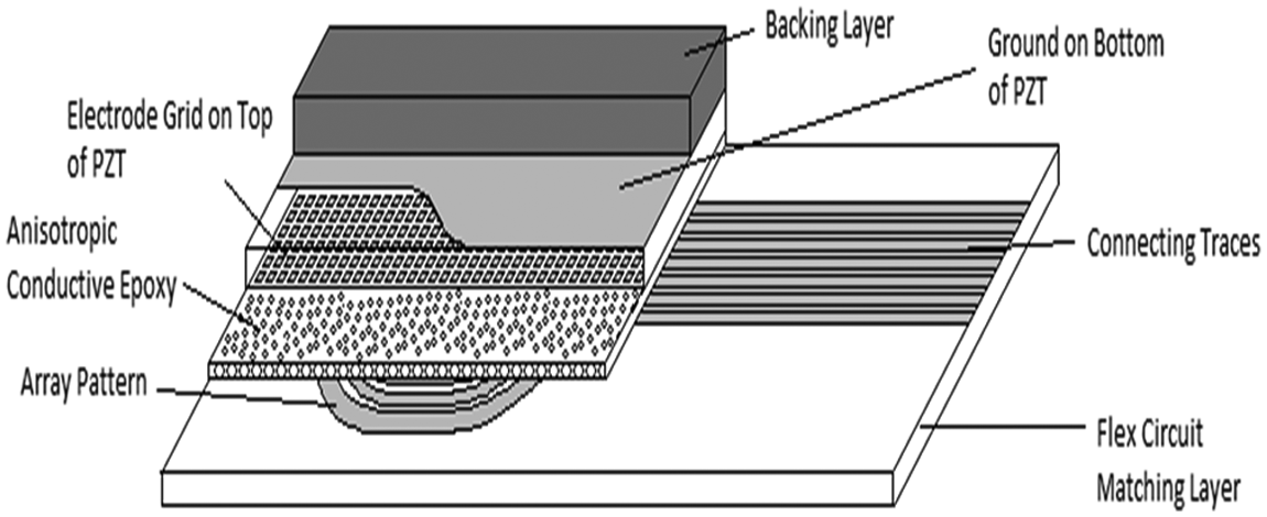
Cutaway diagram showing the layers in the proposed annular array transducer. The front face of the transducer is facing down.
The flex circuit was fabricated by a commercial vendor (Microconnex, Snoqualmie, Washington). The speed of sound, mechanical impedance, and thickness of the polyimide flex circuit substrate were measured to be 2435 m/s, 3.5 MRayls, and 30 to 32 µm, respectively. The thickness of the flex circuit corresponds to one-quarter of the ultrasound wavelength at 20 MHz, which is the designed center frequency for the array. The flex circuit was bonded to the transducer substrate using an anisotropic conductive epoxy (Delo-Monopox AC265; Delo, Windach, Germany) consisting of 1-to 2-µm conducting spheres suspended in an epoxy matrix. During the bonding process, the conducting spheres become trapped between the electrodes on the surface of the flex circuit and electrodes on the mating face of the transducer substrate, and the two substrates become electrically connected. In the direction parallel to the bond layer, the epoxy matrix keeps the spheres from touching, and no conduction occurs. Ideally, the electrode pattern on the surface of the transducer substrate would be the mirror image of the electrode pattern on the flex circuit. However, if this were done, the flex and transducer substrates would need to be carefully aligned during the bonding process to avoid shorting adjacent electrodes. To avoid this problem, we instead used a rectangular grid of electrodes on the transducer substrate. Isolation between adjacent electrodes is maintained by selecting the dimensions of the grid so that the diagonal length of the square electrodes on the surface of the transducer substrate is smaller than the spacing between the annular electrodes on the flex substrate. Here we designed a grid with 30-µm-wide squares with 15-µm gaps. Chabok et al. 9 have previously shown that this technique could be used to bond a flex circuit to a rectangular grid of electrodes on the surface of a 1-3 composite, although in their case, a nonconductive epoxy was used. We have also used a similar technique to bond PZT to silicon substrates. 10 Provided the center-to-center spacing of the grid elements on the transducer substrate is less than one wavelength, it has been shown that little degradation in the radiation pattern will result from the somewhat irregular annular array elements. 10 The grid on the surface of the transducer substrate was formed by evaporating a chrome (5 nm)–gold (50 nm) electrode and patterning the electrode using photolithography. A chrome-gold electrode was also deposited on the back surface of the transducer substrate to form the ground electrode. The transducer substrate was 115-µm-thick PZT5H (TRS200HD; TRS Technologies, State College, Pennsylvania). The final layer in the array is a backing layer of tungsten-loaded epoxy (EPOFIX; Electron Microscopy Sciences, Hatfield, Pennsylvania) mixed 6:1 (epoxy:tungsten) by weight to give an acoustic impedance of 10 MRayls. 11
The transducer was assembled by first securing the flex substrate to a glass lapping plate using masking tape (Henkel Consumer Adhesives, Inc., Mentor, Ohio). A drop of anisotropic conductive epoxy (Delo-Monopox AC265; Delo) was applied to the exposed copper rings on the flex substrate, and the ceramic was placed grid side down on the flex substrate. The entire assembly was then clamped using a spring-loaded bonding jig (model BJ2; Logitech, Glasgow, Scotland). A 1.5-mm-thick layer of polypropylene was placed between the plunger and the transducer to act as a pressure distribution layer, and aluminum foil was used to prevent excess adhesive from sticking to the clamp. The clamp was applied using light pressure (approximately 10 kg/cm2) from a spring and a single turn of a screw clamp. The assembly was then placed into an oven and heated to 180°C for five minutes, after which it was removed and allowed to cool. Figure 2 shows a photograph of the front face of the transducer just after release from the bonding jig. The electrode grid on the transducer substrate can be seen though the flex substrate in the spaces between the annular array electrodes. This is the view that would be obtained in Figure 1 by looking up from the bottom of the figure. Contact between the ground electrode on the ceramic (second layer from top in Figure 1) and the grounded connecting trace on the flex cable was made using a thin wire and conductive epoxy (E-Solder No. 3022; Von Roll USA, Inc., New Haven, Connecticut). To complete the transducer, a stainless steel casing was tacked down to the ceramic using conductive epoxy, and the casing was then filled with tungsten-loaded epoxy. Finally, a backplane connector (DF12; Hirose Corporation, Tokyo, Japan) was soldered to the pads on the flex circuit. To verify connectivity, we made impedance measurements of the array elements using an impedance analyzer (model 4396B; Hewlett Packard, Palo Alto, California). The results of these measurements are shown in Figure 3. The array had equal area elements, so the impedance should be same for all the array elements. However, the effective area of the outer elements was slightly larger due to mechanical coupling, and consequently, the magnitude of the impedance decreased slightly from the central element (element 1) to the outermost element (element 7). This effect has previously been reported by Brown et al. 8 The dual peaks in the impedance magnitude plot are characteristic of transducers employing a single matching layer and result from the coupled resonances in the matching layer and transducer substrate. For comparison, Figure 4 shows the theoretical impedance magnitude (KLM model) for a single element of the array. The mechanical impedance of the flex and the area of the array elements used in the model were adjusted by trial and error to account for the mass loading of the copper and the decrease in active area introduced by the electrode pattern on the PZT, respectively. Reasonable agreement between the theory and experiment was obtained using an element area of 1.1 × 10⁻⁶ m2 (a decrease of 10% from the designed value) and flex impedance of 5.2 MRayls. The upwards swing in the impedance magnitude between 40 and 50 MHz results from the transmission line effect introduced by the connecting traces on the flex.
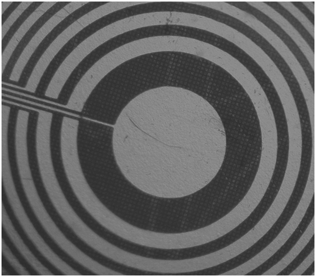
Microscope image of the front face of the transducer just after the flex circuit was bonded to the PZT. The rectangular grid of electrodes on the surface of the PZT can be seen through the spaces between the electrodes on the flex. Electrical contacts to the array elements can be seen on the top left side of the image. The diameter of the inner electrode is ~ 1.2 mm.
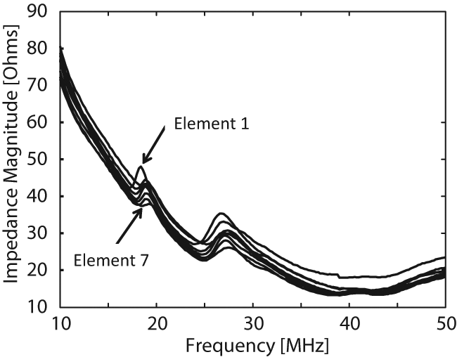
Experimental impedance magnitude measurements for the completed array.
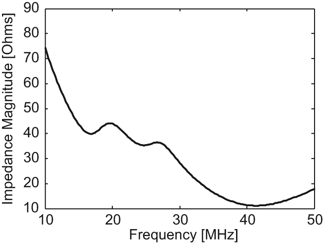
Theoretical impedance magnitude for a single array element.
Results
Figure 5 shows the pulse-echo response of the central element of the array and the corresponding magnitude spectrum. The pulse-echo response was measured in a water tank by recording the reflection from a quartz flat placed 10 mm in front of the transducer. The transducer was excited using a mono-cycle pulse (30 Vpp), and the detected signal was recorded using the 50-Ω input to a digital oscilloscope. The transducer was connected to the oscilloscope using a protection circuit consisting of a λ/4 cable (at 22 MHz) terminated at the oscilloscope by a limiter. The pulse spectrum was calculated in software. The pulse had a center frequency of 22 MHz and a −6-dB fractional bandwidth of approximately 50%. For comparison, a KLM model was used to calculate the pulse-echo response and pulse spectrum of the transducer. There is good agreement between the experiment (Figure 5) and the KLM model calculation (Figure 6).
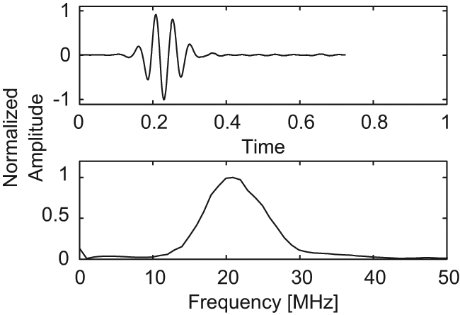
Experimental pulse-echo response (top) and spectrum (bottom) for the central element.
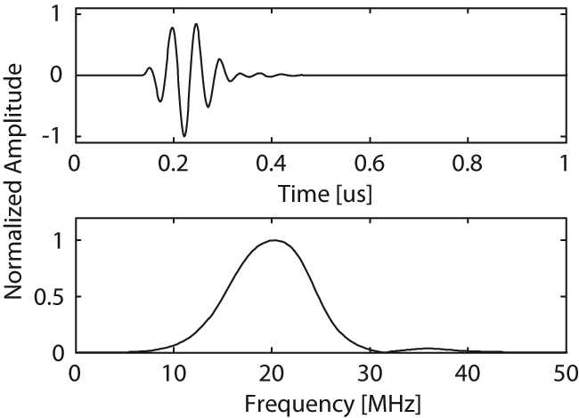
Theoretical pulse-echo response (top) and spectrum (bottom) for the central element.
The insertion loss for the central element of the array was measured by placing a quartz flat in a water bath 5 mm from the face of the array and measuring the pulse-echo response and also the excitation pulse using the 50-Ω input of a digital oscilloscope. The insertion loss was calculated from the ratio of the magnitude spectrums of the pulse-echo response and excitation pulse. Corrections were made for the reflection coefficient of the quartz flat as well as the attenuation of the water, but diffraction losses were ignored. This resulting insertion loss is shown in Figure 7. A minimum insertion loss of −22 dB was obtained at 24 MHz.
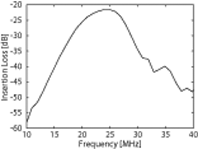
Insertion loss for the central element. The measurement was made by recording the signal reflected from a quartz flat placed at a depth of 5 mm in a water bath.
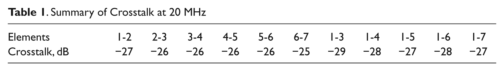
The crosstalk between adjacent elements in the array was measured in a water bath by exciting one element with a 4-Vpp, 20-MHz sinusoid and recording the signal on a second element. The results are summarized in Table 1. The crosstalk between adjacent elements was approximately constant with an average value of −26 dB. The crosstalk between the central element and elements 2 to 7 was also relatively constant, ranging from −27 dB to −29 dB. This is slightly better than the −20-dB level reported by Brown et al. 8 for a kerfless PZT annular array but much worse than the −37-dB to −50-dB levels reported by Chabok et al. 9 for a 1-3 composite annular array. It should be noted that since annular arrays do not steer the beam away from the axis of the transducer, relatively high crosstalk (~ −20 dB) can be tolerated with little degradation of either the radiation pattern or the pulse shape. 12 The resistance between adjacent array elements was also measured at DC using an ohmmeter and was found to be greater than 10 MΩ.
Summary of Crosstalk at 20 MHz
The two-way radiation pattern of the array was measured in a water bath by scanning the array across a point target placed in front of the transducer. The point target was fabricated by drawing out a heated glass rod to produce a fiber with a thickness of approximately 125 µm and then melting the tip of the fiber to produce a spherical knob (~ 200 µm diameter). This was mounted vertically in a water tank with the stem of the glass target along the axis of the beam and the tip 10 mm from the transducer face. The array was focused to a depth of 10 mm (f/2) using an in-house transmit beamformer with delays produced using DS1023 digital delay chips (Maxim, Sunnyvale, California). The transducer outputs were connected to the oscilloscope using a λ/4 (at 22 MHz) coaxial cable terminated by a limiter. The output of the limiter was connected to a 115-MHz low-pass filter (SBLP-117; Mini-Circuits, Brooklyn, New York) and a 35-dB amplifier (model AU-1466-9014; MITEQ, Hauppage, New York) before terminating at the 50-Ω input to the oscilloscope. The response from each element of the array was recorded individually and exported to MATLAB (MathWorks, Inc., Natick, Massachusetts) for beamforming. The array was then scanned laterally across the point target and the process repeated at each step in the scan. The resulting two-way radiation pattern at f/2 is shown in Figure 8. The radiation pattern has a −6-dB main lobe width of 160 µm, which corresponds to 2.1 wavelengths at 20 MHz. A peak secondary lobe amplitude of −53 dB with respect to the main lobe was found.
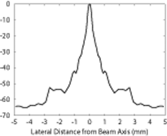
Beamformed two-way radiation pattern of the seven-element annular array at f/2.
Discussion and Conclusions
A relatively simple and inexpensive method for fabricating high-frequency annular arrays has been developed. The cost of the PZT, flex, and expendable materials associated with the fabrication of the array was on the order of a few hundred U.S. dollars when averaged over the construction of 10 arrays. The method uses a flexible printed circuit board to define the annular array elements and to make the connections from the array elements to an external connector. By choosing an appropriate thickness for the flexible printed circuit board, it can also be used as a quarter-wavelength matching layer. The fabrication process is simplified by defining a grid of square electrodes on the transducer substrate with the size of the square electrodes chosen to be smaller than the separation between the annular array electrodes. Since it is impossible for an electrode on the transducer substrate to bridge the gap between the electrodes on the flex, the two substrates can be bonded together using an anisotropic conducting epoxy without having to worry about alignment. The anisotropic epoxy is easy to use, and the connections that are made to the annular array elements during the lamination process are quite robust compared to techniques where individual wires are bonded to the array elements. An additional advantage of this design is that the mechanical impedance of the anisotropic epoxy is very similar to the polyimide flex matching layer, so the pulse shape is not degraded by the presence of the bond layer.
A seven-element, 5-mm diameter, 20-MHz annular array was fabricated using this method. The array produced a pulse with a −6-dB bandwidth of 50%. The beamformed two-way radiation pattern showed a strongly focused main beam with a −6-dB beam width of 2.1 λ at f/2 and a pedestal secondary lobe that was suppressed by approximately 60 dB with respect to the main lobe with a peak of −53 dB. Although we describe the fabrication of a 20-MHz annular array, the method could easily be used to fabricate smaller higher frequency arrays. The minimum standard polyimide thickness that is commercially available is 7.6 µm, which would correspond to a center frequency of approximately 80 MHz.
Footnotes
Declaration of Conflicting Interests
The authors declared no potential conflicts of interest with respect to the research, authorship, and/or publication of this article.
Funding
This paper was funded; courtesy of National Research Council grant number 216924-2009.