
Abstract
The article has provided a novel way of finding the probability of fracture (Pf) based on modifications of some established concepts. It has also discussed ductile to brittle as well as brittle to ductile transitions in the same coating/substrate system subject to differences in crystallisation, indenter sharpness, sliding modes and dislocation kinetics. The indentation positioning and nanocrystalline features cause ambiguity in the results and need meticulous analysis. As a result of increased dislocation movement, the crystalline portions toughened in contrast to the amorphous parts, which were more brittle. The Pf, which varies and reaches a maximum of 52% in the amorphous or near-amorphous area, was calculated using the Weibull distribution. Transitions between ductility and brittleness can be seen in sliding indentations. Evidence of adhesive failure, which required better coating component inspection because it happened significantly earlier, was shown. Finite-element modelling was used to analyse the stress and provide information on dislocation motions and the impact of indenter shape on fracture. The outcomes are advantageous for the production of devices based on nano/micro-electro-mechanical systems.
Introduction
Hard coatings are mainly made up of transition metal carbides, nitrides, and (oxy)nitrides along with some groups III and IV elements. They exist either as single compounds such as TiN, TiC, SiC, Al2O3, Si3N4, CN x , cBN, diamond (sp3 carbon), etc., or as nanocomposites such as Si–C–N, Ti–Al–N, Ti–B–Si–C–N, etc., which consist of a mixture of different possible phases the elements can make. The individual phases are valence crystals where the neighbouring atoms share their valence electrons under the formation of strong homopolar or covalent bonds. These crystals naturally possess high hardness and are good electrical and thermal insulators.1–3 Diamond is the hardest and talc is the softest material known to mankind. These hard coatings with their various combination of phases have major surface engineering applications in terms of possessing resistance to wear and abrasion properties as well as being corrosion resistant and sustainable to harsh operating conditions, Novel inclusion of elements such as V, Nb, Y, and even some rare earth metals such as Eu have been tried to obtain phases sufficing any technical requirement. 4 Theoretical studies are also being done in parallel with the search for harder and tougher coatings. 5 Several factors start from structural aspects (crystallisation, type and nature of phases formed and their distribution, and interfacial growth), film thickness (causing stress variations) to the nature of force applied (which involves the geometry of the indenter and the mode: static/sliding). These factors are, however, interrelated and influence one another. The fracture nature is also influenced by the interaction of different cracking events.
The depth-sensing nanoindentation and scratch tests have been effective techniques for quite some time now to determine the mechanical properties (including fracture) of the hard coatings as they have minimal influence from the substrate. Due to their high precision, the changes occurring in the crystallinity brought in by compositional or in effect the depositional parameters, get captured with clarity. The fractographical features of the sample surface which have been subject to loading either in static or sliding modes are also related to the compositional alterations. Bringing phase changes is an ambiguous but quite intriguing area of study. The stress at the contact point of the indenter is represented by a combination of the Boussinesq shear stress, due to indenter loading, and Blister stress fields due to residual stress pre-existent in the film/substrate system. 6 These residual stresses are the result of the film composition, surface morphology, and thickness and hence are related to the adhesive, abrasive, wear, and fracture properties of the film. The incorporation of nitrogen in SiC has been reported to improve the toughness. of the resultant Si–C–N film. However, it can also be detrimental at the same time as it promotes graphitisation. The alteration of deposition parameters on the other hand during the film growth significantly changes the composition and the mechanical configuration of the film which includes adhesion properties as well.
As per the standard Hall–Petch effect, a reduction in crystallite size causes an increase in mechanical strength. There are, however, factors that might cause an altered manifestation of this effect viz. having near-amorphous/nanocrystallites that may cause a reduction in mechanical strength. An increase in film thickness which initially tallies with increased crystallisation and grain growth providing good mechanical properties becomes a negating factor after increasing to a certain level due to high tensile stresses getting generated increasing the fragility of the films. 7 All these factors make sliding indentation tests an ambiguous but quite an intriguing area of study especially in the case of nanocomposite coatings.
The positioning of the indentation can reveal significant information about the surface features of the sample under consideration as an in-homogenous crystallisation on the other hand makes the positioning of the indentation(nano) test a deciding factor as well. An alteration in the load–depth plots takes place based on the morphological region of the sample. The tip–sample interactions for indentations performed on the grain, grain boundary, or triple junctions get reflected in the P–h plots which if analysed can get us useful information that shall be helpful, particularly for those materials that rely on surface-based mechanisms such as conduction. adhesion, wear, abrasion, etc. 8 Although the primary phases recognised as hard phases have no electrical conductivity whatsoever, electron flow and even piezoelectricity have been found in certain polymer-derived ceramic-based nanocomposites such as Si–C–N, which have extended their application in making sensors and nano/micro-electro-mechanical systems (N/MEMS). 9
The stress at the interface of a coating–substrate system shows variations in its intensity and nature (compressive/tensile) based on the coating thickness, and coating/substrate material and is even gets influenced by the indentation process. The stress variations can impact the fracture morphology as well as the interfacial fracture energy, depending on the indenter shape, the nature of the substrate, crystallographic properties, pre-existing flaws, internal micro-cracks, or pre-strain. Depending on the prevailing kind of stress, the stress distribution beneath the depression may result in dislocation pile-up leading to strain hardening or crack formation.6,10
The electrical conduction has also been reported to be dependent on the tip–sample contact up to penetration devouring any substrate effect in the case of thin films. The microcrack being generated on the surface and underneath during penetration requires a proper analysis based on zero-point corrections due to tip defects. Materials used in microelectronic fabrication such as Si–C–N require robust as well as conduction-sensitive features and are analysed based on the above-mentioned ways will find proper means of their applicability. The product may be tuned to make it more conducive to the operating conditions when it is used in a device. 9
Considering all these aspects, an attempt has therefore been made in this communication to analyse and assess the fracture from the results of nanoindentation and scratch test on the hard coatings based on microstructural features and correlate the transitions taking place between ductile and brittle failure modes at the different stages of the loading and try to understand the mechanical responses shown by the various crystalline topographical conditions formed in the growth process by deposition. The communication provides a technological perspective that envisages further activity towards the requirements of hard coatings being utilised as protection for mechanical parts subject to harsh operational and environmental conditions as well as miniature devices used in modern-day technologies.
Materials and methods
Ti–B–Si–C–N-based films, which also include TiB2, SiCN, Ti–B–Si–C, and Ti–B–Si–C–N coatings, were deposited on silicon substrates by magnetron sputtering using a sintered ceramic target of SiC and/or TiB2 and a supply of argon and nitrogen gas. The reason for choosing magnetron sputtering as the means of deposition was due to its versatility in the type of materials that can be deposited and stoichiometric control over the deposition.
It is used to deposit a variety of technologically significant coatings for the manufacturing of microelectronic devices, metallurgical protective coatings for tools and aerospace, and even medical science in various surgical equipment. The technique involves the ejection of atoms (called adatoms) from the targets by colliding them with neutral energetic ions (mainly Ar+), which involves momentum transfer and the collision cascade. It is also considered to be a clean process and takes place in a high vacuum. A recent study with a proposed model on sputtering based on different processing parameters has been reported. 11
The target was put in a chamber and evacuated by a diffusion pump using Silicone oil up to a pressure of 10−6 Torr. The depositions were carried out by changing the substrate temperature, power, and pressure (Ar–N2) as reported previously.12,13 The transmission electron microscope (TEM) by Phillips (EM200) at 200 kV was used to study the crystallographic growth patterns in the film. The surface profiles of the images were obtained by ImageJ software. The sliding indentations were performed by Scratch Tester (Ducom, Bangalore) using a Rockwell C indenter. The nanoindentation was performed by MTS Nano indenter, USA using a Berkovich tip.14,15
ABAQUS (Hibbitt K.S Inc., ABAQUS 2002, Pawtucket, RI) was used to do the finite-element modelling (FEM) simulations to examine the stress distribution during the indentation that results in delamination and fracture. In this work, the model is simulated in axis-symmetric 2D conditions because of the specimen's and the indenter's axial symmetry. An axis-symmetric discrete stiff element with a half-included tip angle of 70.3° is used to perform the nanoindentation. Four nodes of axisymmetric CAX4R components represented the substrate and thin film materials. For the model, a total of 68,764 elements were employed, each measuring 150 × 150 nm on each side. This was necessary since the prediction of correct simulation results requires the finer mesh size of the element used for analysis.6,10
Results and discussions
Deviation in P–h plots
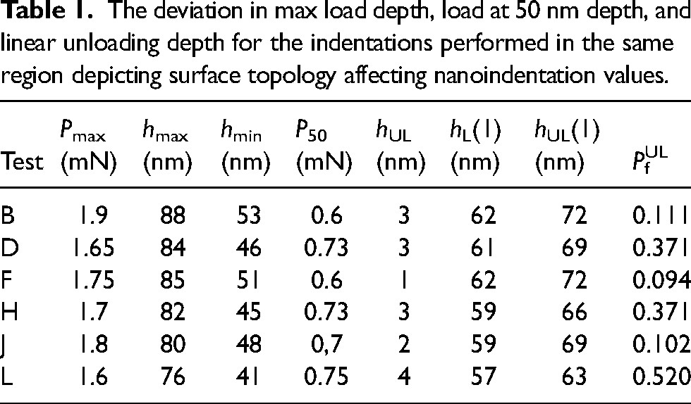
Indentation load scattering and different load-depth curves were reported for indentation at different crystallographic regions of SiCN coatings. 16 The scattering was due to non-uniform stress and varied strength of different types of defects. The load at the grain centre causes the crack to initiate at the grain boundary and junction areas. The quantification of the scattering can therefore be used to determine the stress on the thin films. The P–h plots for indentations performed at different locations on the same sample are shown in Figure 1(a). The TEM image showing the heterogeneous crystallisation which was responsible for the deviations in P–h plots is given in Figure 1(b). It can be observed that although the initial parameters were the same for all the tests, variations are observed in terms of loading and unloading slopes, maximum load required to attain a target depth or vice versa (Pmax, hmax), residual depth (hres or hmin), and linear unloading (hUL) at the end. A tabular representation of the parameters obtained from the tests performed (Figure 1(d) to (f)) is given in Table 1. The exact positions of the tests performed (B, D, F, J, and L) are schematically represented in Figure 1(g).
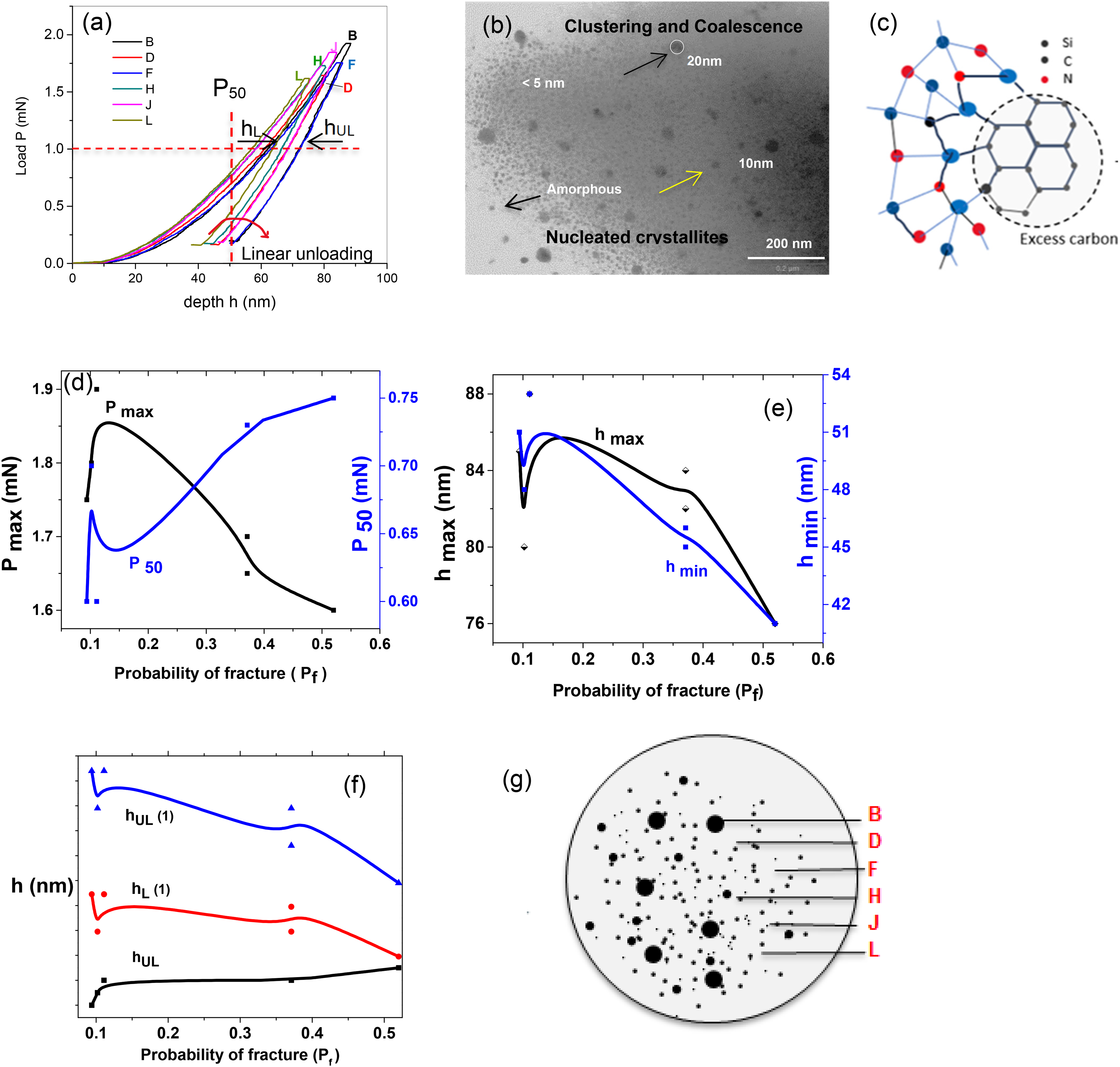
(a) The variations in load-depth (P–h) curves on nanoindentation on Si–C–N hard coatings. 16 (b) The structure of Si–C–N with excess carbon. 19 (c) Transmission electron microscope (TEM) image of the formation of nanocrystallites during the sputter deposition process, which has clustered and coalesced to form bigger crystallites. 13 (d) The variation of probability of fracture (Pf) obtained by modification of Weibull distribution with max load applied (Pmax) and load applied or penetrating 50 nm depth (P50). (e) Maximum and minimum (residua) depth. (f) Linear unloading and penetration depth at 1 mN load for both loading (hL(1)) and unloading (hUL(1)) stages. (g) Schema of different crystallographic oriented regions where nanoindentations were performed.
The deviation in max load depth, load at 50 nm depth, and linear unloading depth for the indentations performed in the same region depicting surface topology affecting nanoindentation values.
A parameter called P50, that is, the load at 50 nm depth for all the cases was measured and tabulated to correlate the different tests. The penetration depths for both loading and unloading at 1 mN load represented as hL(1) and hUL(1) were also taken into consideration. A higher penetration depth (load) causes dislocation-based creep. An opposite effect, however, takes place on increasing the strain rate. 17 The strain rate is kept fixed at 0.05 s−1, a non-conservative dislocation climb has therefore been active in regions of crystallisation causing the deviations in P–h plots. An analogy can be also drawn with ductile to brittle transitions (DBTs) taking place during nanoindentation as crystalline to amorphous phase transitions have been prevalent in metal–organic frameworks, 18 which is like the Si–C–N structure with some excess carbon 19 (Figure 1(c)).
Ultrafine crystallisation
The formation of nanocrystallites can be seen in the TEM image given in Figure 1(b). Ultrafine crystallites even <5 nm or just above the amorphous state can be seen to form which eventually after clustering and to some extent coalescence give rise to nanocrystallites of size ∼20 nm. The Hall–Petch relation which predicts an increase in strength with a decrease in nanocrystallites size should therefore hold in this case and growth. However, in the adjacent near-amorphous regions, the Inverse Hall–Petch relation is expected to hold causing a decrease in strength. The position of the indentation is therefore crucial as the mechanical response depends upon the extent of nucleation which might have occurred in the area. The deposition parameters as previously reported have a strong influence on the extent of nucleation or growth of the crystallites. 13 Although visual inspection of the TEM image can be interpreted to understand the crystalline nature of the sample, as can be seen in Figure 2(a), where nanocrystallites of about 20 nm can be seen to have grown, selected area electron diffraction (SAED) patterns provide the full confirmation about the sample being crystalline, amorphous or near amorphous. The SAED pattern corresponding to near amorphous or nanocrystalline growth mainly consists of low-intensity concentric rings as can be seen in Figure 2(b), which has been inverted in greyscale and enhanced in sharpness and contrast for clarity.
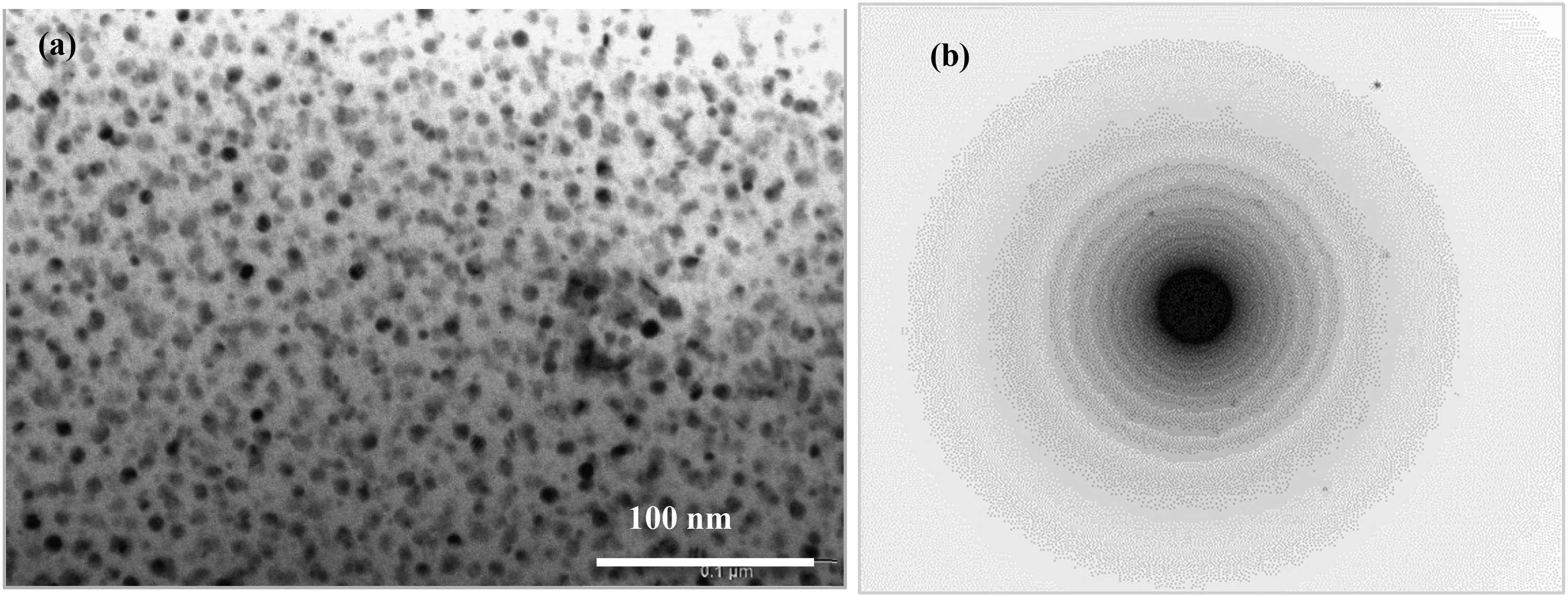
(a) A TEM image of magnetron sputtered Si–C–N coatings showing the formation of nanocrystallites and (b) its SAED pattern representing near amorphous (nanocrystalline) growth.
Due to this nanoscale ultrafine crystallisation, the indenter tip comes in contact with the film surface with varied morphologies and therefore results in minor differences in the P–h plots. 8 The variations in this case are, however, much more subtle due to the much-decreased distribution of the morphological variations. The tip-bluntness also has a role to play in this case as sharper tips cause more plastic deformation and result in fewer deviations whereas samples under blunt tips with nearly Hertzian contact are more prone to surface fractures. Tip calibrations are therefore performed after a certain period of use. The elastic inhomogeneity occurring in a nanocomposite system, which is a conjunction between embedded phases in a matrix, has been addressed recently. 20
The indentations were performed in amorphous, near amorphous as well as regions that underwent different levels of crystallisation. For the tests having the lowest Pmax (1. 6 mN), that is, test L, the loading portion was found to have the highest slope (or P50 = 0.75 mN), which means a higher resistance offered to the indenting. The unloading depth and the probability of fracture (Pf) were found to be highest for test L. All these observations indicate a brittle behaviour and point to the fact that the indentation has been done on the amorphous or near-amorphous regions.
The Pmax values were lowest for test F which also showed the lowest slope and P50 value (0.6 mN) indicating comparatively the highest toughness to be prevalent in this case. The position of indentation in this case is on the coalesced crystallites of about 10 nm size as seen in the TEM image. Tests B and J also showed lower Pf values (0.111 and 0.102) and were done on similar coalesced crystallisation regions with larger sizes (∼20 nm). The Hall–Petch (σy ∼ 1/d 0.5) effect with mechanical strength (yield stress, σy) inversely proportional to the crystallite size (grain size, d) seems to be persisting in this case. An increase in the Pf was observed for tests D and H showing the same Pf values of (0.371) as well as P50 values of 0.73 mN. The indentation region of these tests was on the region where the nucleation of the crystallites had just initiated and their sizes were <5 nm. The mechanism of the inverse Hall–Petch effect in these regions caused a lowering of the mechanical strength. The reason is that having no specific slip system due to lack of crystallinity, the near-amorphous regions are more probable to a brittle failure.
The formation of small crystals may cause an increase in hardness due to enhanced dislocation motion which includes dislocation climbs giving rise to strain hardening, but strictly speaking, may or may not lead to an increase in fracture toughness in the same way. 1 Although there is evidence of phenomena such as crack deflection to account for an increase in toughness, for those positions that offer an initial high resistance to penetration, the chances of fracture increase as the initial high stress imposed by the indenter gets arrested in the material showing no signs of fracture initially until the applied stress imposed by the indenter exceeds the fracture toughness (KC) threshold value.
Fracture probability
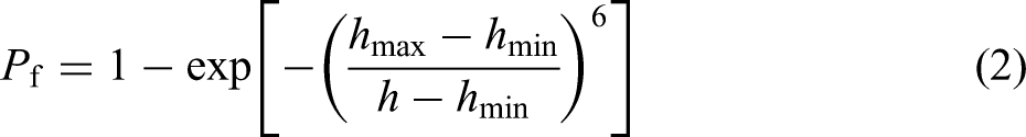
The fracture behaviour of hard ceramic coatings is mostly brittle. However, using a sharp indenter at the nanoscale may reveal a feeble ductility before DBTs in the fracture process in both static and sliding (scratch) modes. This fracture behavior is a critical and complex phenomenon and is crucial in material selection and design applicable to aerospace engineering, fabrication of microelectronic device components, bioceramics used for bone implants, etc. To establish a relationship that quantifies this critical failure behaviour in the DBT region, the two most accepted and recommended standard methods are the Charpy impact test and the master curve methodology. Due to the drawbacks of Charpy impact tests such as not providing fracture toughness by itself, giving only the lower bound of the fracture toughness values, and incapability in arresting the statistical scatter of the fracture toughness values, the master curve methodology is the preferred one to be used. It is based on modeling cleavage fracture in the transition with a three-parameter Weibull distribution. The Pf can be expressed as given in equation (1)
21
:
For ductile failure, as the film thickness increases, the fracture toughness also increases but is followed by a decrease due to the transition from plane stress to plain strain condition, until a plateau is reached, after which the toughness remains insensitive to further increase in thickness. Cleavage fracture toughness exhibits a slight effect thickness-dependent due to the weakest link sampling effect which also endorses the decrease of fracture toughness with an increase in thickness. This thickness dependence can be well observed in sliding indentation.
Sliding indentation
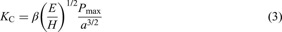
During the initial stages of the scratch process, the failure is more ductile with smooth scratch groves, especially when an indenter such as Rockwell C is used, which establishes a Hertzian (spherical) contact at the initial stages of loading. On proceeding further, the conical sides of the indenter start to make contact and a coexistence between ductile and brittle fracture exits with the formation of radial cracks and lateral cracks, which also propagate with a curvature as observed alongside the scratch tracks. The adhesive quality of a coating gets quantified by two critical loads Lc1 and Lc2 for cohesive and adhesive failure respectively. Chevron (radial) cracks (at an angle of 45°) representing the initiation of brittle failure can be seen in Figure 3(a) along the two cleaved sides of the track impression left by the indenter is representative of Lc1. Radial and lateral cracks can also be seen to have originated and propagated far from the scratch track. 22 Image analysis shows the groove of the radial crack to be around 5 µm, which is larger than the coating thickness, indicating that the substrate has been breached announcing adhesive failure. This points out the fact that although we consider deamination or chipping as proper evidence of adhesive failure, the process gets initiated much earlier though manifesting itself catastrophically later. A careful inspection therefore demands estimation of crack groove depths as a part of estimating coating adhesion.
(a) Formation of chevron cracks indicating brittle failure in the coating along with radial and lateral cracks with its (c, d) schema. (B) Brittle cleavage fracture along the scratch track in three different modes; pile up or plastic deformation sideways involving shear faults; a clear indication of ductile to brittle transition (DBT) of fracture. 22
The coating while getting deposited develops stress mainly due to differences in thermal expansion coefficients between the film and the substrate (extrinsic) or due to the generated defects or impurities in the coating. The surface is more prone to failure in the case of tensile stress. 23 A coating initially possessing compressive stress may develop tensile stress with an increase in thickness. Pre-existence of tensile stress promotes adhesive failure through chipping while compressive stress helps in radial cracking more. The presence of oxygen in the system for coatings where Si is one of the elements can be beneficial as the formation of SiO x can act as a buffer layer to accommodate the stress difference as also observed in the case of steels where SiOCN x films have been found compatible. The increased substrate temperature also promotes SiO x formation. 24
The total scratch region can be divided mainly into three regimes, starting with the micro-ductile having a smooth groove followed by the micro-cracking region which has been captured in Figure 3(a) showing the subsurface lateral and radial cracks. Evidence of any ductile failure cannot be seen in this region and there was also no evidence of any major delamination or buckling to have taken place indicating good adhesion. The last stage is the brittle regime causing chipping and spallation, where the lateral crack propagates to the surface to cause chipping. The stage captured in Figure 3(a) is the one just before the brittle failure, where an incomplete radial and lateral crack interaction happens to take place with a sideways extension and inflexion depicting a condition just before the phenomenon of chipping. This phenomenon reckons that the DBT starts in the process of transitions between the first two regimes and gets intensified further in the final regime experiencing predominant brittle failure. A schema showing the above events is given in Figure 3(c) and (d). As the films were about 1 µm thick, which was optimal due to avoiding any substrate influence and high stress at the coating–substrate interface causing poor adhesion, a cleavage fracture along with pile-up was observed indicating DBT fracture to have taken place as shown in Figure 3(b) with schema in Figure 3(e). 24
The stress field in the scratch test is a combination of Boussinesq (σBous) due to indenter loading, which has two components normal and tangential, and Blister (σBlister) stress fields due to residual stress. For the conical indenters, the normal component of σBous gets replaced by Hanso's field (σHans), which also causes the radial cracks. These principal stresses also have shear components associated with them as given in equations (4a) and (4b), where the superscripts n, t, and r represent ‘normal’, ‘tangential’ and ‘residual’. The lateral crack, which is mainly responsible for the brittle failure, is caused by σBlister. Due to residual tensile stress at the boundary between the plastic zone and the elastic body. The subsurface lateral cracks, however, occur only after the indenter has been removed from the sample surface.25,26


A complete brittle failure is evident from the formation of debris and spallation occurring due to the interaction of the radial and lateral cracks. A matter of deformation scale is evident from these observations as lowering the load increases the probability of ductile fracture. An increased brittleness has been reported to be indirect evidence of the lowering of adhesion.
27
An interesting observation of the formation of shear faults, however, prevailed in the chipped segments which again indicate localised plasticity to have emerged. A line profile indicated that the faults were on average 5 µm apart. These are also known as river lines and indicate the propagation of lateral cracks. This event took place due to the
Indenter tip sharpness
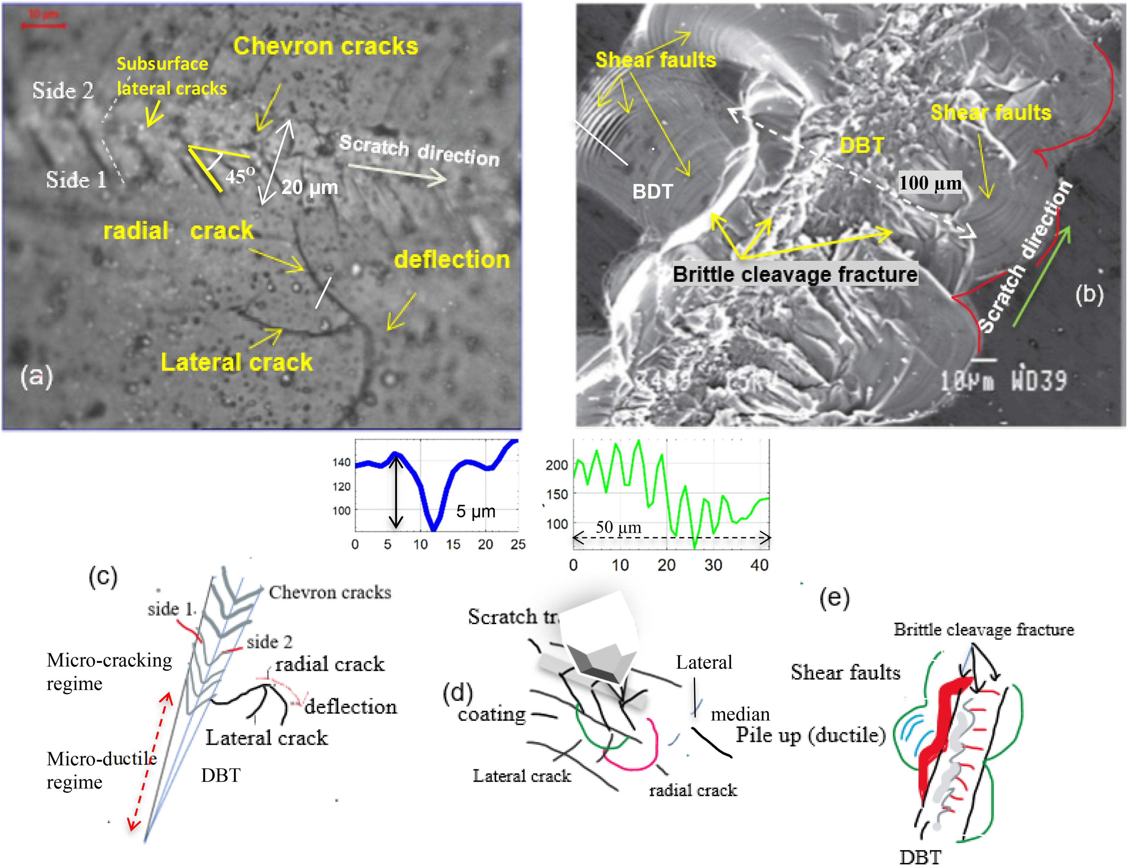
Tip sharpness has a significant role to play in nanoindentation. FEM analysis shows the shear stress distribution for Berkovich and cube-corner indenters, where the effect of stress is much broader and undistorted in the case of cube-corner indenters (Figure 4(a)). The stress originates at more than one region with variable magnitudes beneath the indentation as the tip sharpness is lowered. The smaller plastic zone regions associated with each of the originating regions lead to the interaction of the stresses causing overlapping and confinement at much lower depths as compared to cube-corner indentation (Figure 4(b)). Numerous dislocations are also observed which provide resistance to crack growth as the stress intensity is proportional to the square root of dimensional defects. The plastic zone near the crack tip is the dislocation distribution area with dimension
Shear stress distribution of (a) cube-corner indenter, (b) Berkovich indenter, and (c) TiN film. 23 (d) A high resolution transmission electron microscopy (HR TEM) image showing crystallisation with lattice fringes having d ∼ 2.6 Ȃ for (1 0 0) plane of TiB2 and pre-existing dislocations. 30 (e) Creation of a plastic zone in front of crack propagation. 23
Due to the higher sharpness of the cube-corner indenter, the hardness values are lower hence the plastic zone regions are higher. In both cases, resistance to the shear flow takes place at the film substrate interface changes its nature. This is also the region where charge carriers pass when the film/substrate system is configured in a microelectronic device. The constriction resistance Rc for Berkovich being smaller than that for the cube-corner indenter, the tip voltage will be much higher revealing the tip–sample electrical conduction. Similar studies involving FEM analysis have shown very high in-plane compressive stresses (∼10 GPa) in the film near-surface region next to the indenter. The formation of in-plane tensile stresses under the indenter can also be observed (Figure 4(c)). The changes in residual stress as the indenter penetrates the surface, influence the crack growth. The lattice fringes obtained from high resolution (HR) TEM image of Ti–B–Si–C films showing crystallisation having interplanar spacing d ∼ 2.6 Ȃ corresponding to (1 0 0) plane of TiB2 and pre-existing dislocations as shown in Figure 4(d). New or emitted dislocations are formed in the plastic zone created in front of the propagating crack tip (Figure 4(e)). 30 Even brittle oxides (MgO, ZrO2, and ZnO) deform solely plastically with dislocations under strong indenter points, as previously demonstrated. In a few cases, dislocation-governed plasticity was found during tests with sharp indenters, with a densification process accompanying dislocation activation (LiF, CaF2, SiC, ZrB2, and ZnS). High loads or indenters with a radius bigger than the plastic zone Rc cause cracks to form, triggering the DBT. (LiNbO3 and LiTaO3). The crack-related indentation size effect, also known as the indentation size-dependent BDT, states that shear strength is reached before fracture strength at ever-decreasing small scales with decreased fault density. 31
Dislocation kinetics
There exists a critical stress for DBT which is closely related to shear stress for dislocation motion (τy) that must be exceeded by the shear fracture stress (τf) during the indentation process for plastic to brittle transition to take place. At this stage, the load is high enough to cause work greater than the energy required to create dislocation (ΔHy). The dislocations are Shockley incomplete dislocations having two equal and opposite components b and −b. The first one (b) is generated at the edge of the plastic deformation and is immobile. The other component (−b) gets affected by the stress imposed and propagates along the slip system. 32 The yield stress (σy) as per Hall–Petch and fracture stress (σf) are related to the shear stress required for dislocation motion (τy) and shear fracture stress (τf), decide what kind of fracture, that is, DBT or BDT will occur for a particular material as per the temperature and grain size. Reducing the temperature (T) increases the ΔHy/kT ratio making the τy to reduce as τy ∼ exp (−ΔHy/kT), where k is the Boltzmann constant. This increases the probability of brittle fracture (Pf). A temperature rise, however, reverses the case. 33
Ductile–brittle–ductile transitions
For systems where nucleation and growth of small crystallites of different hard phases are involved, as in nanocomposite thin films, the phenomenon of DBT or BDT may take a different course of action as the increase in temperature has been found to produce coatings of increased mechanical strength due to growth of hard phases but followed an opposite trend after a certain critical temperature was exceeded. The reason is the continual growth of the crystallites by atomic diffusion from the nearby regions forming larger crystallites. A critical temperature, therefore, exists for the DBT. The proportion of DBT or BDT may therefore vary for different locations depending upon the nucleation topography of the region. However, a rough estimation can be drawn by the image analysis of the microstructure as shown in Figure 5. The image profiles of the regions (1, 2, and 3) marked in the TEM image as depicted in Figure 5(a) (Figure 1(a)) are shown separately in Figure 5(b) to (d). The down peaks shown by arrows indicate the crystallites that have nucleated during the deposition process on a matrix which may not be called amorphous but consists of ultrafine crystallites. It can be observed that taking a larger region has caused a diminishing of the peak intensities as the proportion of the matrix regions increases. The yield stress (σy) improves by five times when the crystallite size goes from micro to nano regime. However, a brittle fracture is more probable to occur as grain boundary sliding is non-existent. A fracture due to indentation performed on a region comprising a higher density of nucleated crystallites is therefore expected to be more ductile (BDT). The case gets reversed (DBT) for indentations performed in regions devoid of any significant nucleation. At this stage, the coating thickness and substrate will play a significant role.
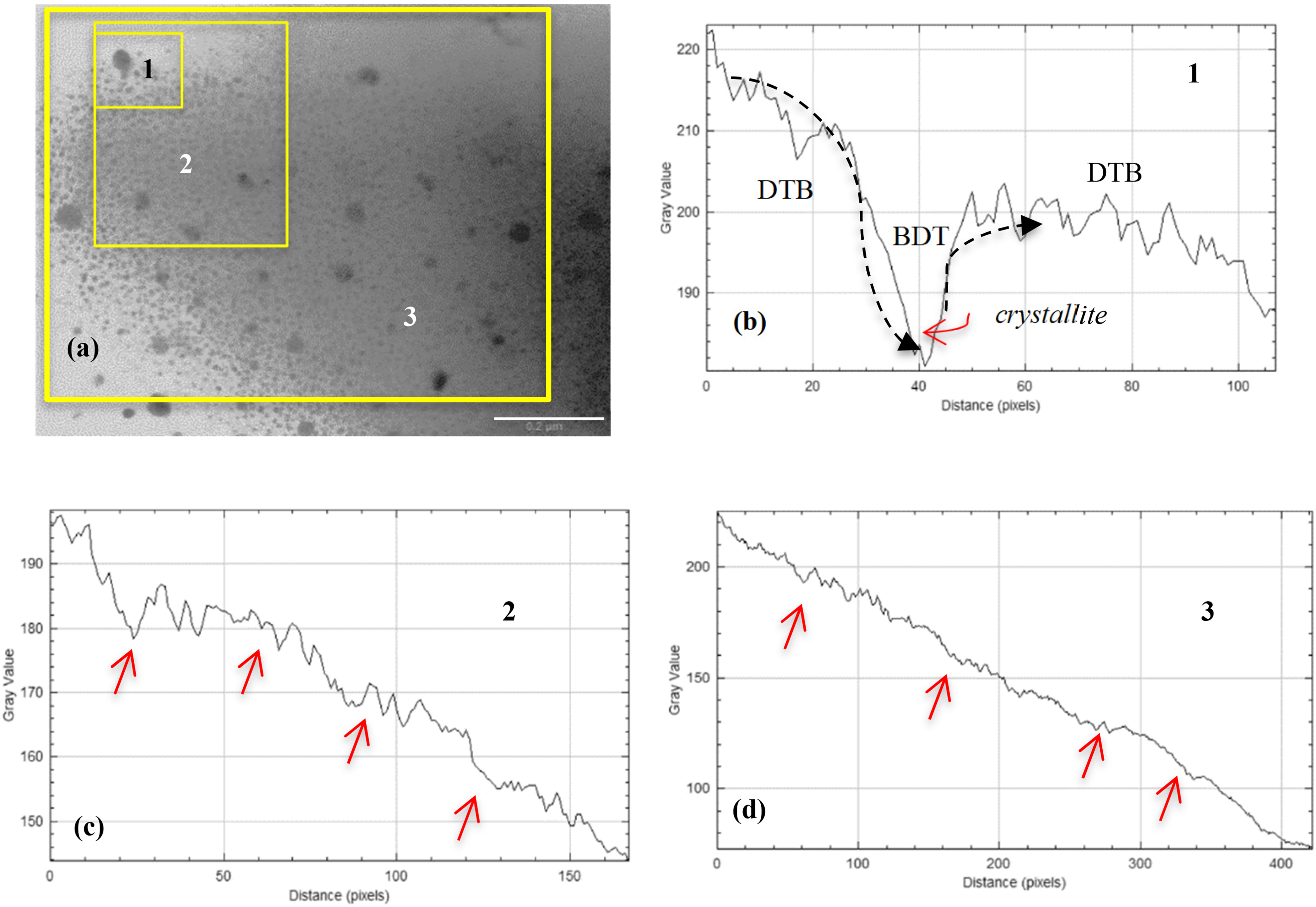
Image profiles for different regions as marked in (a) the TEM image (scale bar: 0.2 µm) 13 as (b) 1, (c) 2 and (d) 3 with peaks indicating the nucleated crystallites.
For hard coatings deposited on metals and alloys as protective coatings, the thickness is usually kept high (a few microns), which requires a higher deposition time, and consequently, a higher percentage of nucleated crystallites of hard phases will be present. So, the probability of ductile fracture is prevalent in this case unless the temperature is made low enough to cause the τy to go down causing a brittle fracture. For components being used in very high temperatures (close to 1000 °C), the dislocations as well as other defects such as vacancies are highly active and may lead to failure. Irradiation by inert metals (e.g. He) can cause embrittlement by restricting slip planes and grain boundary rotations. 34 The thickness of the coatings used in microelectronics or MEMS-based devices is much thinner (<500 nm) and therefore consists of a higher percentage of ultrafine crystallites. A brittle failure (DBT) is, therefore, more likely to occur in this case. A very recent study has shown a control on DBT by temperature which can be a future study for hard coatings. 35
Conclusions
Nanoindentation performed on SiCN coatings deposited on Si showed alteration in load-depth (P–h) responses due to heterogeneous crystallisation.
Inverse Hall–Petch rule came into existence in the amorphous phase.
The crystalline regions due to enhanced dislocation movement involved BDT failures.
The amorphous regions were more prone to DBT fractures.
The Pf varied between 0.094 for the crystallised regions to 0.52 for amorphous or near amorphous morphology.
Footnotes
Acknowledgement
The authors acknowledge the help of Dr S K Mishra, CSIR-NML for experimental facilities.
Author contributions
ASB wrote the manuscript. AKR helped in conceptualisation and KB performed the finite-element modelling.
Declaration of conflicting interests
The authors declared no potential conflicts of interest with respect to the research, authorship, and/or publication of this article.
Funding
The authors received no financial support for the research, authorship, and/or publication of this article.