
Abstract
In this work, the structural, optical, and electrical properties of Mn-doped ZnO thin films were systematically investigated. High-quality films were deposited on glass substrates using a spray pneumatic technique at 420 °C. X-ray diffraction analysis revealed that all films are polycrystalline with a hexagonal (wurtzite) structure and exhibit a strong (002) preferred orientation. Increasing Mn doping enhanced the film crystallinity, leading to a minimum crystallite size of 28.60 nm at 12% Mn. The films demonstrated good optical transparency in the visible range, with transmittance around 80%. As the Mn concentration increased from 3% to 12%, the optical band gap widened from 3.342 eV to 3.386 eV, while the Urbach energy reached a maximum value of 0.362 eV at 12% Mn, indicating increased structural disorder. Additionally, the electrical resistance of the films increased significantly from 1.13 × 10⁶ Ω to 2.13 × 10⁶ Ω with higher Mn doping. These results suggest that Mn-doped ZnO thin films are promising candidates for optoelectronic and gas sensor applications due to their tunable structural, optical, and electrical properties.
Introduction
In recent years, zinc oxide (ZnO) has gained significant interest owing to its high optical transparency and favorable electrical conductivity. Its transmittance, often exceeding 90% in the visible region, makes it particularly suitable for gas sensing and transparent electronic applications.1–4 ZnO is a prominent binary II–VI semiconductor extensively studied for its optoelectronic versatility and widely employed in devices such as light-emitting diodes, laser diodes, and acousto-optic systems. The material exhibits a wide direct band gap of 3.37 eV and a high exciton binding energy of 60 meV, contributing to its efficient optical performance and thermal stability. These intrinsic characteristics enhance its suitability for advanced optoelectronic and photonic applications requiring high transparency and conductivity.2–7
Doping with elements such as Al, Cu, Ag, Co, In, Sn, Fe, and F significantly modifies the optical and electrical properties of ZnO thin films. For instance, Mn incorporation enhances optical transmittance, widens the optical band gap, and reduces structural disorder. In addition, doping with Mn improves electrical conductivity while enabling precise tuning of the band gap and Urbach energy. These modifications considerably expand the potential of doped ZnO thin films for advanced optoelectronic and transparent conductive applications.
The influence of Mn doping on the structural, optical, and electrical properties of ZnO thin films was systematically investigated. The films were deposited on glass substrates via pneumatic spray pyrolysis at 400 °C, using a precursor solution with a molarity of 0.1 mol·L⁻1.
Experimental
In this work, Zinc acetate dihydrate (Zn(CH3COO)2, 2H2O) (industrial powder) was used to prepare the ZnO solution with 0.15 M, however, Manganese chloride dihydrate (MnCl3, 2H2O) (industrial powder) was used to prepare the MnO solution with 0.15 M. the solutions were dissolved in a volume equal to water. Three drops of sodium hydroxide (NaOH, 99.7% purity) were added to the ZnO and MnO solutions to stabilize the pH at 7. The solutions were then heated to 50 °C to obtain a homogeneous, transparent, and well-prepared precursor solution suitable for thin film deposition
The resulting Mn-doped ZnO solution was used to prepare thin films via the pneumatic spray method. Mn-doped ZnO thin films were deposited on R217102 microscopic glass substrates (75 × 25 × 1.2 mm3), which have been tested to withstand temperatures up to 620 °C. The precursor solution was atomized into a uniform stream of fine droplets with an average diameter of 30 µm. Mg doping was introduced at concentrations of 3, 6, 9, and 12 wt% (see Table 1). The films were deposited at a substrate temperature of 420 °C by spraying 25 mL of the solution over a period of approximately 25 min.
Experimental conditions for the deposition of Mn-doped ZnO thin films at various Mn doping ratios.
The structural, optical, and electrical properties of Mn-doped ZnO thin films were investigated using X-ray diffraction (XRD, Bruker AXS-8D) with CuKα radiation (λ = 0.15406 nm), recorded over a 2θ range of 25°–50° with a step size of 0.015° and a scanning time of 45 min. Optical measurements were performed using a UV–Vis spectrophotometer (Lambda 35) in the wavelength range of 350–1000 nm. The electrical properties were evaluated using the four-point probe method with a Keithley Model 2400 low-voltage source meter.
Results and discussion
Figure 1 illustrates the effect of Mn-doping on the structural properties of ZnO thin films. The X-ray diffraction (XRD) patterns reveal four distinct diffraction peaks at different angles, which are consistent with the standard JCPDS data (card no. 36–1451). 8 These results confirm that the films exhibit a hexagonal wurtzite structure. 9 The most intense peaks are observed at 2θ ≈ 34.5° and 36.5°, corresponding to the (002) and (101) crystallographic planes, respectively. This indicates that the preferred orientation is mainly along these directions. Furthermore, the presence of multiple diffraction peaks suggests that the Mn-doped ZnO thin films possess a polycrystalline nature.
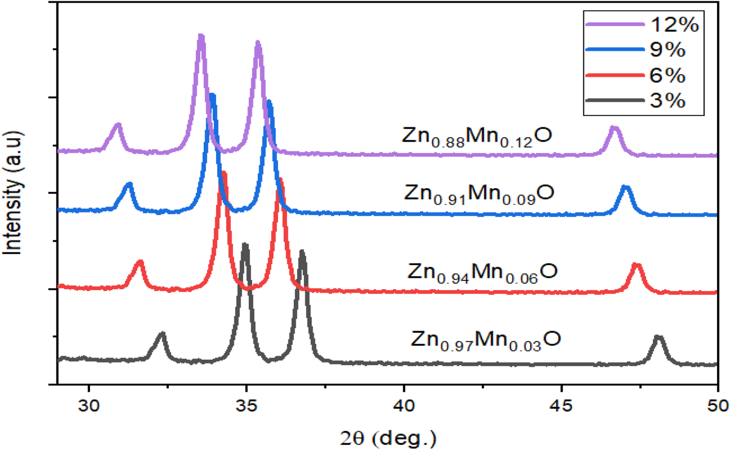
X-ray diffraction (XRD) patterns of Mn-doped ZnO thin films at different Mn doping ratios.
The texture coefficient of Mn-doped ZnO thin films is determined from X-ray diffraction data by analyzing the intensities of the main diffraction peaks, particularly those associated with the (100), (002), (101), and (102) crystallographic planes, according to the standard relation
10
:
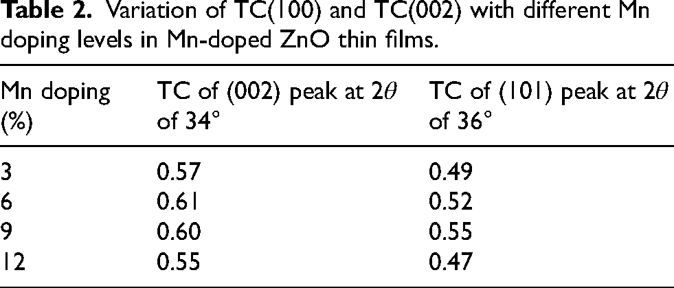
Variation of TC(100) and TC(002) with different Mn doping levels in Mn-doped ZnO thin films.
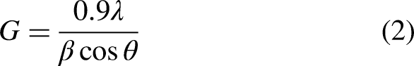
In this study, the crystallite size of Mn-doped ZnO thin films was evaluated based on X-ray diffraction data using the Debye–Scherrer equation
11
:
Variation of the crystallite size of three crystallographic planes of Mn-doped ZnO thin films with varying Mn doping levels.
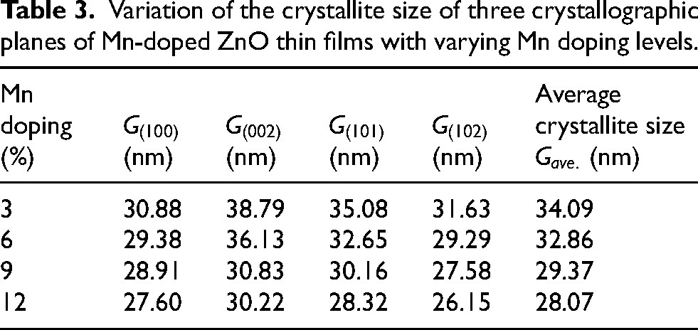
The variation of crystallite size for different crystallographic planes of Mn-doped ZnO thin films as a function of Mn doping concentration is illustrated in Figure 2. It is clearly observed that the crystallite size decreases gradually with increasing Mn content for all diffraction planes ((100), (002), (101), and (102)). The (002) plane exhibits the highest crystallite size compared to other planes, confirming that the films are preferentially oriented along the c-axis. This dominant orientation is typical for ZnO with a hexagonal wurtzite structure. The reduction in crystallite size with increasing Mn doping can be attributed to the substitution of Zn + 2 ions by Mn + 2 ions, which introduces lattice distortions and inhibits crystal growth. Additionally, the presence of Mn ions may act as defects or nucleation centers, leading to the formation of smaller crystallites. A similar decreasing trend is also observed for the average crystallite size, indicating that Mn incorporation significantly affects the microstructural properties of the films. This behavior is consistent with previous studies reported in the literature, where dopant incorporation limits grain growth and enhances structural disorder.
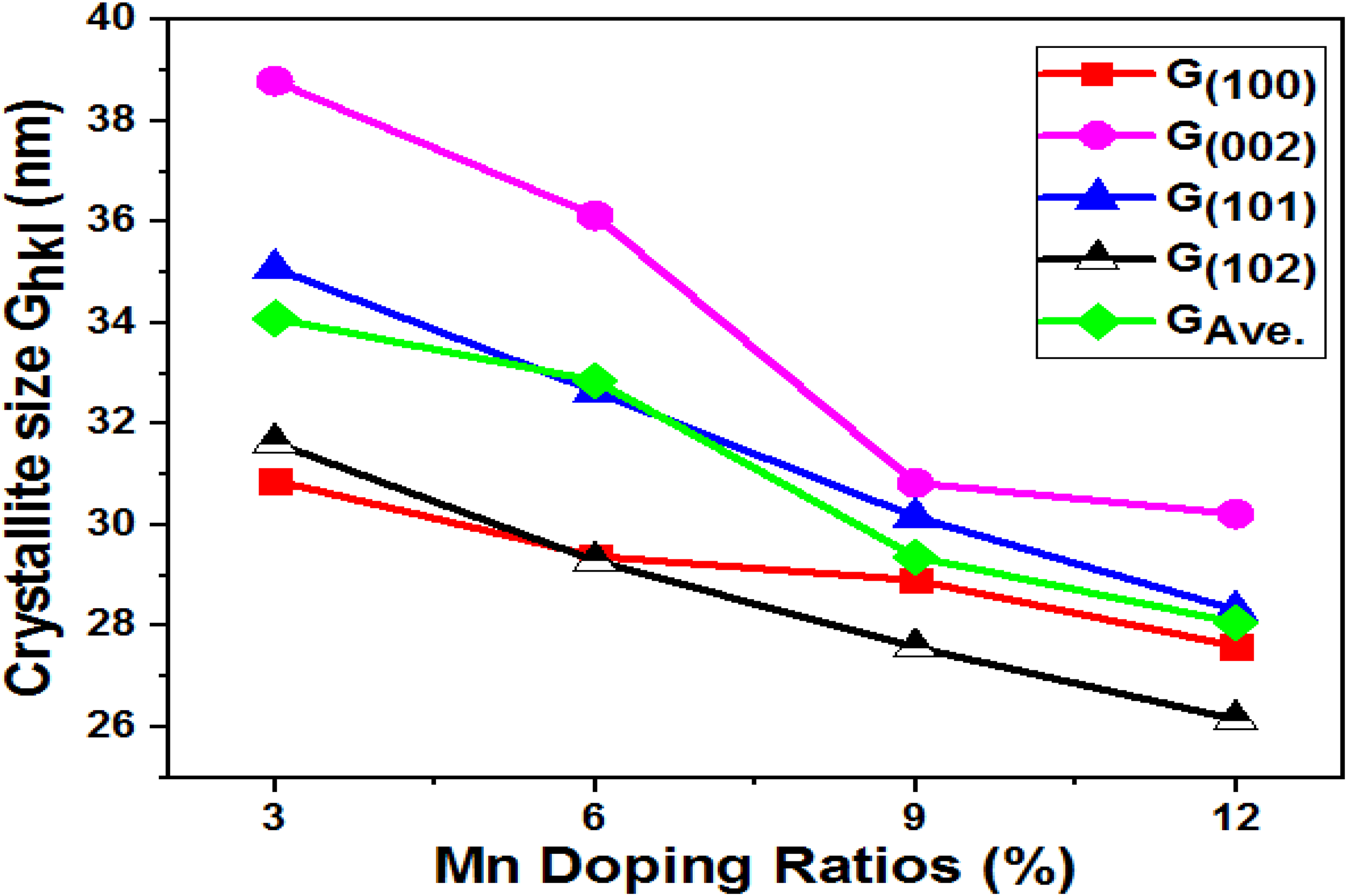
Evolution of crystallite size for the (100), (002), (101), and (102) planes of Mn-doped ZnO thin films with increasing Mn doping concentration.
Figure 3 presents the optical transmittance spectra of Mn-doped ZnO thin films as a function of Mn doping levels (3, 6, 9, and 12%). For wavelengths greater than 400 nm, all deposited films exhibit high transparency, with an average transmittance of approximately 80%. A gradual decrease in transmittance is observed with increasing Mn doping concentration, which may be attributed to an increase in film thickness or enhanced scattering effects. In contrast, for wavelengths below 400 nm, the transmittance significantly decreases due to the onset of fundamental absorption associated with electronic transitions from the valence band to the conduction band.
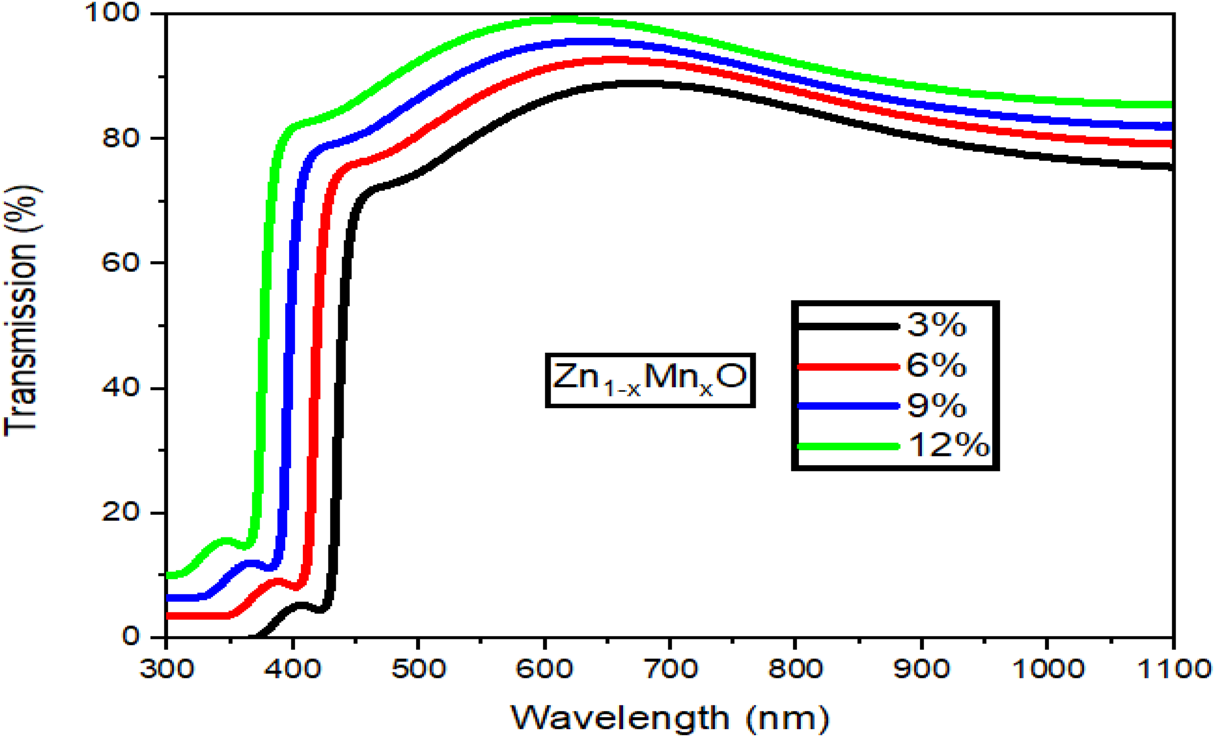
Variation of optical transmittance of Mn-doped ZnO thin films as a function of Mn doping concentration.
Figure 4 shows the absorbance spectra of Mn-doped ZnO thin films. It is observed that the absorbance remains low at wavelengths greater than 400 nm, indicating high transparency in the visible region. However, at shorter wavelengths, the absorbance increases significantly, accompanied by a noticeable rise in the absorption edge. A clear blue shift in the absorption edge is observed with increasing Mn doping, suggesting a widening of the optical band gap. This behavior may be attributed to changes in the electronic structure induced by doping. Furthermore, the results indicate that the optical transparency of the films is influenced by the Mn doping concentration.
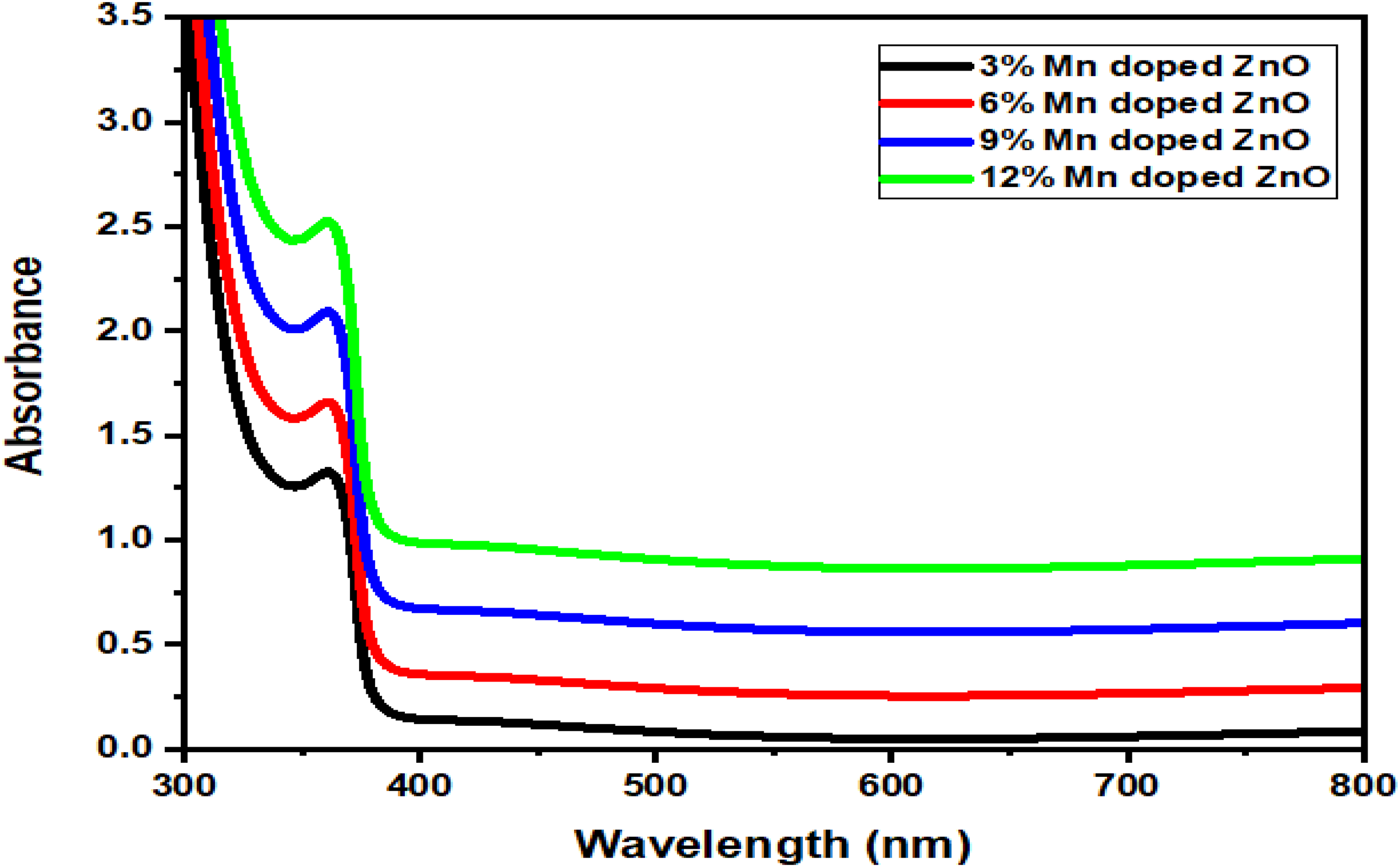
Variation of optical absorption of Mn-doped ZnO thin films as a function of Mn doping concentration.
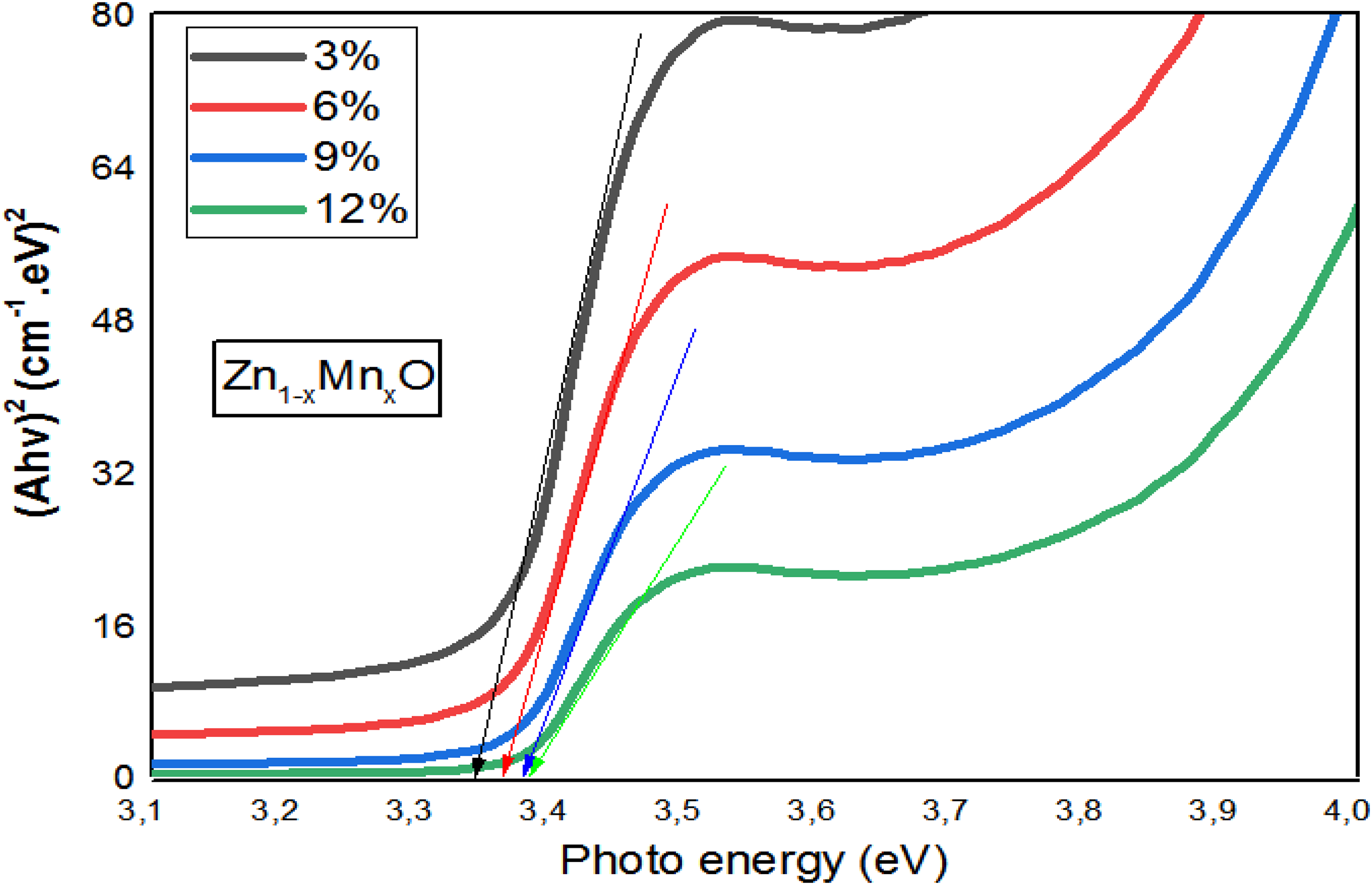
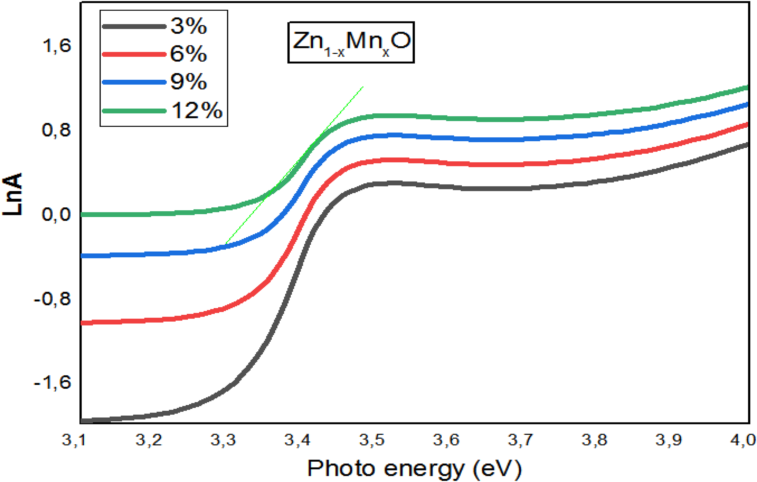
The optical band gap energy 

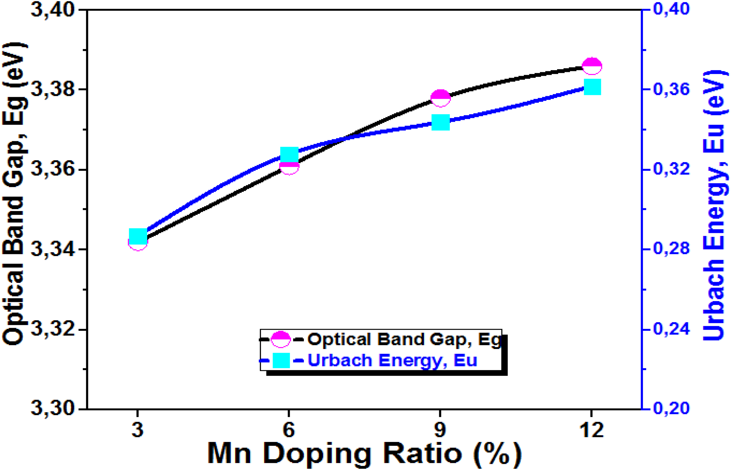
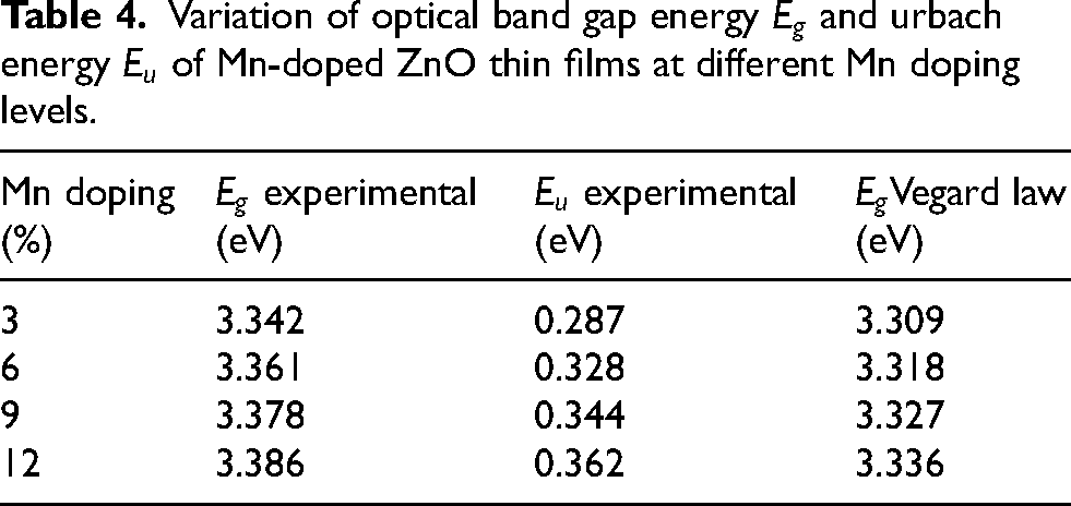
Figure 7 shows the variation of the optical band gap and Urbach energy of Mn-doped ZnO thin films as a function of Mn doping levels (3, 6, 9, and 12%). The band gap was observed to increase slightly with increasing Mn content, ranging from 3.342 to 3.386 eV (see Table 4). In contrast, the Urbach energy increased from 0.287 to 0.362 eV as the Mn doping increased from 3 to 12%, which can be attributed to the reduction in crystallite size (see Table 3). Furthermore, the optical band gap was compared with the predictions of Vegard's law, showing good agreement with this model (see Table 4). The following equations were applied for the analysis: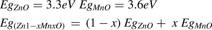
The typical variation of
The variations
Variation of optical band gap energy
Variation of optical band gap energy
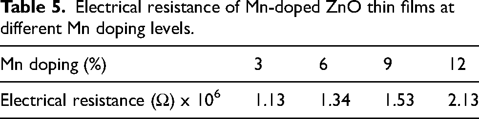
The electrical properties of Mn-doped ZnO thin films were investigated using the four-point probe method at room temperature. Figure 8 shows the current–voltage (I–V) characteristics, which exhibit a linear relationship between voltage and current in the range of 0–60 nA. The measured voltage increases with increasing Mn concentration, indicating a variation in electrical resistance. Among the samples, the lowest resistance was observed for the film doped with 3% Mn. The electrical resistance (R) of the Mn-doped ZnO thin films was calculated using relation (7), and the results are summarized in Table 5.
14
Overall, an increase in electrical resistance was observed with higher Mn doping levels.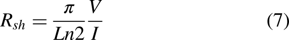
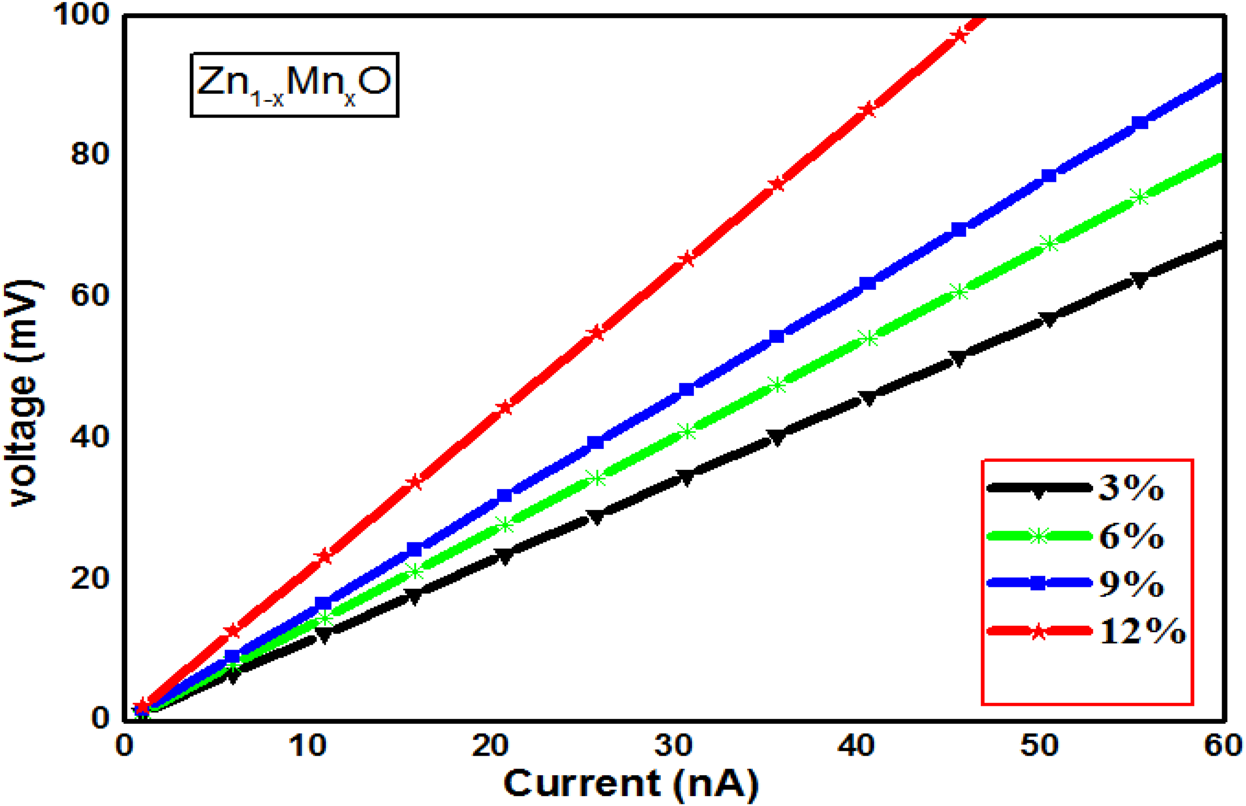
Voltage changes in terms of current intensity at various concentrations.
Electrical resistance of Mn-doped ZnO thin films at different Mn doping levels.
Conclusions
In this study, the structural, optical, and electrical properties of Mn-doped ZnO thin films were systematically investigated. High-quality Mn-doped ZnO thin films were successfully deposited on glass substrates using the spray pneumatic technique at a substrate temperature of 420 °C. The main conclusions drawn from this work are summarized as follows:
The XRD patterns of Mn-doped ZnO thin films indicate that they are polycrystalline with a hexagonal wurtzite structure and a pronounced (002) preferred orientation. Increasing the Mn doping concentration improved the film structure, resulting in a minimum crystallite size of 28.60 nm at 12% Mn. The Mn-doped ZnO thin films exhibit high optical transparency in the visible region, with an average transmittance of approximately 80%. Increasing the Mn concentration from 3% to 12% resulted in a slight increase in the optical band gap from 3.342 to 3.386 eV. Additionally, the film doped with 12% Mn exhibited the highest Urbach energy of 0.362 eV, indicating increased structural disorder at higher doping levels. The electrical resistance of Mn-doped ZnO thin films increased significantly with higher Mn doping, rising from 1.13 × 10⁶ to of 2.13 × 10⁶ Ω as the Mn concentration increased. Finally, Mn-doped ZnO thin films with optimized doping levels are suitable for use as the active layer in gas sensors due to their high optical transparency and favorable electrical conductivity.
Footnotes
Funding
The authors received no financial support for the research, authorship, and/or publication of this article.
Declaration of conflicting interests
The authors declared no potential conflicts of interest with respect to the research, authorship, and/or publication of this article.