
Abstract
An unsymmetrical switch circuit is designed for semi-active control method based on synchronized switching damping principle of piezoelectric actuators. A bypass capacitor and an additional switch are used to realize unsymmetrical bipolar voltage. The control logic of the switches is introduced in detail and the switched voltages, which directly influence the control performance, are derived as functions of the vibration amplitude and the outputs of the voltage sources. Experiments were carried out to verify the designed circuit and the theoretical results of the switched voltage. For simplification of experimental conditions, the beam is fully clamped and the voltage is fully generated by the voltage source. The influence of the voltage source and bypass capacitor on the actuator was investigated. Experimental results show that the circuit leakage is a critical factor to the amplification of actuator voltage. The voltage ratio increases with increasing bypass capacitance, but its increasing rate decreases.
Keywords
Introduction
Structural vibration control has been an active research area since early 1990s (Hagood et al., 1990; Tani et al., 1998). The methods of structural vibration control can be divided into three categories: active, passive, and semi-active (Qiu et al., 2009). Passive methods have the advantages of low weight and compact size, but have the disadvantage of low robustness (Hollkamp, 1994). Active methods have the advantages of high control performance and robustness, but have the disadvantages of requiring high-performance digital signal processors and bulky power amplifiers. In order to overcome these disadvantages, several semi-active approaches have been proposed. Wang et al. (1996) studied a semi-active R–L shunting approach, in which an adaptive inductor tuning, a negative resistance, and a coupling enhancement setup led to a system with damping ability. Davis et al. (1997) developed a tunable electrically shunted piezoceramic vibration absorber, in which a passive capacitive shunt circuit is used to electrically change the piezoceramic effective stiffness and then to tune the device response frequency. Clark (1999) proposed a state-switched method, in which piezoelements are periodically held in the open-circuit state and then switched and held in the short-circuit state, synchronously with the structure motion.
Another type of semi-active control, which has been receiving much attention in recent years, is called pulse switching technique (Onoda et al., 2003; Richard et al., 1998). It consists of a fast inversion of voltage on the piezoelement using a few basic electronics, which is synchronized with the mechanical vibration. In the methods proposed by Richard et al. (1998), the voltage on the piezoelectric element is switched at the strain extrema or displacement extrema of vibration. These methods are called synchronized switch damping (SSD) techniques. On the other hand, in the method proposed by Onoda et al. (2003), the switch is controlled by an active control theory, and it is called active control theory–based switching technique here.
In the original SSD technique, the control performance mainly depends on the value of the voltage on piezoelectric element. To improve the control performance, an inductance can be connected to the shunt circuit to invert the voltage in the piezoelectric patch. This method is called synchronized switch damping on inductor (SSDI). The inversion process boosts the voltage, thus increasing energy dissipation. The objective of all switch control algorithms is to maximize the energy dissipated in each cycle of vibration. To further improve the control performance, a method called synchronized switch damping on voltage (SSDV) has been proposed (Badel et al., 2006; Lefeuvre et al., 2006).
Due to the inherent properties of piezoelectric materials, the applicable bipolar voltage of a piezoelectric actuator is unsymmetrical. That is, the voltage applicable in the positive direction (poled direction) is much higher than that in the negative direction. Otherwise, the actuator is depoled. The typical electric field applicable in the positive direction is higher than 2000 V/mm, but that in the negative direction is only about 500 V/mm. As an example of applicable voltage on an actuator, the working voltage range of micro-fiber composite (MFC) actuator is from −500 to 1500 V. If symmetrical switching circuit is used, the voltage range will be from −500 to 500 V so that half of the actuator capability will be wasted.
In this article, an unsymmetrical switch circuit is designed for semi-active control method based on synchronized switching damping principle of piezoelectric actuators. A bypass capacitor and an additional switch are used to realize unsymmetrical bipolar voltage. The control logic of the switches introduced in detail and the switched voltages, which directly influence the control performance, are derived as functions of the vibration amplitude and the outputs of the voltage sources. Simulations and experiments were carried out to verify the design circuit and the theoretical results of the switched voltage.
Principle of unsymmetrical SSD methods
Electromechanical model of a vibration system
A mechanical model based on a spring–mass system having only 1 degree of freedom, which is shown in Figure 1, gives a good description of the vibrating behavior of a structure near a resonance (Badel et al., 2007; Lallart et al., 2008). The following differential equation is established assuming that the global structure including piezoelectric elements is linearly elastic

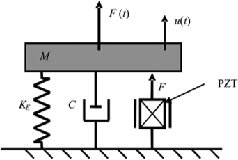
A single DOF with a piezoelectric transducer.
where M represents the equivalent rigid mass, C is the inherent structural damping coefficient, and KE is the equivalent stiffness of the structural system, which can be expressed as

where


where Fp is the electrically dependent part of the force applied by piezoelectric elements on the structure, Va is the voltage on the piezoelectric elements, Cp is the blocked capacitance of piezoelectric elements, α is the force factor, and I is the outgoing current from piezoelectric elements. M, Cp, α and KE can be deduced from piezoelectric elements and structure characteristics and geometry.
Finally,

The following energy equation is obtained by multiplying both sides of the above equation by the velocity and integrating it over the time variable
This equation exhibits that the provided energy is divided into kinetic energy, potential elastic energy, mechanical losses, and transferred energy. In the steady-state vibration, the terms of potential energy and kinetic energy in equation (6) disappear. The provided energy is balanced by the energy dissipated on the mechanical damper and the transferred energy, which corresponds to the part of mechanical energy which is converted into electrical energy. Maximizing this energy amounts to minimize the mechanical energy in the structure (kinetic + elastic).
Review of the symmetrical switch circuit
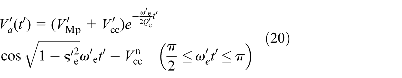
A typical switch circuit for the SSDV method is shown in Figure 2(a), and the corresponding actuator voltage is shown in Figure 2(b). If there are no voltage sources in the circuit, it becomes the switch circuit of SSDI control. Between the actuator voltages
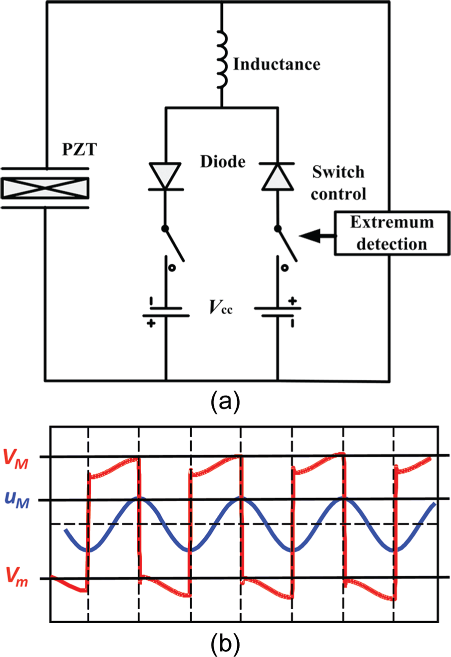
The principle of SSDV: (a) the schematic of a SSDV circuit and (b) the waveforms of actuator voltage and displacement.
where

From equation (7), the following switched voltage can be obtained
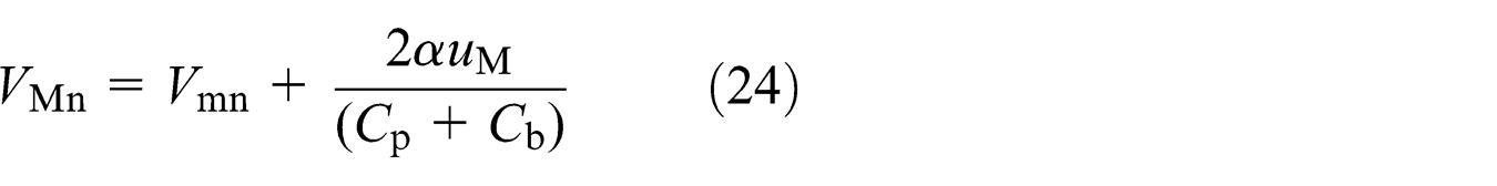
The switched voltage can be effectively raised by increasing the output of the voltage source
In steady-state control, the converted energy in a cycle of vibration can be expressed as
The above expression indicates that the converted energy is proportional to the amplitude of switched voltage. In the conventional symmetrical switching, the switched voltage is limited by the applicable voltage in the negative direction of piezoelectric actuator. If unsymmetrical switching is used, then the converted energy in each vibration cycle can be further increased and the control performance can be improved.
Principle of unsymmetrical methods
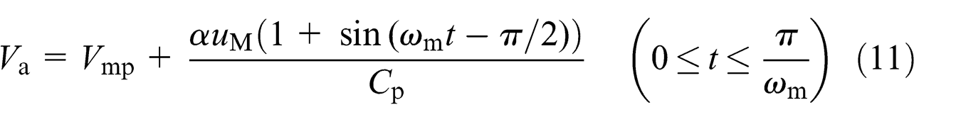
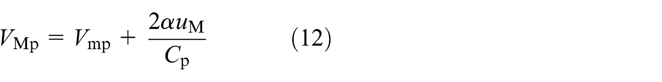
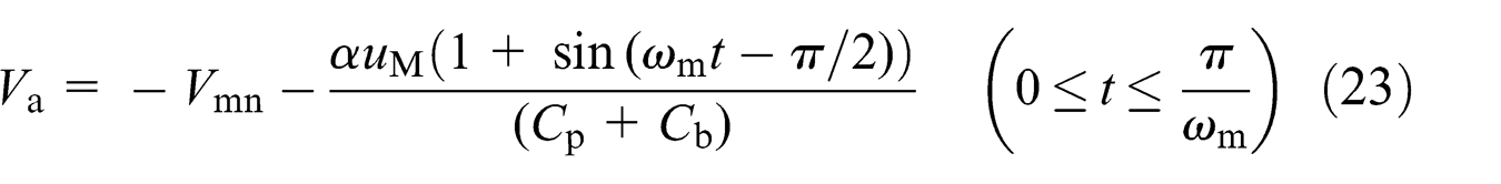
The schematic diagram of the designed unsymmetrical SSDV control system is shown in Figure 3. The difference is that a unidirectional bypass capacitor is connected in parallel to the lead zirconium titanate (PZT) actuator. The polarity of the PZT actuator is labeled by “+” and “−” in the figure. The schematic diagram of the switched voltage is shown in Figure 3(b). The positive voltages just after and before switching action are expressed as Vmp and VMp, and the absolute values of negative voltages just after and before switching action are denoted by Vmn and VMn. In order to obtain unsymmetrical actuator voltage, the switching logic shown in Figure 4 is used to control the three switchers. In one cycle of vibration, the voltage is inverted twice. The variation of voltage on the PZT actuator can be divided into six phases. Due to the second-order characteristic of the shunt circuit for voltage inversion, the voltage and current are continuous at the boundary between every two phases. In the following analysis, control of steady-state resonant vibration is considered. That is, the displacement is assumed to a sinusoidal function of time t expressed as

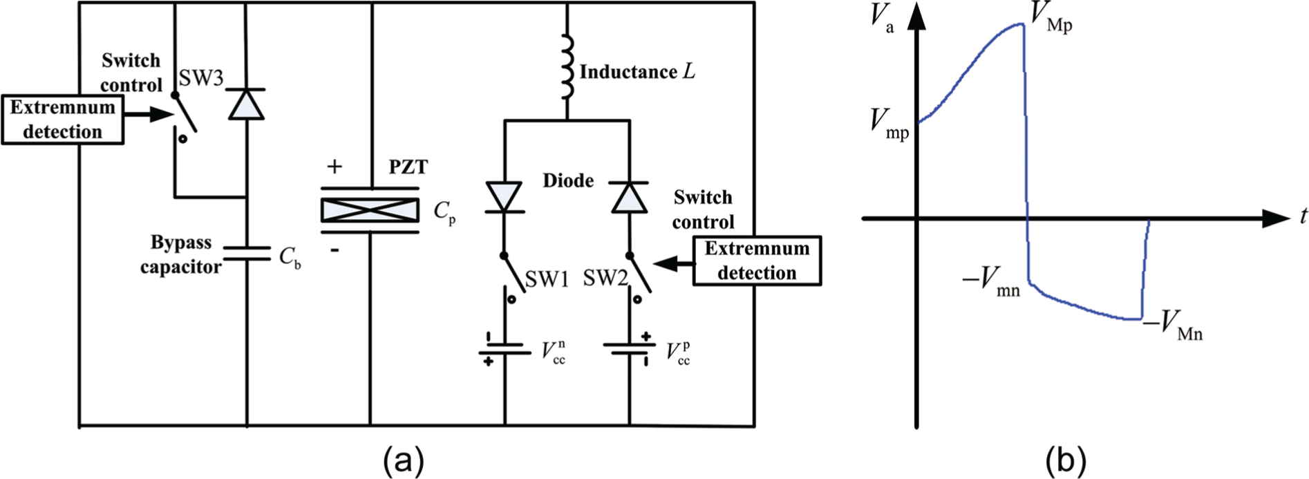
Principle of unsymmetrical switch circuit: (a) the schematic of an unsymmetrical switch circuit and (b) the actuator voltage.
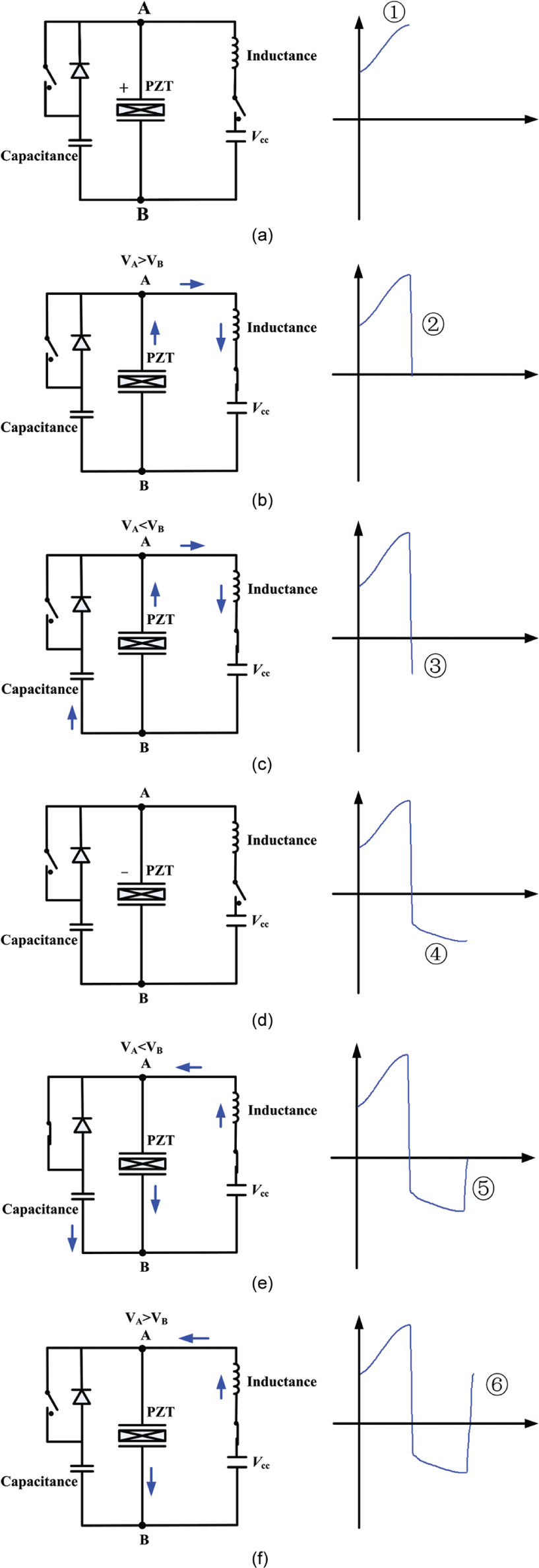
Switching logic of the unsymmetrical switch circuit: (a) Phase 1—voltage increasing as displacement changes from minimum to maximum, (b) Phase 2—voltage inverted from positive to negative with bypass capacitor open, (c) Phase 3—voltage inverted from positive to negative with bypass closed, (d) Phase 4—voltage decreasing as displacement changes from maximum to minimum, (e) Phase 5—voltage inverted from negative to positive with bypass closed, and (f) Phase 6—voltage inverted from negative to positive with bypass open.
where its frequency equals the natural frequency of the mechanical system.
Displacement increasing from minimum to maximum (Phase 1)
After the switching action is finished at the displacement minimum, the voltage on the PZT actuator is positive. All the switchers are open and the voltage increases as the displacement increases from minimum to maximum. The voltage on the bypass capacitor is 0 because the current is blocked by the diode, that is, I = 0. Integrating equation (4) yields
where
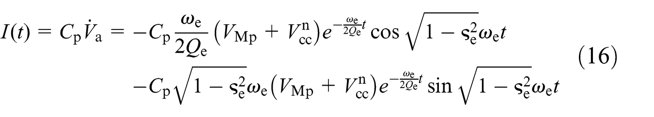
Voltage inversion at displacement maximum with bypass capacitor open (Phase 2)
At the displacement maximum, switch SW1 is closed and voltage inversion starts. The electric current flows through the loop as shown in Figure 4(b). The current on the bypass capacitor is 0 in Phase 2 because it is blocked by the diode when the voltage on the PZT actuator is positive. Normally, in SSD control, the resonance frequency of the circuit,

where L is the inductance, Cp is the capacitance of the piezoelectric element, R is the inherent resistance of the shunt circuit, and

The voltage can be expressed in the following form
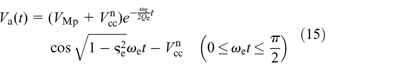
where
Here, it is assumed that
The boundary between Phase 2 and Phase 3 is the moment at which

If

Voltage inversion at displacement maximum with bypass capacitor closed (Phase 3)
In Phase 3, the voltage on PZT actuator becomes negative and the current will flow through both the PZT actuator and the bypass capacitor, as shown by the arrows in Figure 4(c). Because the voltage between the two sides of the diode is almost 0, the voltage on the bypass capacitor is approximately the same as that on the PZT actuator. Hence, the voltage on the PZT actuator satisfies in the following equation

The voltage can be expressed in the following form
where
where
At the end of Phase 3, the voltage is
Displacement decreasing from maximum to minimum (Phase 4)
After the switching action is finished at the displacement maximum, the voltage on the PZT actuator is negative. All the switchers are open and the voltage decreases as the displacement decreases from maximum to minimum. The voltage on the bypass capacitor is the same as that in the PZT actuator. Hence, the actuator voltage is
After half a cycle of mechanical vibration, the displacement reaches its minimum and the voltage on the PZT actuator reaches VMn. Hence, there exists
Voltage inversion at displacement minimum with bypass capacitor closed (Phase 5)
In Phase 5, both SW2 and SW3 are closed so that the PZT actuator and the bypass capacitor are discharged simultaneously, as shown by the arrows in Figure 4(e). The voltage on PZT actuator increases from VMn to 0. The voltage on the PZT actuator satisfies

where

The voltage can be expressed in the following form
If

If

Voltage inversion at displacement minimum with bypass capacitor open (Phase 6)
In Phase 6, switcher SW2 is kept in the closed state, but SW3 is opened. Hence, the electric current flows only through the loop as shown in Figure 3(f) and the voltage on the PZT actuator satisfies

The voltage can be expressed in the following form
Using the condition that the voltage and current at the beginning of Phase 6 are the same as those at the end of Phase 5, shown in equation (28) for
At the end of Phase 6, the voltage is
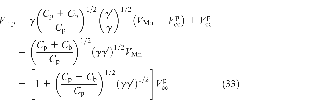
Voltages before and after switching
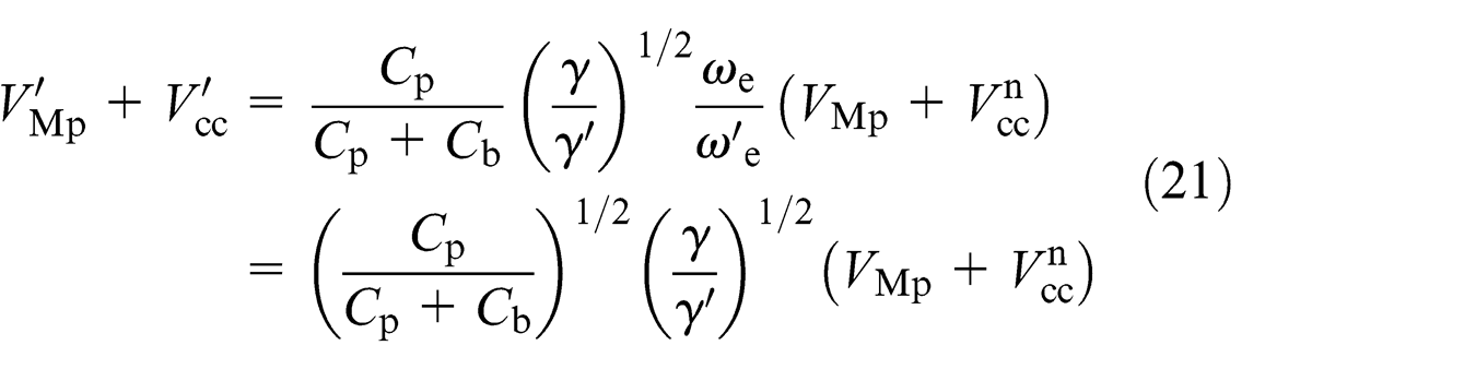
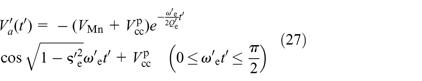
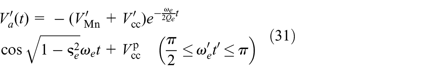
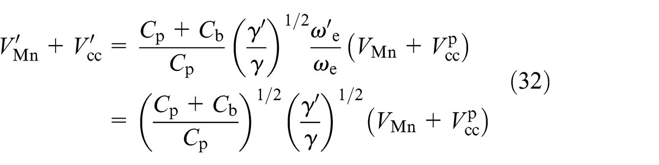
The relationships between the voltages before and after switching have been derived in the former section. In this study, the voltages before and after switching are expressed as functions of the vibration amplitude and the voltage sources. Consequent substitution of equations (33), (24), and (22) into equation (12) yields
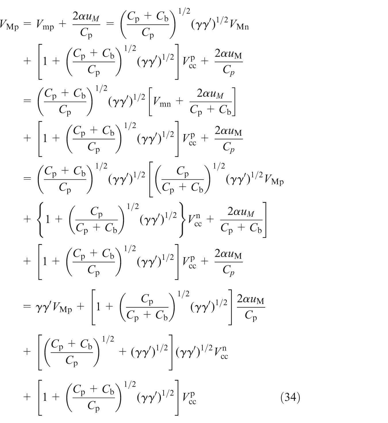
Solution of
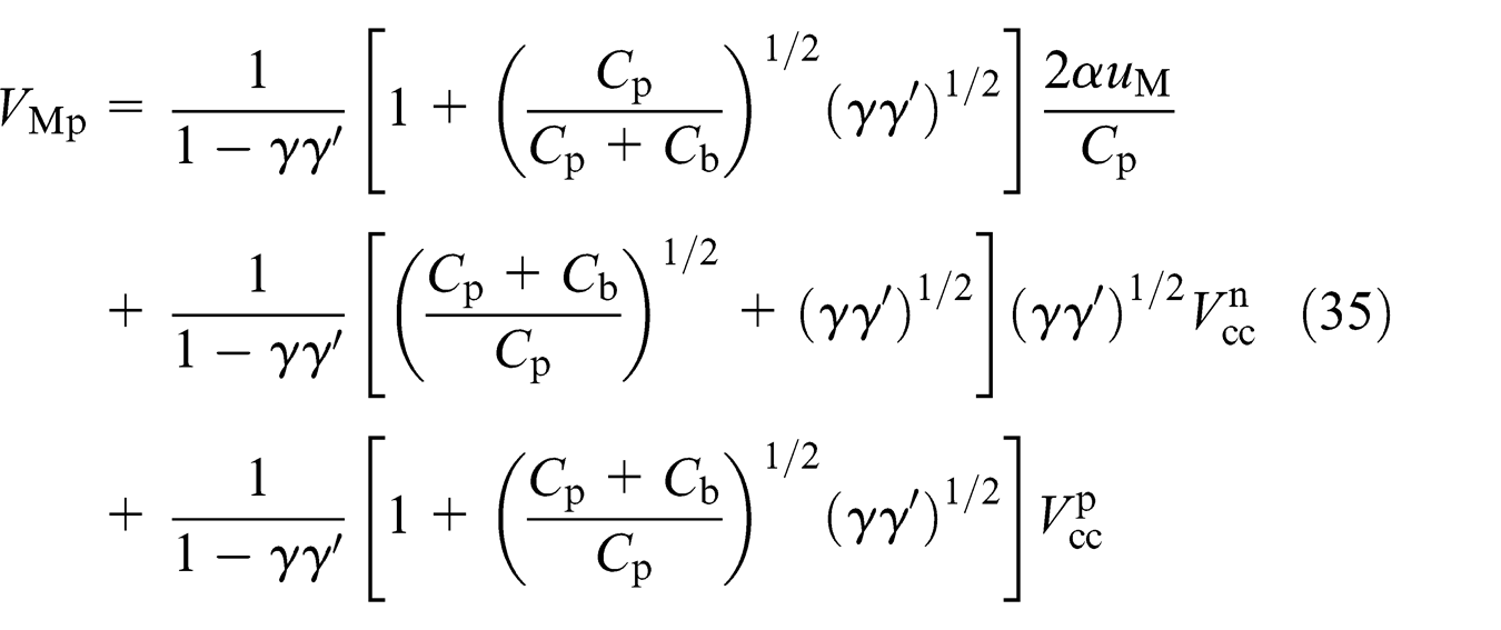
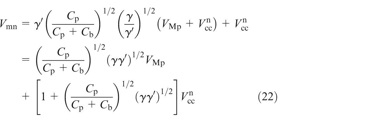
Using the same method, VMn can be obtained
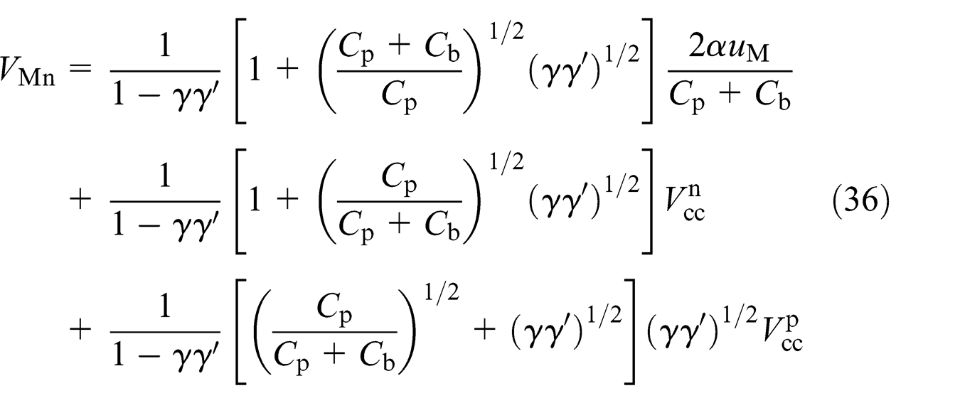
The control effect depends on the switch voltages
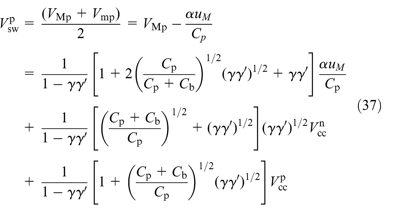
and
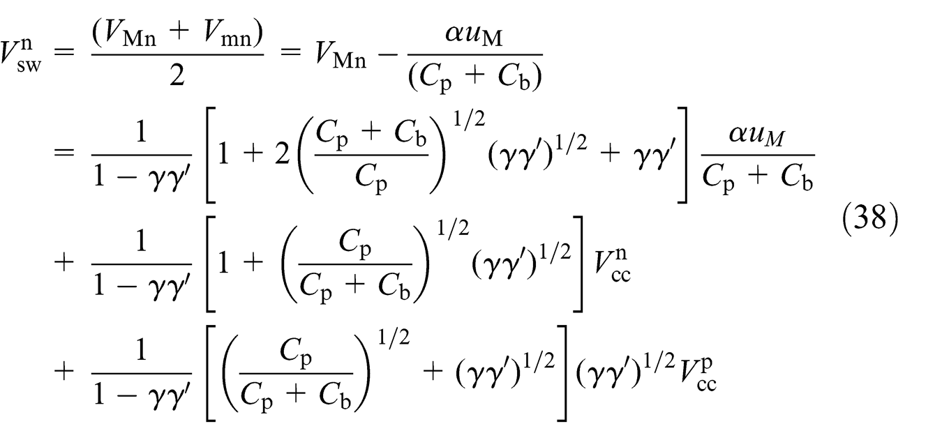
The unsymmetrical voltage ratio is defined as
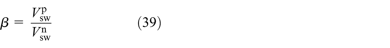
Equations (37)–(39) indicate that voltage ratio β depends mainly on the bypass capacitor
Verification experiments and simulation
Experimental and simulation conditions
A composite beam was used in the experiments as shown in Figure 5 (Ji et al., 2009). It has two embedded piezoelectric elements, the capacitance of which is 141 nF. In order to simplify the verification of the circuit, the beam is fully clamped so that no bending deformation was generated in the beam, that is, um = 0. The voltage on the piezoelectric element was generated by the voltage source. Because the vibration of the beam was fully suppressed, the voltage is switched at a hypothetical frequency, 2 Hz, which is different from the natural frequency.
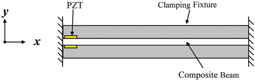
The experimental setup: a composite beam with piezoelectric patches.
A Simulink model of the system including the structure, the piezoelectric actuator, and the switching circuit was established. The parameters used in the simulation are shown in Table 1. The actuator voltage with symmetrical and unsymmetrical switching circuits can be directly obtained from the simulation model. The quality factor is
Parameter of the system.
lead zirconium titanate
Experimental and simulation results
Symmetrical switching
First, the bypass capacitor is disconnected and the symmetrical switching case is considered. The output of the voltage source was increased from 0 to 20 V and the voltage on the piezoelectric actuator was measured. The waveform of the voltage is shown in Figure 6 when Vcc = 15 V. Although rectangular waveform was expected on the piezoelectric actuator, the voltage is not constant when the switch is in the open state. Careful investigation of the switch circuit indicates that the decrease of voltage in the open state is induced by the leak current of the diodes and MOSFETs in circuit. The piezoelectric actuator is equivalent to a capacitor electrically, and its voltage is sensitive to leakage. When switching frequency and the actuator voltage are low, the decrease is not significant. The decrease in voltage must be taken into consideration in this case because the switching frequency is low and the actuator voltage is high. As shown in Figure 7, the actuator voltage in the experiment is significantly lower than the theoretical and simulation results due to the circuit leakage.
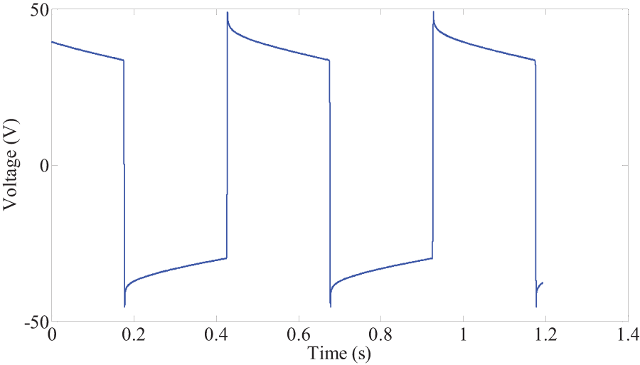
The waveform of the voltage when Vcc = 15 V, and the bypass capacitor is disconnected and the symmetrical switching case is considered.
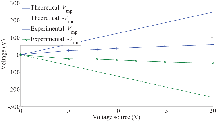
The actuator voltage on the piezoelectric element for the bypass capacitor is disconnected and the symmetrical switching case is considered when the output of the voltage source was increased from 0 to 20 V.
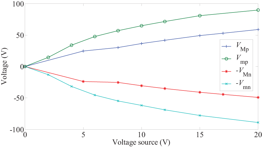
One solution to reduce the influence of the circuit leakage is to increase the capacitance of the piezoelectric actuator. Since the inherent capacitance of the actuator is not easy to change, a parallel capacitor is used to increase the total capacitance. Figure 8 shows the switched voltage when a capacitor of 1.4 μF is connected to the piezoelectric actuator in parallel. The voltage is significantly increased by the parallel capacitor. Figure 8 shows the dependence of VMp, Vmp, VMn, and Vmn on the parallel capacitance when Vcc is 5 V. It is obvious that there is an optimal parallel capacitance, which produces largest voltage on the piezoelectric actuator. This phenomenon is because the quality factor of the switch circuit decreases as the parallel capacitance increases. The optimal capacitance also varies with Vcc. It is about 1.4 μF when Vcc is 5 V as shown in Figure 9.
The switched voltage when a capacitor of 1.4 μF is connected to the piezoelectric actuator in parallel.
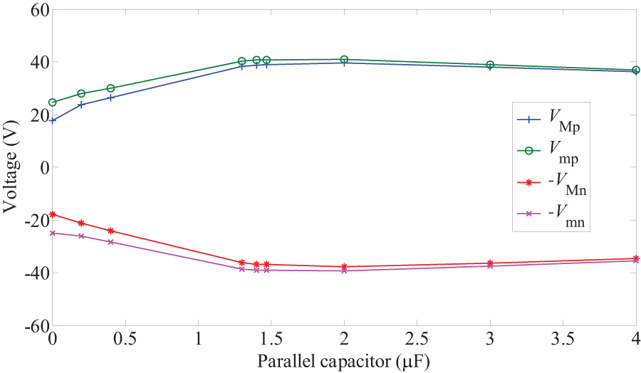
The dependence of VMp, Vmp, VMn, and Vmn on the parallel capacitance when Vcc is 5 V.
Unsymmetrical switching
In unsymmetrical switching, a parallel capacitance of 1.4 μF was connected to reduce the influence of leakage. The waveform of the actuator voltage is shown in Figure 10 when the bypass capacitance is 4 μF and voltage source is Vcc = 5 V. Obvious unsymmetrical voltage was achieved on the actuator. The maximum positive voltage is 53.3 V and the maximum negative voltage is 26.3 V so that the absolute value of the ratio of the maximum voltages is 2.03.
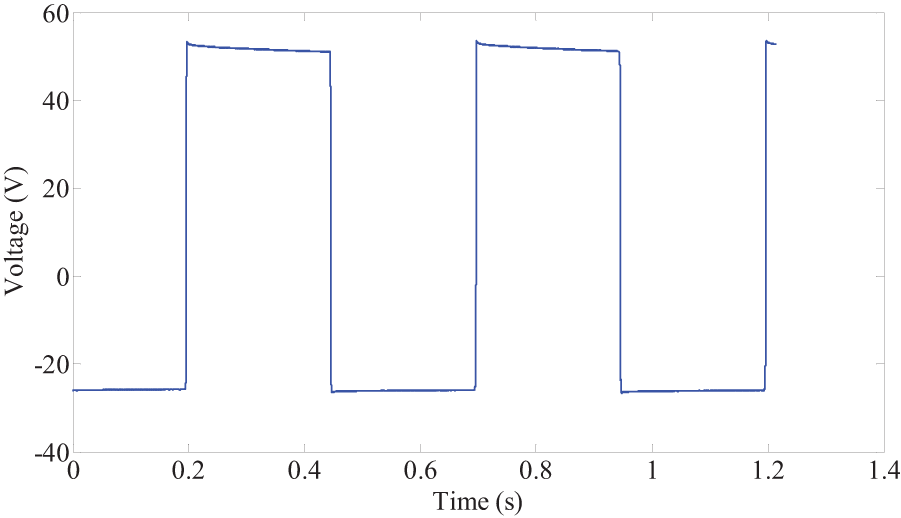
The waveform of the actuator voltage when the bypass capacitance is 4 μF, the bypass capacitance is 4 μF, and the voltage source is Vcc = 5 V.
The theoretical and experimental results of maximum positive and negative voltages are shown in Figure 11 for the bypass capacitance from 0 to 8 μF at an interval of 1 μF, and the voltage source is set to Vcc = 5 V. The theoretical result indicates that the magnitude of positive switched voltage,
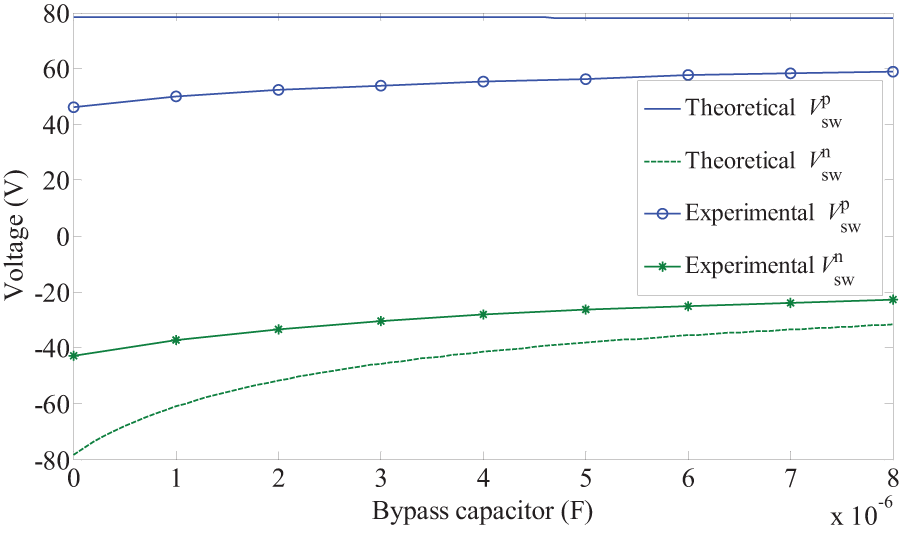
The magnitudes of switched positive and negative voltages for the bypass capacitance from 0 to 8 μF at an interval of 1 μF, and the voltage source is set to Vcc = 5 V.
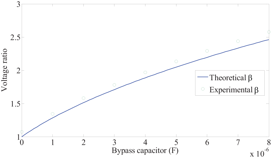
The variation of absolute ratio of the maximum voltages with the bypass capacitance.
Analysis of leakage and improving formulation
Analysis of leakage in the switching circuit
Since the leakage has considerable influence on the maximum voltage on the piezoelectric actuators, it is important to investigate its mechanism. Figure 13(a) shows the decreasing voltage curve of the piezoelectric actuator in the open-circuit state when the bypass capacitance is 1.4 μF. At the beginning, the voltage decreases very fast and the voltage drop can be as large as a few volts. After some time, the voltage decreases almost linearly. In order to modeling this leaking process, the following expression is used to the approximate the time response

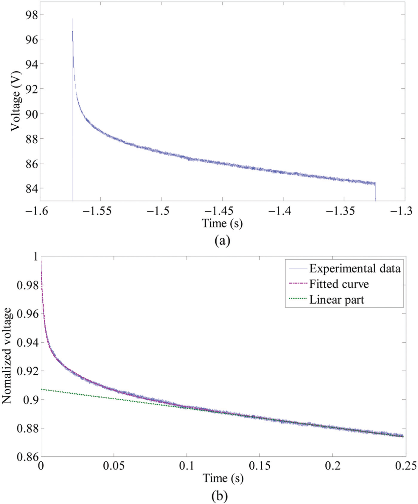
The decreasing voltage curve of the piezoelectric actuator in the open-circuit state when the bypass capacitance is 1.4 μF: (a) actuator voltage at open-circuit state and (b) fitted curve using the proposed model.
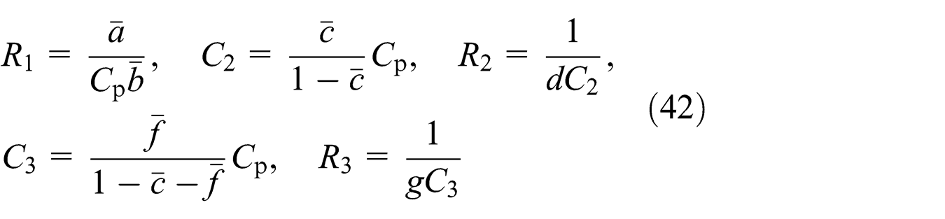
where a, b, c, d, f, and g are the constants to be determined. For convenience, the time is shifted to start from 0 and the voltage is normalized with respect to the voltage at t = 0,
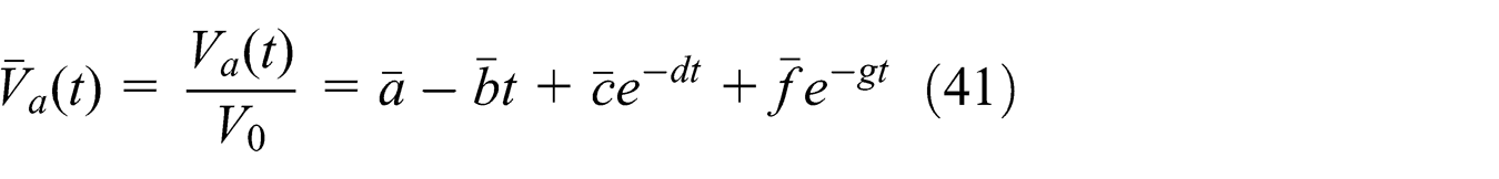
where
Figure 13(b) shows the fitted curved in dash line and its linear part in dash-dot line. Since the fitted line agrees very well with the measured curve, it means that the selected model in equation (41) is a good approximation. The constants
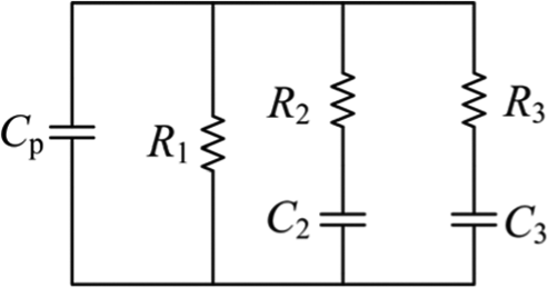
The equivalent circuit in the open-circuit state.
In the above equations, Cp is the total capacitance including the inherent capacitance of the piezoelectric actuator, Cpa, and that of the parallel capacitance, Cpc. That is

The circuit parameters for positive actuator voltage and those for the positive actuator voltage may be different because the positive and negative voltages are blocked by different diodes and MOSFETs, and their electrical characteristics may be different.
In unsymmetrical switching, the bypass capacitor is activated when the actuator voltage is negative. The expressions in equation (42) should be modified to include the bypass capacitor, Cb, as follows
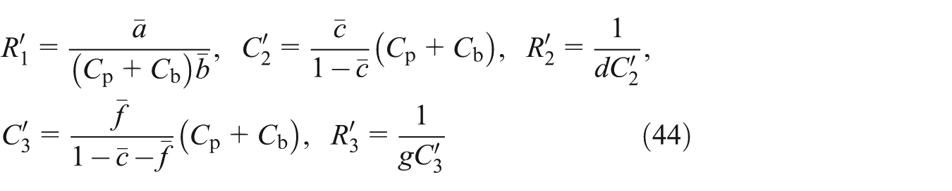
According to the identified constants

The expressions in equations (42) and (44) indicate that if all the circuit parameters are assumed to be constant, independent of the voltage of the piezoelectric actuators, the constant will only depend on Cp and Cb. According to equation (41), the normalized voltage drop depends on Cp, Cb, and the duration of the open-circuit state. The absolute voltage drop will be proportional to the initial voltage
Improving formulation of switched voltage
Because the maximum actuator voltages and the switched voltages calculated from equations (35)–(39) are very different from the experimental results due to leakage of the switch circuit, these equations should be modified to include the voltage drops in the open states. When the voltage drop is considered, equation (34) becomes
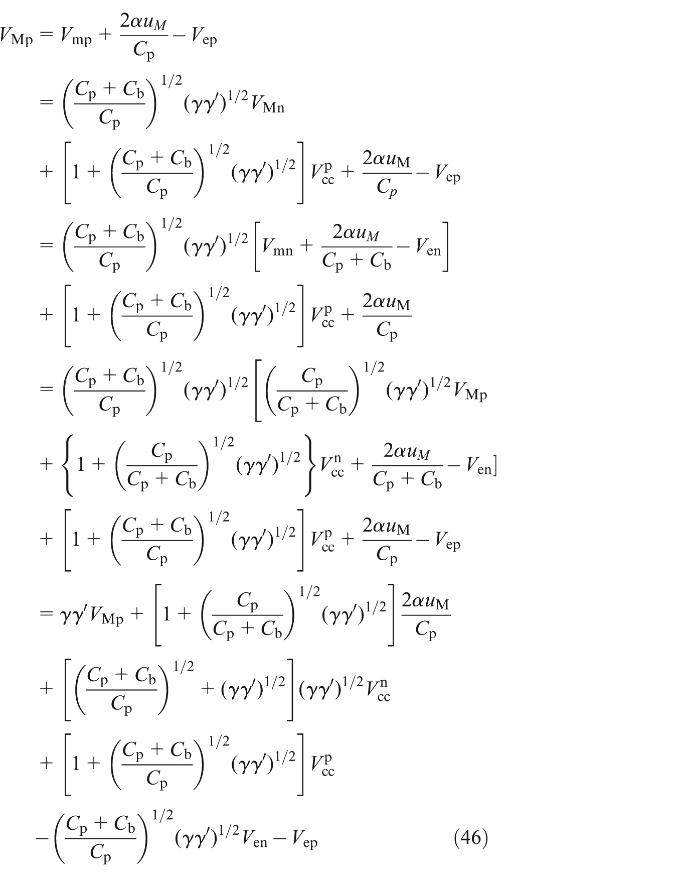
where Vep is the voltage drop due to leakage when the actuator voltage is positive and Ven is the voltage drop due to leakage when the actuator voltage is negative. Solution of
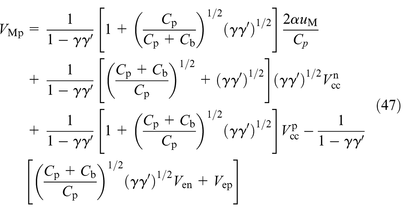
Using the same method, VMn can be obtained
The control effect depends on the switch voltages
and
Using the modified equation, the theoretical results are compared with the experimental results for the symmetrical switching condition with parallel capacitance equal to 1.4 μF in Figure 15. The voltage drops used in the calculation of actuator voltage in equations (47)–(50) are obtained experimentally. Compared with Figure 7, the calculated actuator voltages are better approximations of the experimental results, but there is still large difference between them. A careful investigation of the experimental results indicates that the quality factor of the switch circuit is not constant. As the actuator voltage increases, the equality factor decreases. Hence, the experimental voltages are much smaller than theoretical voltages for the same voltage source. For the unsymmetrical switching with a bypass capacitor of 4 μF, the experimental and theoretical results are shown in Figure 16. Unsymmetrical voltages are obtained on the actuator, but the experimental voltages are much smaller than theoretical voltages, too, in this case. The voltage ratio is about 1.8, which is almost the same for experimental and theoretical results.
Variation of the theoretical and experimental voltages, Vmp and −Vmn, with the output of voltage source, Vcc, in symmetrical switching.
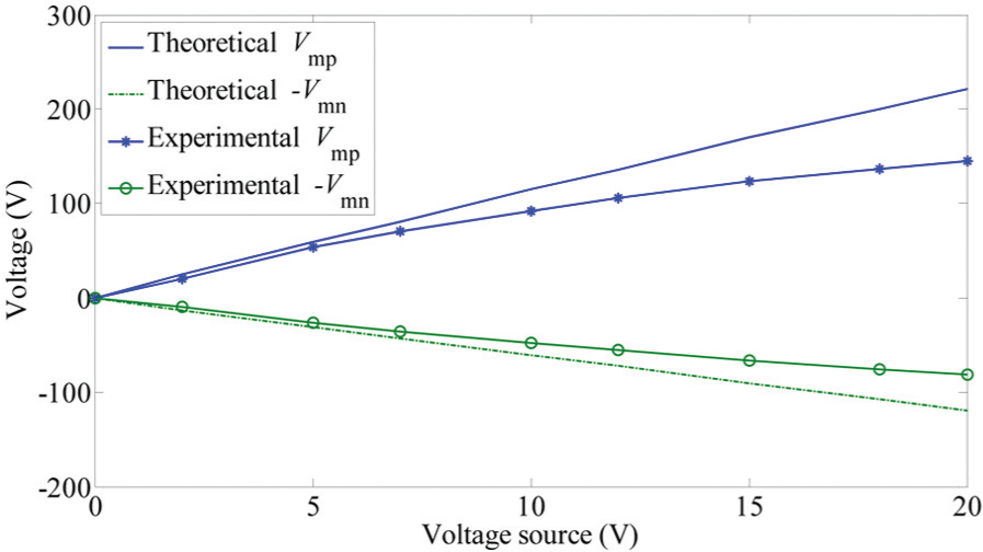
Variation of the theoretical and experimental voltages, Vmp and −Vmn, with the output of voltage source, Vcc, in unsymmetrical switching with a bypass capacitor of 4 μF.
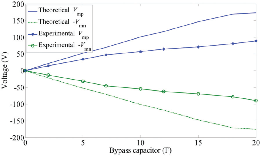
Figure 17 shows the variation of the theoretical and experimental voltages, Vmp and −Vmn, with different bypass capacitances in the unsymmetrical switching circuit, in which the voltage source is Vcc = 5 V. In the calculation, the same voltage drop was used approximately for different bypass capacitances. In the experiments, it was found that the voltage drop changes with the bypass capacitor because it influences the actuator voltage, although the variation is smaller than that in the case of varying voltage source. Compared with Figure 16, the theoretical and experimental voltages are in better agreement. The theoretical and experimental results of voltage ratio of Vmp to Vmn with different bypass capacitances and a voltage source are shown in Figure 18. The relative errors of the voltage ratio calculated from the original equations and those from the modified equations are almost the same, but their direction of deviation is different. The error in the results from the modified equation can be attributed to the approximation of voltage drop used in the calculation.
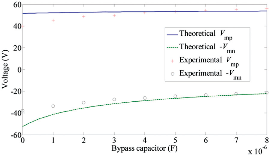
The theoretical and experimental voltages, Vmp and Vmn, with different bypass capacitances and a voltage source Vcc = 5 V in the unsymmetrical switching circuit.
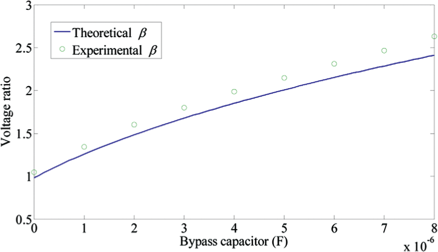
The theoretical and experimental voltage ratio of Vmp to Vmn, with different bypass capacitances and a voltage source Vcc = 5 V in the unsymmetrical switching circuit.
Experimental verification
High-voltage circuit for MFC
A high-voltage unsymmetrical switch circuit was implemented using high-voltage diodes and MOSFETs. The voltage on a MFC actuator bonded to a beam was switched when the beam was fully clamped.Figure 19 shows the switched voltage on the MFC actuator when different voltage sources were used. The parallel capacitance was 1.47 μF and the bypass capacitance was 10 μF. The magnitude of positive voltage was 971 V and the magnitude of negative voltage was 347 V when the output of the voltage source was 105 V. When the output of the voltage was raised to 130 V, the magnitude of positive voltage reached 1150 V and the magnitude of negative voltage reached 410 V. The unsymmetrical voltage ratio was about 2.8. The results indicate that the designed circuit was effective in driving MFC actuators based on the SSDV method.
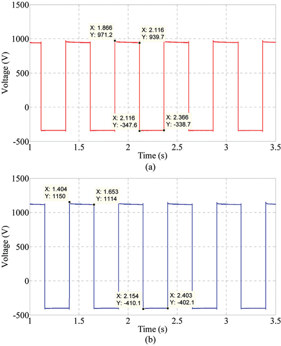
Voltage on the MFC actuator: (a) Vcc = 105 V and (b) Vcc = 130 V.
Control performance of unsymmetrical SSDV
In order to verify the damping performance using the new designed unsymmetrical circuit, an experimental setup of a composite beam bonded with two MFCs is built. One end of the beam is clamped on a mini-shaker which is used to drive the vibration and MFCs are bonded on its surface close to the clamped end. The other end of the beam is free. The beam is 1250 mm long, 76 mm wide, and 1.5 mm thick. It is assumed that the structure acts as pure Euler–Bernoulli beam. In this study, control of the resonant vibration at the second nature frequency of 6.2 Hz is considered.
For comparison purpose, control experiments using both unsymmetrical SSDV and a classical symmetrical SSDV were carried out. The outputs of the positive and negative voltage sources are both 32 V in the unsymmetrical circuit. Figure 20(a) shows the measured displacement of the beam when unsymmetrical SSDV was used. The peak-to-peak amplitude of the voltage on the MFC was 306 V, which ranged from −94 to 212 V. The displacement amplitude of vibration was reduced by 27 dB at the second resonance frequency. However, the first resonance mode was slightly excited. For comparison reason, the output of the voltage sources in the symmetrical switch circuit was set to 33 V so that the voltage on the MFC ranged from −153 to 153 V and the peak-to-peak amplitude was kept at 306 V. The result of classical symmetrical SSDV control is shown in Figure 20(b). Compared with the 27-dB reduction in the unsymmetrical SSDV control, the amplitude of the second mode is reduced only by 16 dB in symmetrical SSDV control.
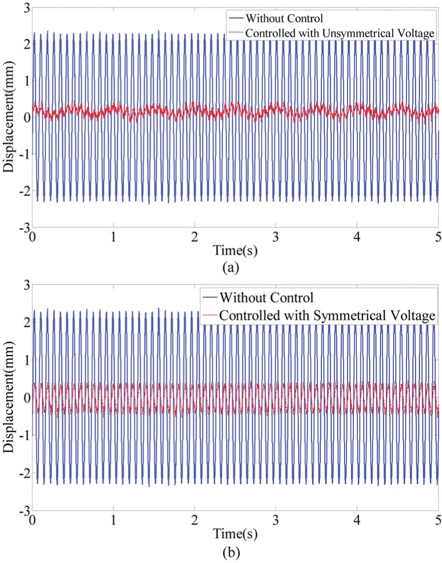
Displacement amplitude of the beam with and without control: (a) unsymmetrical SSDV circuit and (b) symmetrical SSDV circuit.
According to the theory of energy conversion in classical symmetrical switching, the converted energy in a cycle of mechanical vibration is proportional to the peak-to-peak amplitude of the voltage. It indicates that the vibration reduction by the unsymmetrical SSDV and symmetrical SSDV should be the same if the peak-to-peak amplitude of the voltage is the same. The actuator voltage switched at the second resonance mode does not excite the first resonance mode either, according to the classical theory of energy conversion. Hence, the theory of energy converted in unsymmetrical SSDV should further be studied in the future work.
Conclusion and future work
An unsymmetrical switch circuit is designed for the semi-active control method based on synchronized switching damping principle of piezoelectric actuators. A bypass capacitor and an additional switch are used to realize unsymmetrical bipolar voltage. The control logic of the switches is introduced in detail, and the switched voltages, which directly influence the control performance, are derived as functions of the vibration amplitude and the outputs of the voltage sources. The experiments were carried out to verify the designed circuit and the theoretical results of the switched voltage. For simplification of experimental conditions, the beam is fully clamped and the voltage is fully generated by the voltage source. The influence of the voltage source and bypass capacitor on the actuator was investigated theoretically and experimentally. The experimental results show that the circuit leakage is a critical factor to the amplification of actuator voltage. The voltage ratio increases with increasing bypass capacitance, but its increasing rate decreases. The theoretical expression for actuator voltage was modified to include the influence of the circuit leakage. Finally, a working example of the unsymmetrical switch circuit for MFC actuators was presented. The results indicate that the designed circuit was effective in driving MFC actuators based on the SSDV method. The analysis of the converted energy and relationship between the vibration control performance and the unsymmetrical voltage on the piezoelectric actuator will be studied in future work.
Footnotes
Declaration of Conflicting Interests
The authors declared no potential conflicts of interest with respect to the research, authorship, and/or publication of this article.
Funding
The author(s) disclosed receipt of the following financial support for the research, authorship, and/or publication of this article: This research was supported by the National Natural Science Foundation of China under Grant 51375228, Aeronautical Science Fund under Grant 20131552025, Natural Science Foundation of Jiangsu Province under Grant BK20130791, The State Key Laboratory Program under Grant MCMS-0514K01, the NUAA Fundamental Research Funds under Grant NS2013008, and PAPD.