
Abstract
Dielectric elastomer transducers (DETs) are used in various applications, ranging from actuators to sensors and generators. For optimal performance, homogeneous electrical charging characteristics, which depend on the current flow distribution over the electrode area, are indispensable. To enable the investigation of such current flow distributions, a novel approach using thermal imaging (TI) is presented in this paper. The approach uses high-frequency voltage excitation to induce resistive heating in the DET electrodes and generates temperature maps to visualize the current flow, thus providing insight into the local charging behavior. This way, the effects of electrode geometry, electrical contact layout as well as potential manufacturing-related imperfections can be studied. The paper starts by introducing an experimental setup and the effect of excitation parameters. It subsequently illustrates the method using 50 µm strip-shaped silicone films with different screen-printed carbon black/PDMS electrodes, also taking the effect of mechanical strains into account. The results allow for an interpretation of the effectiveness of electrode design, motivate potential future quality tests and may serve as a validation method for, for example, multi-physics finite element simulation tools.
Keywords
Introduction
Dielectric elastomer transducers (DETs) are usable in a variety of applications from sensors (Böse and Ehrlich, 2023; Meyer et al., 2024), over actuators (Hajiesmaili and Clarke, 2021; Mohd Ghazali et al., 2017), to generators (Zanini et al., 2015). Their performance is thereby dependent on their charging characteristics such as charging homogeneity or charging speeds, which in turn are determined by the local current flow over the electrode area. Investigating and understanding the current flow distribution over the electrodes area is therefore indispensable to design and manufacture optimal electrodes for DETs. Addressing this issue, this paper presents a novel experimental characterization approach to visualize and qualitatively characterize the current flow distribution using thermal imaging (TI). The application of a high-frequency excitation voltage leads to resistive heating as a result of the charging- and discharging-related electric current flows. This heat generation can be visualized in two-dimensional thermograms, enabling the identification of temperature fields, which result from an inhomogeneous current flow distribution. Charging characteristics may also influence other DET characteristics, for example, acoustic modes and actuation speeds. In particular for actuator applications such as valves (Xu et al., 2021), pumps (Benouhiba et al., 2025), loudspeakers (Soosani et al., 2020), haptic feedback devices (Son et al., 2023), and for generators (Zanini et al., 2015), charging characteristics are highly relevant. Additional effects, which impact the current behavior can also be identified and characterized. Such effects may include general electrode quality, electrode design, and the design of electrical connections, or the electrical resistance of the DET, which typically falls in the kiloohm range (Wiranata et al., 2021), changes while stretching (Willian et al., 2023) and with the number of operation cycles.
Preliminary results of the experiments shown in Section 4.3 of this article have previously been presented at the SPIE Smart Structures + NDE conference, Vancouver, Canada, 2025 and have been published in the corresponding proceedings (Willian et al., 2025). The current work significantly expands upon these findings by introducing the investigation method in detail and demonstrating its applicability in a number of systematically studied scenarios.
Previously published investigations of the charging characteristics and current flow in DETs have mainly focused on electrical measurements. Studies typically analyzed charge and discharge times (Haroun and Lee, 2022) along with voltage-charging cycles to, for example, optimize generators (Hoffstadt et al., 2013; Zanini et al., 2017). There are also model-based approaches that aim to predict the electrical behavior of DETs, such as lumped-element circuit models or finite element solutions (Rizzello et al., 2020; van Kessel et al., 2021), and coupled thermo-electro-mechanical models (Katzer et al., 2022; Kleo et al., 2020; Vertechy et al., 2013). Also, in other fields of research, such as battery development, the spatial current distribution in planar electrodes has been addressed using analytical models (Taheri et al., 2014). In most cases, these approaches assume homogeneous material properties, idealized interfaces, uniform strain distributions or they neglect edge effects. While such models are well suited to study fundamental mechanisms under controlled conditions, they typically focus on idealized material behavior and therefore address different aspects than the presented experimental approach, which captures real-world influences relevant to DETs, including material defects, strain-dependent localized resistance variations, or electrode inhomogeneities. Consequently, a detailed experimental investigation of the spatial current flow distribution and its sensitivity to various parameters is necessary. However, to the best of authors’ knowledge, such experiments have not been reported in a spatially resolved and electrode-specific manner under AC excitation for DETs. One of the reasons for this is the lack of appropriate experimental methods to study this behavior. Although conventional measurements can provide information on the absolute current flow, they cannot be used to obtain spatially resolved information on the current flow distribution through the electrodes. In addition, optical methods to characterize effects that could influence the current flow in the electrode, for example, inhomogeneous electrodes, cannot be applied to the commonly used carbon-based electrodes due to their black appearance. This work presents a new approach that overcomes previous limitations and complements existing electrical and model-based approaches. It provides a method for experimentally accessing and spatially resolving the resistive heating generated during DET actuation using TI under realistic operating conditions.
TI is an investigation method analyzing the heat radiation which every object emits depending on their radiative properties and temperature (Möllmann and Vollmer, 2007). This technique is used in a variety of other technical fields and covers a wide range of applications such as temperature monitoring in manufacturing processes (Chen et al., 2023), medical applications (Rajmanova et al., 2015), material characterizations (AbouelNour and Gupta, 2023; Lee et al., 2024), as well as various other applications. In the context of electrical systems, TI has been used to detect defects, losses or inhomogeneities, employing various excitation and analysis strategies, such as generating heat by implementing eddy currents (Wu et al., 2019) or electromagnetic induction (He et al., 2018). While these approaches successfully reveal thermal signatures related to defects or losses, they generally address different physical mechanisms and target quantities to those related to the current flow in compliant DET electrodes. In contrast, the approach presented here exploits direct AC excitation of DETs, observing temperature fields due to thermal losses directly associated with the charging and discharging currents in the DET electrodes.
For DETs operating in the high-voltage regime, TI is not an obvious investigation method since electrical currents and power consumption are typically so low that no noticeable resistive heating occurs. Consequently, limited research has been conducted on the use of TI on DETs. Lau et al, for example, used TI to recognize electrical breakdown spots in dielectric elastomer actuators and provide a model for the heating during breakdown (Lau et al., 2016) while Gareis et al investigated and modeled the absolute temperature in the electrical connection points of a DET stack for high frequency applications (Gareis et al., 2022). In contrast to these studies, the presented work focuses on the thermal visualization of the spatial distribution of current induced resistive losses during regular charging and discharging operation of DET electrodes in order to draw conclusions about the current flow distributions. To enable these investigations in the electrodes of DETs it is necessary to adjust the excitation of the DETs. Therefore, a combination of voltage excitation with suitably high frequencies and amplitudes is applied. This leads to sufficient resistive heating over the whole DET area to be measurable with TI, mapping the current paths and current flow distribution in the electrodes. In result, the work provides an experimentally accessible visualization tool for identifying current flow inhomogeneities under realistic operating conditions, which may occur due to different aspects like design of electrical connection, material inhomogeneities or deformation. The generated results will deepen the understanding of DET charging behavior and influences on it, and in future research may be used for training and evaluation of theoretical models of current flow behavior in DETs.
This paper provides a first TI-based study, evaluating its feasibility using carbon black (CB)-based silicone electrodes. CB-silicone is widely used in DET applications (Albuquerque and Shea, 2021; Ashby et al., 2022; Ma et al., 2024), making them a relevant choice for this study, however, the presented method can also be applied to other kinds of DETs using for example, acrylic polymers (Bozlar et al., 2012; Shrestha et al., 2024) as dielectric or other kinds of electrodes such as PEDOT:PSS (Shrestha et al., 2021), carbon grease (Moreno et al., 2024), carbon nanofibers (Yu et al., 2024) and nanotubes (Horii et al., 2023) or metal coatings (Hubertus et al., 2021). As mentioned before, a combination of voltage amplitude and excitation frequency is necessary, which provides sufficient heat generation through resistive heating. Therefore, as a first step, a systematic study is performed to analyze which combinations are suited to conduct such measurements. Afterward, the feasibility of this approach is demonstrated in three use-cases, where different characteristics may influence the current flow over the electrodes area. First, the design of the electrical connection is varied to analyze its influence on the current flow homogeneity. Second, the dependency of the current paths due to inhomogeneities in the electrodes, that is, areas with higher and lower electrical resistance and defects, is shown and visualized. Lastly, the influence of strain on the current paths in the electrodes is displayed, while samples are uniaxially strained up to 100% and thermal images are taken at different strain levels. These investigations are not intended as a comprehensive parametric study but are selected as representative use cases to demonstrate the feasibility of the proposed thermographic investigation approach.
Materials and sample preparation
In the following two sections, the materials (section 2.1) as well as the manufacturing process of DETs (section 2.2) used in this investigation are described.
Materials
The DET compound used as a study object to evaluate the TI-method consists of a silicone dielectric membrane covered with CB filled silicone electrodes. As dielectric, a commercially available silicone membrane (Elastosil Film 2030, produced by Wacker Chemie AG) with a thickness of 50 µm is used. To manufacture the electrodes, Silgel 612 A/B (two component silicone, heat curing, manufactured by Wacker Chemie AG) is used as a matrix material. The matrix material is filled with two CBs, Ketjenblack EC-600JD and Ensaco 350G, while the weight percentages (wt%) of the ingredients in the final prepared electrodes are 77.5 wt% Silgel 612 A/B, 16.88 wt% Ensaco 350G, and 5.63 wt% Ketjenblack EC-600JD.
Sample preparation
Samples are manufactured using the screen-printing process. The silicone membrane is therefore attached to a metal frame. The electrode components are mixed with a planetary mixer and milled with a three-roll mill by EXAKT and the resulting dispersion is used for screen printing. After the electrodes are printed, they are cured in a ventilated oven for 60 min at 150°C. A more detailed explanation of the manufacturing process can be found in prior research (Fasolt et al., 2017; Willian et al., 2024).
The base electrode design consists of a 30 mm × 30 mm active electrode area, electrical connections printed from the same electrode material, and surrounding unprinted silicone membrane resulting in an overall sample size of 50 mm × 50 mm, as shown in Figure 1.
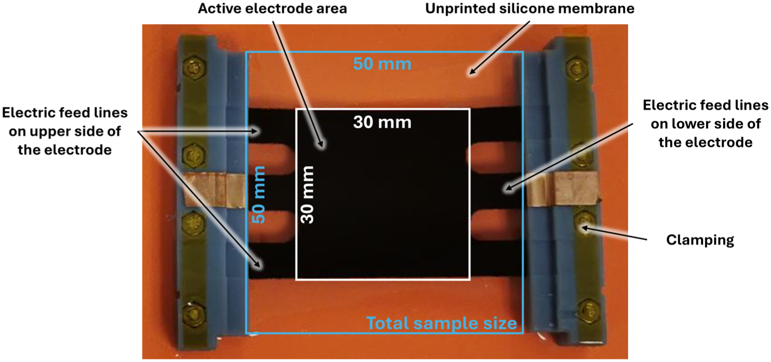
Schematic of a clamped sample with total dimensions of 50 mm × 50 mm while the active electrode area of the DET is 30 mm × 30 mm.
To be able to conduct different investigation scenarios, the active electrode area is combined with several electrical leads allowing different kinds of electrical connection. The chosen contacting system allows different types of contacting to be investigated and their influence on current flow distribution to be examined using the same sample. This enables a direct comparison within one sample of how different contacting designs influence the current flow while minimizing additional influences such as repositioning errors, mechanical handling effects, or sample variations caused by the manufacturing process. The electrode geometry selected is a commonly used in-plane geometry, which can be contacted either on one side or on opposite sides in applications, depending on different factors such as the provided installation space. In Figure 2, a schematic of the printed electrodes is presented, which provides four “arms” for electrical connection at the edges of the active electrode area on the upper side of the dielectric, while there are two “arms” in the middle on the lower side of the dielectric.

Schematic build-up of different layers of the DETs used in this study and additionally all used connection variations used in the tests conducted. Upper half: Top-view on sample with markings of the electrical connections: ① – Upper electrode layer; ② – Active electrode area; ③ – Lower electrode layer; ④ – Dielectric layer; One diagonal: One ground connection in the middle and one high voltage connection on the other side of the sample;  Two diagonal: One ground connection in the middle and two high voltage connections on the other side of the sample;
  One sided: One ground connection in the middle and two high voltage connections on the same side of the sample. Bottom half: Side-view of one sample.
This base geometry is used for all tests conducted. For different investigation scenarios different electrical leads are used.
Test rig and experimental design
In this section, first, a brief description of the test rigs used is provided. Following, the basic investigation method is explained.
Test rig
Figure 3 shows the schematic test buildup of the used test rig.
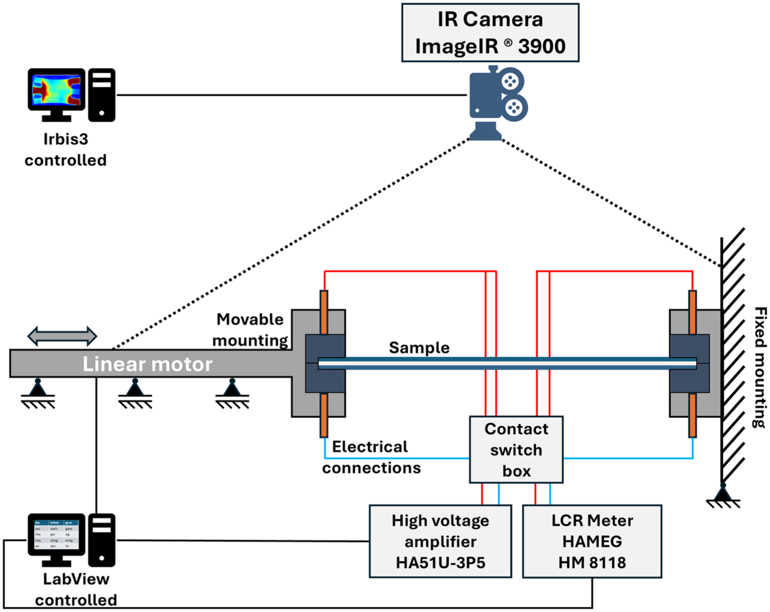
Schematic buildup of the used test rig. Side-view on the sample consisting of one dielectric layer sandwiched between two electrode layers.
The sample is first clamped in 3D-printed parts which allow mounting them into the test-rig. One clamp is fixed, while the other is connected to a linear motor to allow for one-directional straining. Different electrical connection points are available at the clamps to separately allow for variation of the contact points. These connections are integrated into a contact switch box, which allows a fast and easy manual change of the connected cables without interfering with the sample in any way. The high-voltage signal is generated by a HA51U-3P5 high voltage amplifier (hivolt.de GmbH & Co. KG, Hamburg, Germany) which is also connected to a contact switch box. The high voltage amplifier as well as the linear motor are connected to a PC and are controlled via LabView. The infrared-camera (ImageIR® 3900, InfraTec GmbH, Dresden, Germany) is placed above the samples and aligned so that the region of interest covers the range of the unstretched and stretched samples. The camera itself is controlled by a second PC with IRBIS 3 professional software.
Experimental design
TI measures the heat radiation of objects. To be able to measure the temperature of the samples, the IR-Camera is placed over the samples. As mentioned in section 1, the heat radiation of DETs is generally too low for the desired application. To generate a sufficient amount of heat to be detectable with TI, a suitable combination of voltage amplitude
Note that for all ES measurements the cameras’ calibration range is chosen to be −10°C to 60°C, so that the temperature resolution in the region of interest is the highest possible to enable to resolve temperature differences in the samples. In the electrical leads, which are printed out of the same electrode material but do not contribute to the active electrode area, the temperatures in some cases reach temperatures higher than 60°C, but since the investigation of the maximum heating of the samples is not the aim of this work, the absolute temperature values are not discussed. Additionally, it should be noted that the temperatures are not qualitatively analyzed. The tests conducted aim to investigate the current flow distribution in the samples and provide feasibility and showcase the variety of use cases for the presented investigation approach in this article.
Results and discussion
This section presents the results of the preliminary investigation conducted to evaluate favorable
Variation of voltage amplitude and actuation frequency
As discussed above, to investigate the current flow distribution over the samples area enough heat needs to be generated over the electrodes area. Therefore, a systematic study of different
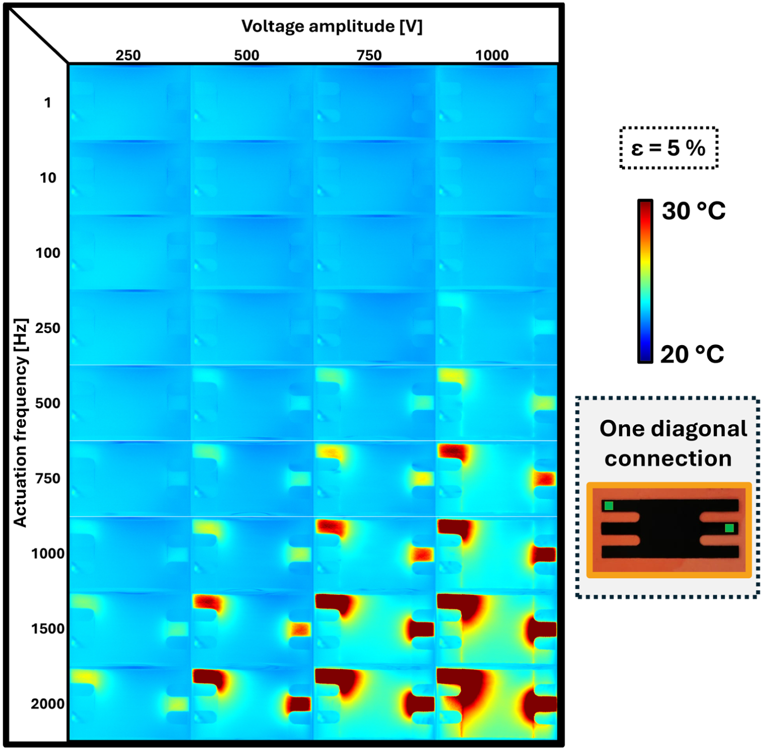
Thermograms for the systematic study with varying
From the thermograms it can be clearly seen that neither a low actuation frequency nor a low voltage amplitude is suited for the desired heat generation. For the sample in Figure 4, an actuation frequency of 1500 or 2000 Hz in combination with a voltage amplitude of 1000 V generates a sufficient amount of resistive heating occurs to heat the whole sample. Therefore, for further tests a combination of an excitation frequency of 2000 Hz combined with an amplitude of 1000 V is chosen. At this point it should be noted that the heat maps show an overlap of heating due to resistive losses and lateral heat flow in the electrodes. This can be seen that is, at an excitation of 1000 V and 2000 Hz. In this case, the temperature of the unconnected connection lines which are close to the connected ones also show a certain temperature increase. This increase is due to lateral heating. When analyzing the thermograms, it is important to be aware of this superposition in order to analyze them correctly. Future work could involve developing models that calculate lateral heat conduction in the samples and distinguish between the two effects for temperature increase. This would enable these effects to be subtracted from each other, providing a clearer view of the heat generated by resistive losses. However, as this article focuses on the feasibility and possibilities of the presented research approach, this issue will not be considered further at this point. Future work must address this issue. Additionally, it should be noted that these combinations are suitable for the presented sample but may differ for other sample designs, which provide other capacities, electrical resistances, or electrode geometries. For the presented ES, these parameters are kept constant as the aim of this work is the general presentation of the novel investigation approach, and to highlight the possibilities it provides combined with the proof of its feasibility.
ES1: Influence of varying electrical connection designs
In this section the TI method is used to characterize current flow distribution and thus charging homogeneity of the DETs in dependency of different electrical connection geometries. Note that the geometries discussed in this section have been chosen to illustrate the effect of different layouts and not for optimization. Additionally, electrodes manufactured for the samples in this chapter have been tailored to show relatively low electrical resistance by printing several electrode layers, thus eliminating influences of defects in the electrodes and concentrating differences on the electrical connection variation. For the measurements conducted in this section, a static strain level of 50% is applied to the samples while the sinusoidal voltage is applied, see Figure 5.
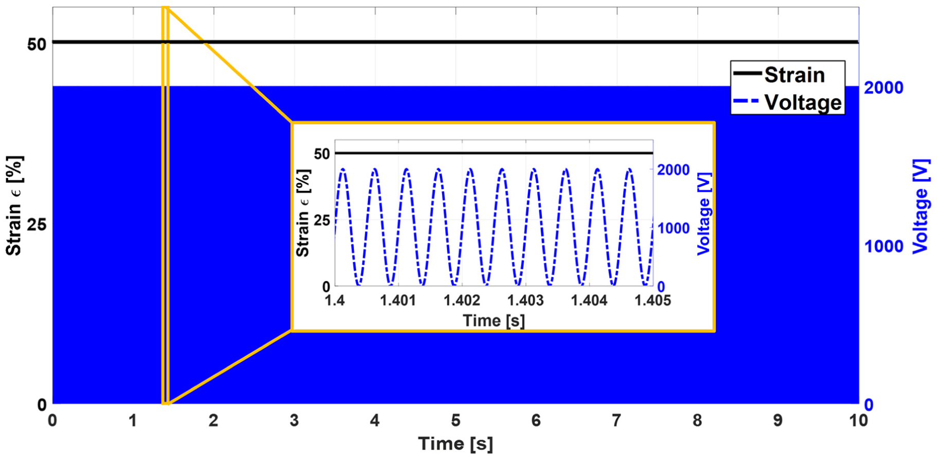
Schematic applied signals to the samples for ES1 and ES2: Constant strain level with simultaneous applied sinusoidal voltage signal.
Thermal images are taken of the samples when they are electrically excited, displayed in Figure 6. Note that the color bar is set to 22°C to 28°C to allow for a detailed inspection of the temperature distribution over the active sample area. The electrical connection area with the peak temperatures is typically clamped and does not actively contribute to mechanical actuation in applications. It should be noted that the electrical connections exhibit different absolute temperatures, depending on the design of the connection. Since these temperatures exceed the upper limit of the selected color scale in all cases, they appear visually similar in the thermograms. As discussed at the end of Section 3, the focus of this work is on demonstrating the feasibility of using this approach to resolve temperature distributions over the active electrode area, rather than on evaluating peak temperatures. The impression of identical temperatures at the connection lines is therefore a visualization artifact caused by the chosen color bar limits.
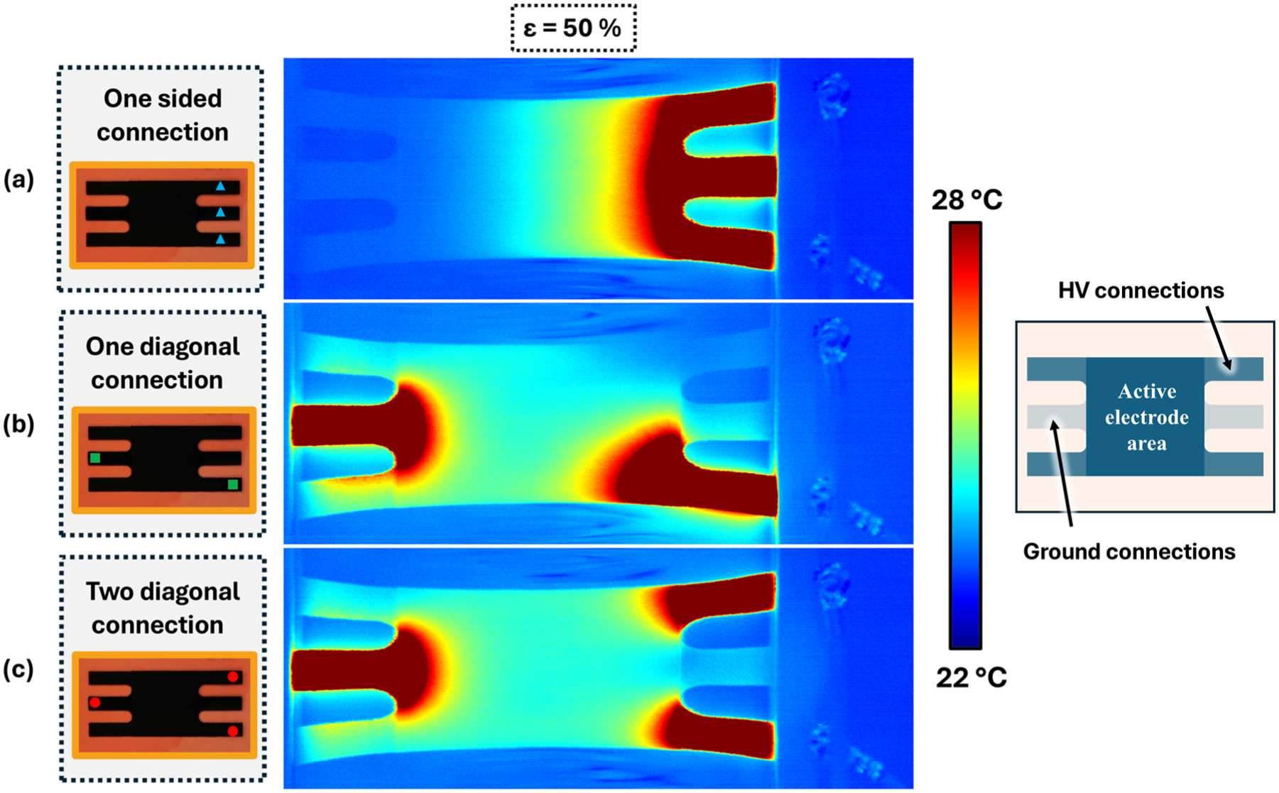
Thermal images of samples with different electrical connection designs, strained to 50% strain: (a) one sided connection, (b) one diagonal contacting, and (c) two diagonal connection; Ground connections are on the lower side of the dielectric and located in the middle at the sides of the active electrode area, while high voltage connections are on the top side of the dielectric and at the corners of the active electrode area.
For the interpretation of the diagrams, it is also important to note that a DET is a capacitive element. Thus – except for a negligible amount of leakage current – the current flow does not occur through the thickness direction of the silicone film, but pre-dominantly within the electrodes on the DET top and bottom surfaces. It is, however, dictated by the electric field buildup which depends strongly on the connection geometry, which differs for the designs in Figure 6 in two main points. First, for Design in Figure 6(a), all connections are placed on the right side of the active electrode area, two high voltage connections at the corner of the sample and the ground connection in between them, but on the opposite side of the dielectric. For designs in Figure 6(b) and (c), the high voltage connections and the ground connections are placed on opposite sides of the active electrode area, resulting in a diagonal connection system. The difference between 6b and 6c is the number of high voltage connections. While for both one ground connection is used on the left side of the sample, on the right side 6b provides one high voltage connection and 6c two high voltage connections, doubling the electrical connection area for the high voltage side. From the thermograms in Figure 6 one can directly conclude that the electrical connection has a strong impact on the current flow in the electrodes. For all cases, the heating is most pronounced in the electric connection arms and close to the contact regions. Imaging the charge flow onto and from the electrodes, all charges need to go through the connected arms, thus concentrating on the current flow and therefore the resistive heating in those arms. After the charges pass the connection arm, they distribute over the sample. As a result, the temperature generated by resistive heating decreases over the sample area. This can easily be seen for the “one sided” connection in Figure 6(a). As all connections are on one side of the sample, the temperature is the highest on the right but decreases gradually from the connected side of the sample to the unconnected side, until the sample has nearly ambient temperature (∼22°C), since there no noticeable thermal heating occurs. A high concentration of temperature increase is unfavorable as this alters DET characteristics such as the stress-strain behavior (Porte et al., 2024) or the dielectric constant (Sheng et al., 2013). By designing electrodes in a way that the contact region increases, or that the current flow into the electrodes is more distributed, such temperature increase can be reduced, leading to less influence on the DET properties. This can be seen in Figure 6(b), when the sample is connected in the “one diagonal” connection. The temperature increase is more distributed over the electrode, which provides a more homogeneous thermogram, indicating a more homogeneous charging characteristic. However, it can be seen that the contact regions still provide a wide area with high temperatures. Additionally, in the upper right corner no noticeable heating occurs, as the current flow distribution is still inhomogeneous due to this type of connection. When the number of high voltage connection arms is doubled for the high voltage side in Figure 6(c), the charging homogeneity increases. This can be seen as in comparison to Figure 6(b), the sample temperature is more homogeneous. Also, the contact regions provide a lower area of high temperatures, as the charges can spread more evenly over the sample and have double the connection area, reducing the charge flow concentration in the contact region. This leads to a more homogeneous electrical field over the sample area.
This ES confirms that optimized contact design remains essential for minimizing thermal stress, especially under dynamic conditions. With the presented method, the current paths in dependency of the electrical connection could be made visible, as well as the general homogeneity of charging in dependence of the design of the electrical connection. Such measurements can help to understand charging characteristics and the actuation behavior in dependency of the current paths in DETs. Additionally, it can help to improve and optimize the design of the electrical connection to achieve the desired charging and actuating characteristics, reducing thermal stresses and potential negative effects on the DET characteristics or their fatigue behavior.
ES2: Implemented inhomogeneities
In ES2 the feasibility of the detection of imperfections with the presented method is to be verified. To detect imperfections, it is necessary to analyze the change in current flow due to the change in electrical resistance because of defects. To achieve this goal samples with implanted defects are prepared as shown in Figure 7.
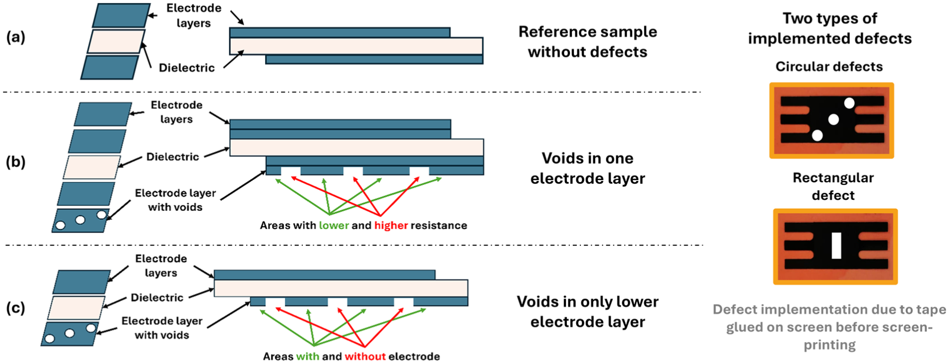
(a) Schematic illustration of a reference sample without defects, (b) schematic illustration of a sample with three voids as implemented defects in one of the electrode layers, thus creating regions with different electrical resistances, and (c) schematic illustration of a sample with three voids as implemented defects in the lower electrode layer, thus creating actual holes in the final electrode; On the right: Schematic visualization of the implemented defects in the samples. Reproduced and adapted with permission from Willian et al. (2025).
Figure 7(a) displays a reference sample without any imperfections. In comparison to this a sample with locally varying electrode thicknesses is manufactured as displayed in Figure 7(b). To achieve this, two electrode layers are printed on each side of the dielectric. By applying tape pieces to the screen, as schematically shown in Figure 7 on the right side, the mesh was covered at specific spots when the second electrode layer of the lower electrode was printed. Therefore, the lower electrode provides areas with different electrode thicknesses and thus with lower and higher electrical resistance (Fasolt et al., 2017). A third kind of sample is manufactured, as it is shown in Figure 7(c), with only one electrode layer on each side while the lower electrode layer contains holes. Samples which contain actual holes in the lower electrode layer, as displayed in Figure 7(c), provide defects with the same geometrical dimensions, but in the strongest expression, namely as voids, where electrode areas are not connected to the rest of the electrode. These samples are intended to demonstrate that not only imperfections can be detected with the examination method presented, but also that the intensity of such can be determined qualitatively. To be able to distinguish defects, samples without implemented defects are measured as reference. The implemented inhomogeneities represent inhomogeneities or defects, which for example, may occur during manufacturing by using worn tools or a not optimized manufacturing processes, or due to fatigue behavior of the electrodes.
For the investigations conducted in this section, samples are strained to 50% and then the sinusoidal voltage signal is applied, providing the same test procedure as shown in Figure 5. The resulting thermal images of a defect free sample as reference and samples with circular inhomogeneities are shown in Figure 8.
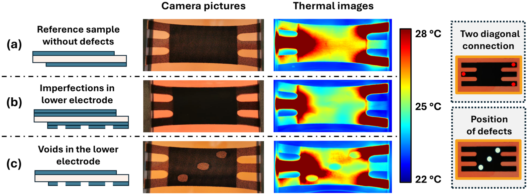
(a) A defect free sample as reference, (b) a sample with varying electrode thickness in the lower electrode, and (c) a sample with voids in the lower electrode; First column: Photographs of the samples; Second column: Thermograms of the samples. Reused with permission from Willian et al. (2025).
Starting with the reference sample in Figure 8(a), as expected from an inhomogeneity free sample, no anomalies can be distinguished in the camera picture. The resulting thermogram then provides symmetric heating behavior, while heating is more pronounced at the connection points than on the sample area. The heat fronts from the contacts look therefore roundish, as the temperature decreases from the contacts to the middle of the sample. Note that, in comparison to the sample in Figure 6, here the sample provides higher electrical resistances, thus providing higher thermal losses and therefore a different thermogram, which shows higher temperatures but the same heat map structure. Similar to the reference, also in the camera picture of the sample with areas of higher and lower electrical resistance in Figure 8(b), no anomalies can be detected. This is due to the black appearance of the CB-silicone electrode. Nevertheless, when the voltage signal is applied and a thermogram is taken from the sample, differences to the reference sample can be distinguished. If compared to the schematic visualization of the position of defects on the right in Figure 8, it can be seen that the heating is less pronounced in the areas of the inhomogeneities, where a higher electrical resistance is present. The current flow avoids these areas and rather flows around them, resulting in higher heating around the imperfections. This phenomenon is more expressed in the samples with actual holes in the lower electrode. While in this case, also these spots can be seen in the camera picture, these may resemble areas which lost complete contact with the surrounding for example, due to filler agglomeration or due to fatigue mechanisms. Such effects would most likely not be visible with camera pictures but can be made visible with TI. The current needs to flow around these holes without electrodes, resulting in an even higher heating in the surroundings. The shape of the heat distribution is thereby similar to the one of the samples in Figure 8(b), but in a stronger expression. This highlights that with this approach, not only can the presence of inhomogeneities be visualized, but qualitative also severity.
As discussed, samples with a rectangular inhomogeneity are also prepared. Next to a reference sample a sample with a rectangular inhomogeneity providing areas with higher and lower electrical resistance is investigated. Next to this, another sample with a different defect is presented. As mentioned in Figure 7, the defective samples have been prepared by applying glue tape to the screen. While printing the samples with the rectangular defects, some of the printing material was pressed under the edges of the tape. The solvent contained caused the adhesive to separate from the tape and enter the mesh. This resulted in a fine line of clogged meshes in the screen. Further printing with this screen resulted therefore in defective lines in the electrodes, as no electrode material could pass the clogged mesh. These lines are in width lower than 100 µm and are not visible with the pure eye. Figure 9 displays thermograms of a reference sample, a sample with a rectangular inhomogeneity providing areas with higher and lower electrical resistance, as well as a sample, which has line defects due to a clogged screen.
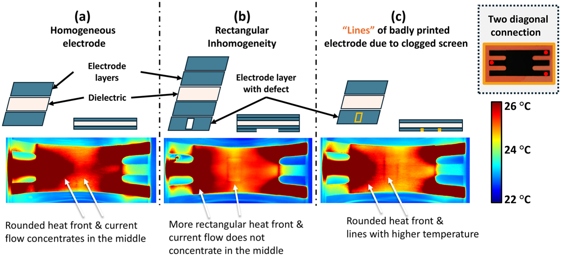
(a) Thermogram of a sample without defects as reference, (b) Thermogram of a sample with a rectangular hole in the lower electrode layer, and (c) Thermogram of a sample with defective lines from a clogged screen. Reused with permission from Willian et al. (2025).
The reference sample shows symmetric heating behavior, while the sample with the inhomogeneity provides a different heat front. While the heat front at the connection of the ground electrode (left side) for the reference is roundish, for the sample in Figure 9(b) it becomes more rectangular. This is because the current avoids flowing through the middle of the sample, as the rectangular inhomogeneity provides higher electrical resistance. Therefore, the preferred current flow regions in 9b are trending more to the sides of the sample. This behavior is similar to the circular inhomogeneities in Figure 8. In the thermogram in Figure 9(c) for the sample, which was prepared with a clogged screen, these line defects are also visible. At these lines the measured temperatures are higher than their surroundings. It is assumed that this is because corner effects leading to increased electric fields at these lines, but this phenomenon needs to be further investigated. Nevertheless, also these smaller defects can be detected.
The measurements conducted in ES2 show that imperfections and defects in the DET electrodes can be distinguished with this investigation approach with TI, while they are not visible with other optical methods like normal camera pictures as shown in Figure 7. Next to the feasibility of this measurement method for detecting imperfections, ES2 also proves that the thermograms of the samples show the current path distribution in the electrodes and that the heat flow from the hotter leads is not the dominant factor for the samples’ areal heating. This finding is a decisive basis for the general usability of this method, not only for the investigations carried out in ES2, but also for ES1, ES3, and other potential areas of application. Being able to visualize defects and imperfections in the electrodes could be used in various applications such as quality controls of the electrodes after manufacturing or investigating samples after fatigue tests. This could be automated by training models and algorithms which detect variations with respect to reference samples and thus also quantify what kind of defect is present in the sample.
ES3: Effect of uniaxial strain
In ES3 the feasibility of the presented measurement method to analyze current path changes in the electrodes as a function of strain is evaluated. By straining DETs, their electrical resistance changes. The measurements conducted with the presented investigation approach aim to highlight the possibility of the visualization of the current flow and its change due to strain. With occurring necking, the strain distribution over the samples is more complex, leading most probably to locally differing electrical resistances, thus influencing the current flow in the electrodes. Visualizing the current paths and their changes while stretching therefore can be used to make qualitative statements about the local differing electrical resistance and could be used to improve and optimize the electrodes in the future to generate a desired behavior. To achieve this goal the samples are stretched cyclically at 0.05 Hz between 0% and 100% strain while the sinusoidal electrical excitation is applied simultaneously, as schematically shown in Figure 10.
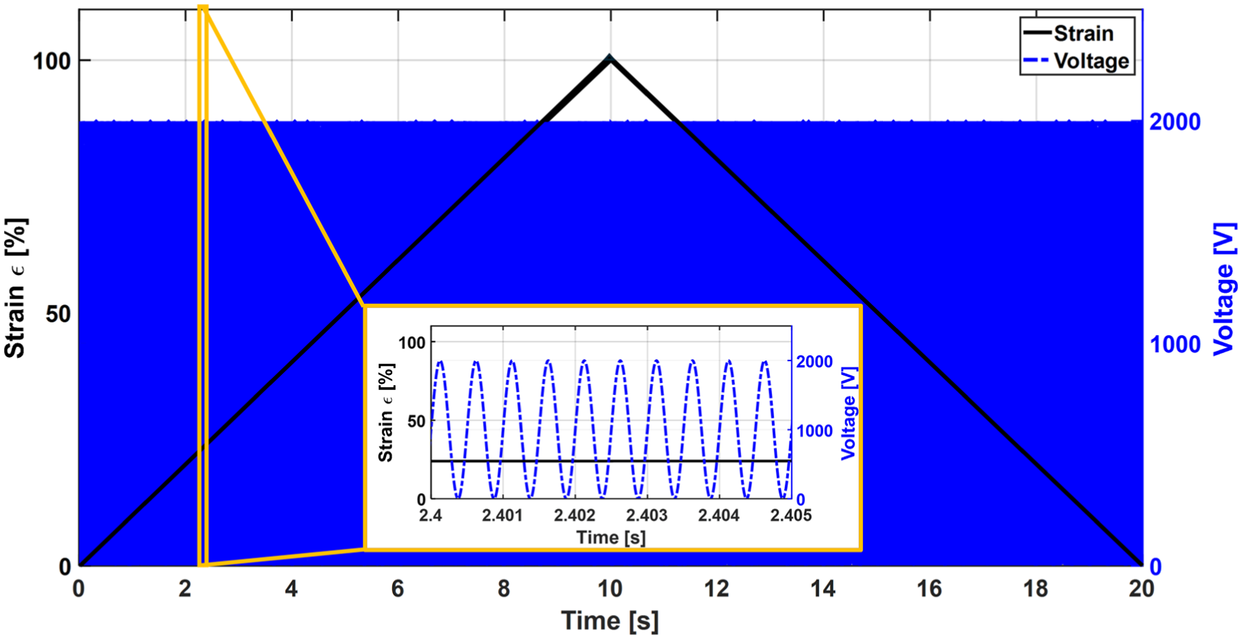
Schematic applied signals to the samples for ES3: Triangular applied strain level with simultaneous applied sinusoidal voltage signal.
The thermograms of a sample which is one sided connected and one which is one diagonal connected are shown in Figure 11.
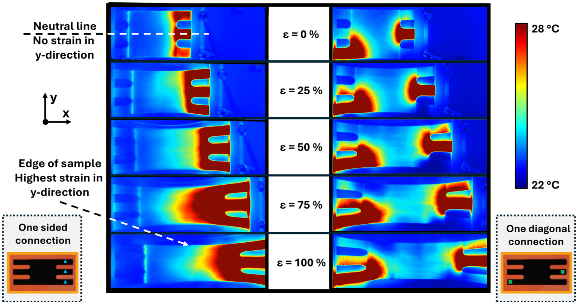
Change in heat distribution over the sample due to straining to ε = 100%; On the left a sample, which is connected on one side; On the right a sample, which is connected one diagonally.
Thermal images have been shot for different strain levels, between 0% and 100% strain in 25% steps. At lower strain levels until 50% the temperature gradient distributes evenly over the sample from the point of connection. For 75% and 100% strain, the shape changes significantly. For the one-sided connected sample, the thermal front becomes more roundish, which means that in the middle line of the sample, the “neutral line” as marked in Figure 11, more resistive heating occurs than at the free edges of the sample on the upper and lower side, marked also in Figure 11. Similar behavior can be seen for the one diagonal connected sample, while the heat generation is more pronounced in the neutral line at higher strains. This indicates that for lower strains, the current flow is more homogeneously distributed over the sample. In this region, strain dependent changes in the sample are more homogeneous. Thus, the electrical resistance in the sample does not significantly differ locally over the sample area. For higher strain levels, this changes because the local strain distribution in the specimens becomes more inhomogeneous as effects like necking become more pronounced. In this strain region, the current concentrates in the neutral line of the sample. This can be due to differing electrical resistances in the electrode while stretching. In the initial state, the electrode resistance is homogenously over the whole sample. When stretching, the resistance of the electrode changes. For such systems, an increasing electrical resistance with increasing elongation of the electrodes is a known phenomenon (Danner et al., 2022; Rosset and Shea, 2013). Usually, the resistance change for DET electrodes is considered homogenous over the electrode area or it is not discussed in other research, as a direct investigation of the local resistance distribution is not easily practicable. However, using the presented measurement method it is possible to visualize the current flow distribution due to local differences in the electrodes. The higher current flow and therefore heating in the middle of the sample implies that the electrical resistance change is lower in the middle of the sample than at the edges of the electrode. This could be explained due to the necking of the samples. In strain direction, the sample is strained up to 100%. Nevertheless, the neutral line in strain direction does not undergo any strains perpendicular to it. The further away from that line of zero perpendicular strain, the higher the localized strain in y-direction becomes. Since for such systems a higher strain leads to higher resistance, the increased strain at the edges is most likely responsible for resistance differences in the sample, thus the current flows through the lower resistive areas in the middle line of the sample. While for the investigated case, this is only of interest for strains above 50%, this might be of higher interest for different electrode geometries, for example, geometries which show stronger necking behavior or samples with differing dimensions, also potentially at lower strain levels. Especially for electrodes, which are susceptible to strain influences, for example, metal electrodes which show cracking behavior when they are strained, this investigation method can help to visualize the current flow distribution and thus draw conclusions on the resistance behavior. Additionally, this method may be employed in fatigue testing to monitor changes in current flow distribution over several million cycles or extended periods, thereby providing insights into resistance evolution due to material fatigue.
It could be shown in ES3 that the current flow in dependency of the strain can be visualized with TI, which is not practicable with other investigation methods. This proves the feasibility of such measurements with TI. With this, it is possible to characterize how current distribution changes depending on the strain level and therefore characterizes the DET behavior in a new way. It may help to understand the resistance behavior of DET electrodes in the future and may help to design electrodes and their connection such as the current flow is more homogenous over the DET area also at higher strains.
Conclusion
This article introduces a novel approach for the characterization of DETs using TI and demonstrates its feasibility through three experimental series (ES). By applying sinusoidal electrical excitation with a high voltage amplifier, temperature increase is generated through resistive heating. This heat generation is most pronounced in regions with the highest local current flow. In result, the heat maps of the samples represent the two-dimensional current distribution in the samples. With this method, the current flow over the electrode can be visualized, which is not practicable with other optical methods. The experiments conducted illustrate and evaluate different use cases of the measurement approach, giving an initial overview of its application potential. This aim is achieved by three different ES. In ES1, samples with different electrical connections but same active electrode area and design are investigated. With TI it could be shown how the current flows depend on the design of electrical connection. The current flow is more homogeneous over the electrode area when the cross-sectional area of the contacts increases, lowering the overall electrical resistances, and thus showing lower measured temperatures. Such measurements can help to identify suitable electrical connections to achieve more homogeneous charging behavior and reduce thermal stresses, which potentially alter DET behavior and fatigue behavior. In ES2 samples with implemented inhomogeneities are examined. Areas with higher electrical resistance and voids in the electrodes are introduced in the samples and their influence on the current flow distribution is investigated. With TI, it was shown that the current flow is significantly dependent on these inhomogeneities. The inhomogeneities could be visualized in comparison to a reference sample, as the current flow avoids these areas, resulting in higher heating in the surroundings. Being able to visualize this effect can be useful for different aspects such as quality control of the electrodes after manufacturing or characterization of degradation processes in long-term fatigue tests, that is, that inhomogeneous deformations could lead to locally differing aging effects. Lastly, in ES3 the samples are stretched cyclically between 0% and 100% and simultaneously electrically excited, while heat maps were captured in 25% strain steps. In the measurements it could be shown that, while homogeneous over the electrode area at low strains, the current flow concentrates in the middle of the sample at strains higher than 50%. This might be due to locally different changing electrical resistance for example, because of necking. This provides a more detailed investigation into the electrode resistance change depending on the applied mechanical strain. It could also help to design electrodes such as, when stretched, a more homogeneous electrode behavior is achieved. The results of this work demonstrate the feasibility of the presented approach and illustrate their importance, providing the reader with a first impression of the possibilities this kind of investigation has for future DET characterization. Being able to characterize such effects will allow a further improvement of electrodes regarding their design, manufacturing, charging characteristics, high frequency behavior, and fatigue behavior to achieve optimal performances.
However, for a novel measurement and characterization approach, there are also aspects and limitations to be considered. Depending on the desired property to be analyzed, the excitation should be chosen to avoid triggering oscillating modes that are not the subject of the investigation. The applied voltage should be as low as possible to prevent actuation and to minimize sample movement and thus sample cooling and acoustic modes. This should always be done in combination with a suited excitation frequency so that sufficient heat is generated to perform the measurement. Simultaneously the heat generation should be as low as possible, so that the temperature increase in the contact points does not distort the thermal images due to heat conduction. It should always be remembered that the heat map obtained is a superposition of the heating of the two electrodes of the DET. Post-processing is an essential aspect for the applicability of this characterization method. The choice of suitable color bar limits is indispensable, since incorrectly chosen limits may hide effects that can be seen with other boundaries. This problem might be avoided for example, in combination with artificial intelligence, which iterates automatically through color bar limits and compares the thermograms with references. Further research will need to take these aspects into account in order to ensure that the measurement methods presented are reliable and useful in future investigations.
In summary, characterizing the local temperature increase through resistive heating and visualizing it with TI provides a new approach to characterize DETs. The use of this method is not restricted to the examples in this article. Combining TI with other measurements methods, for example, vibrometers to analyze the influence of electrical connections on the formation of acoustic modes, may lead to even deeper understanding of DET behavior. Also, an expansion of the conducted measurements on other electrode designs, other actuator designs, for example, rolled, circular out of plane, or layered DETs, or other electrode materials such as metal coatings is possible. The results may also be used as a basis for future modeling approaches to predict the localized current flow distributions in DETs.
Footnotes
Acknowledgements
The authors would like to express their gratitude to Wacker Chemia AG for providing Elastosil 2030 50 µm silicone membrane for preparing the DETs examined in this work.
Funding
The authors received no financial support for the research, authorship, and/or publication of this article.
Declaration of conflicting interests
The authors declared the following potential conflicts of interest with respect to the research, authorship, and/or publication of this article: One of the co-authors of this manuscript, Stefan Seelecke, is serving as a Guest Editor for the special issue to which this paper has been submitted. To avoid any potential conflict of interest, Stefan Seelecke has not been involved in the editorial handling or peer review of this manuscript.
Data availability statement
The data that support the findings of this study are available from the corresponding author upon reasonable request.*