






Abstract
Dislocations and dislocation dynamics are the cores of material plasticity. In this work, the electric features of dislocations were investigated theoretically. An intrinsic electric field around a single dislocation was revealed. In addition to the well-known Peach–Koehler force, it was established that an important intrinsic electric force exists between dislocations, which is uncovered here for the first time and has been neglected since the discovery of dislocations. The electric forces may be large and sometimes could exceed the Peach–Koehler force for metals and some dielectric materials with large dielectric constant. Therefore, the electric force is anticipated to play a vital role in dislocation dynamics and material plasticity. Moreover, an external electric field could exert an electric force on dislocations and a threshold electric field was subsequently discovered above which this force enables dislocations to glide. Interestingly, it was found that some dislocations move in one direction, but others move in reverse in an identical electric field, which is in agreement with experimental observations. Despite dislocation motion under an electric field, to one’s surprise, both edge and screw dislocations do not carry net charges by themselves, which may tackle the long-standing puzzle on the charges of dislocations. These findings may supply people with new fundamental knowledge on dislocations as well as dislocation dynamics, and may assist people in understanding related phenomena.
1. Introduction
Dislocations are a primary crystalline plastic mechanism and dominate plastic behaviors of crystalline materials. These dislocations have been found to display both mechanical and electric features. In addition to mechanical properties, electric features of dislocations are interesting and important, which has been indicated by the related investigations. To explore the electric properties of dislocations, several experimental methods have been developed and utilized, for example, dislocation motion driven by an externally applied electric field [1], electron-beam-induced current (EBIC) of dislocations [2, 3], electrical conductivity of nano-contact semiconductor wafer with dislocations [4], electrical conductivity of dislocation-stored thin films [5], electrical voltage during dislocation-based plastic deformations [6], motion of low-angle grain boundaries constructed by edge dislocations under an external electric field [7], and so on.
Based on these experimental methods, dislocations were found to present intriguing electric properties. The existence of dislocations usually detrimentally reduces the function of semiconductor-based devices [8], indicating that understanding the electric properties of dislocations is the key to the next-generation nano-devices. The majority of dislocations in pure crystal NaCl was experimentally observed to move opposite to the electric field, demonstrating that they are negatively charged [1]; however, a large proportion of dislocations was indeed found to move along the electric field, which was disturbing [1]. The application of a strong electric field enables dislocations to glide in bent LiF crystals [9], which was attributed to positively charged dislocations [9]. Experimental observations indicated that the dislocations are negatively charged in LiF and NaCl crystals [10]. Experimental results for single-crystal NaCl showed that negative charges appears on the concave side, whereas positive charges emerges on the convex sides [6], and only the edge dislocation components correlates with electrical charges [6]. The pure tilt low-angle boundary motion was observed under a threshold electric field, and the driving force for the boundary motion arises from the interaction between the electric field and the array of charged edge dislocations [7]. Experiments showed that for a single-crystal NaCl plastically deformed in an inhomogeneous manner, an electrical current flows through the crystal, suggesting that the dislocations must be positively charged [11]. It was indicated in experiments that edge dislocations carry negative charges in a nominally pure crystal NaCl but bear positive charges in an oxide-doped crystal [12]. Unlike edge dislocations, screw dislocations were not detected to exhibit charge effects [12]. In the vicinity of room temperature, dislocations in single-crystal NaCl were positively charged [13]. By means of dislocation photoconduction spectrum in alkali halide crystals, a strong internal electric field around an edge dislocation was established in ionic crystals such as NaCl, KCl, KBr, and KI crystals [14]. In a single-crystal KCl doped with CaCl2, experimental observations showed that only edge dislocations can be driven by a large electric field and they are negatively charged [15]. In addition, in Ca2+-doped single-crystal KCl, only when an electric field is larger than a critical value can the edge dislocations be moved [16], and the charges carried by dislocations is initially negative but can change from negative to positive [16]. Both experimental and theoretical studies on charged dislocations in alkali halide crystals were reviewed [17], phenomenological models for charged dislocations were discussed [17]. In a review [18], it was shown that movement of dislocations may lead to the electric effects accompanying plastic deformations and the electric signals was ascribed to the motion of dislocations bearing electric charges. Experimental observations on electroplasticity showed that when mechanical plasticity happens for a material, flow stress is usually reduced noticeably by an applied electric field [19]. It was attributed to enhanced dislocation mobility, which arises from an electric field applying a driving force on dislocations [20]. Experimental investigations on charge effects of dislocations in ionic crystals revealed that charges carried by dislocations may depend on temperature and impurities [21]. Upon sign of charges possessed by dislocations, many of the experimental results, even in the same type of crystals, were still heavily debated [21].
Theoretical effort has also been spent to clarify the related phenomena. Electric interaction between a dislocation and a solute atom was considered in copper-based alloys, and calculations suggested that it is between 1/3 and 1/6 of the corresponding elastic interaction [22]. The electric field effect on the movement of edge dislocations in smectic layers was discussed [23]. For a one-dimensional quasicrystal, the electric–elastic field caused by a straight dislocation was addressed [24]. For some piezoelectric semiconductors and ceramic materials, a charged three-dimensional dislocation loop model was developed for novel layered structures [25].
As mentioned previously, despite the many experimental and theoretical attempts having been made to clarify the electric features of dislocations, the underlying physical origin is still puzzling.
In the other respect, the interaction between dislocations is also of paramount importance and it usually plays a pivotal role in dislocation dynamics, as indicated by numerous studies. Edge dislocations were found to accumulate to form sub-boundaries by means of dislocation interaction [26]. Interaction between dislocations was employed to study the dislocation spacing dependence of external shear stress that can drive them to intersect [27]. Interaction between screw dislocations and grain boundary edge dislocations was employed to understand impediment of dislocation gliding across low-angle grain boundaries [28]. The mutual interaction between dislocations in two-dimensional colloidal crystals was investigated by means of video microscopy analysis on particle trajectories [29]. Pair interaction of nearest-neighbor dislocations was found to cause a tail distribution of the dislocation velocity in a form of power law [30]. Discrete dislocation dynamics (DDD) simulation was carried out to analyze transport of dislocations underneath a sliding contact with a tip in some crystals [31]. During indentation and sliding, DDD was performed to study frictional properties of contact [32, 33]. A three-dimensional phase field dislocation dynamics (PFDD) model was utilized to explore the relationship between the Peierls barrier and line characters of dislocations [34]. Two-dimensional DDD simulations were used to elucidate the nano-indentation properties of a single crystal [35]. A geometrically projected DDD was proposed to simulate dislocation motions under high strains and long time scales [36]. Three-dimensional DDD was utilized to delve into the nano-indentation behaviors affected by grain boundaries for an aluminum bicrystal [37]. Based on DDD, dominant yielding mechanisms in single-crystalline copper nano-pillars was investigated [38], and for dislocation nucleation mechanism a transition from dislocation multiplication to surface nucleation was observed [38]. Two-dimensional DDD simulations were performed to minimally capture the phenomenology of nanocrystalline deformation [39]. In terms of three-dimensional DDD, screw dislocations were found to have an important effect on strain bursts at high strain rate [40]. Through DDD simulations, the creep behaviors of Ni-based single-crystal superalloys at high temperatures were investigated [41]. In addition, according to DDD simulations, correlation between diffraction peak broadening and dislocation density in relaxed dislocation networks was studied [42]. For these DDD simulations, the interaction between dislocations was key and can yield an internal stress field that influences dislocation dynamics heavily. For all the related research, only the Peach–Koehler force between dislocations was considered, however, the intrinsic electric force between dislocations was neglected.
Overall, knowledge on the electric features of dislocations, especially intrinsic electric force between dislocations, has been lacking.
In this work, the electric features of dislocations and an intrinsic electric force between dislocations was explored by an analytic theory. The structure of the paper is as follows. In Section 2, the basic theory is introduced. In Section 3.1, an intrinsic electric field around a single dislocation is revealed. Consequently, in Section 3.2, the discovery of an intrinsic electric force between dislocations is described. In Section 3.3, the motions of dislocations under an electric field and the related force are addressed. In Section 4, the conclusions are given.
2. Theory
The most important foundation in this work, i.e., the Yuheng Zhang equation [43], is introduced here. Many physical factors such as strain, temperature, doping, and so on can alter the Fermi surface of materials. Like water flowing from a higher place to a lower place, electrons in regions with high Fermi surface also drift to regions with low Fermi surface, creating an electric field. This electron drift process may be fast. According to the famous Born–Oppenheimer approximation, if a material is deformed and the related atoms move, the electrons are able to respond and approach their equilibrium state rapidly. Thus, the electric field yielded by Fermi surface alterations in different regions also achieves a steady state quickly. The physical relation between the electric field and the correlated Fermi surface alterations may be described by the Yuheng Zhang equation [43],
where EF is the Fermi surface energy (FSE), namely, the electron chemical potential, and q is electron charge. Applications in some areas have been discussed previously [43, 44].
3. Results and discussion
3.1 Electric field of dislocations
By means of the Yuheng Zhang equation [43], i.e., equation (1), once the stress and strain field of a dislocation is known, the electric field surrounding this dislocation in a crystal with any crystalline symmetry is given by
where
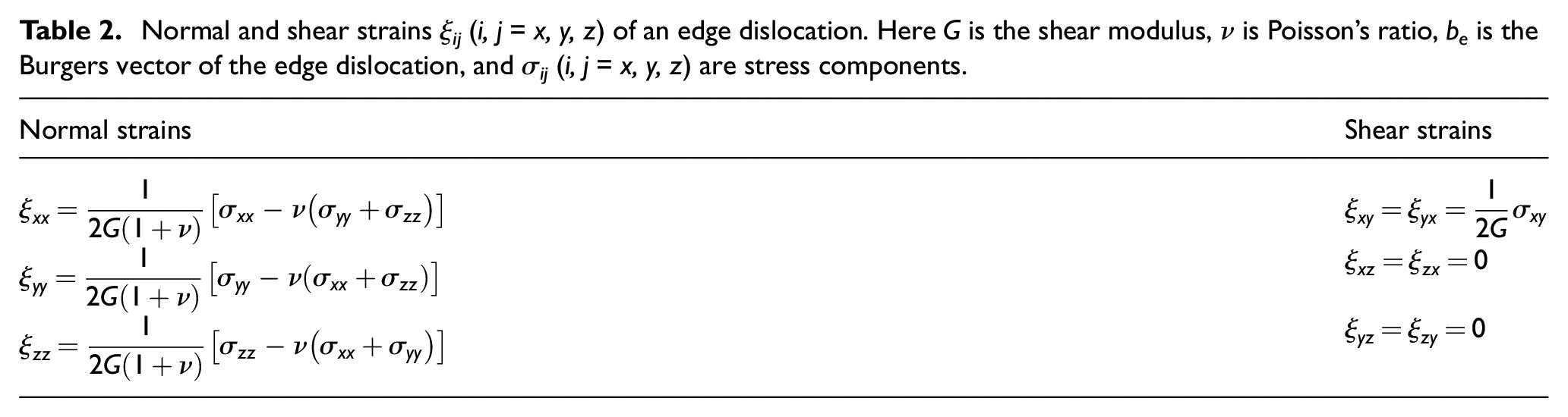
The stress field generated by a straight edge dislocation [45] is given in Table 1 and the corresponding strain field [45] is given in Table 2. Thus, based on equation (2), the induced electric field surrounding an edge dislocation is given by
Normal and shear stress components σij (i, j = x, y, z) of an edge dislocation. Here G is the shear modulus, ν is Poisson’s ratio, be is the Burgers vector of the edge dislocation, and σij are stress components.

Normal and shear strains ξij (i, j = x, y, z) of an edge dislocation. Here G is the shear modulus, ν is Poisson’s ratio, be is the Burgers vector of the edge dislocation, and σij (i, j = x, y, z) are stress components.
For a cubic lattice such as simple cubic (SC) lattice, body-centered cubic (BCC) lattice, face-centered cubic (FCC) lattice (for example, diamond crystal structure, zinc blende crystal structure) and so on, owing to the crystalline symmetry, the following relations may exist:
and
where V, V0, and ξ denote the unit cell volume, unstrained unit cell volume, and shear strain. Hence, the electric field around an edge dislocation is
Substitute the strain components in Table 2, and we have
According to the stress component σzz in Table 1, we have
Substituting expressions for the stress components in Table 1, one may easily obtain the electric field around an edge dislocation
In terms of simple calculations, the electric field around an individual edge dislocation is
where parameters m and n are
ν is Poisson’s ratio, and
In the case of screw dislocation in a cubic lattice, e.g., SC, BCC, and FCC lattices. The strain field components of a screw dislocation gives [45]
After simple derivations, the electric field around an individual screw dislocation is
For electric fields of an edge dislocation and a screw dislocation, the parameters m, n play a key role and should be discussed in some situations. As for some crystals at uniform temperature, strain differences may sometimes cause redistribution of constituents, e.g., impurity atoms, vacancies and interstitial atoms in crystals, ions in ionic crystals, and so on. Their transport and redistribution can also generate local alterations of FSE, so that FSE may be described by
showing that equation (2) is changed from a partial differential form to be a complete differential form. The electric field of dislocations for an ionic crystal with cubic lattices such as NaCl crystal may also be described by equations (3) and (4) and the correlated results for electric forces in the following parts may also be valid, but the only alterations is that the important parameters m and n should take the complete differential form:
3.2 Electric force between dislocations
As far as is known, dislocation dynamics is mostly concerned with the realm of material plasticity. For plastic deformations of materials, most researchers only consider the mechanical force between dislocations, but neglect another vital force, namely, the intrinsic electric force between dislocations. In the following, we reveal this electric force.
Here the general electric force between any two dislocations is discussed first. The electric force between dislocations is equivalent to the force felt by a dislocation under the electric field produced by another dislocation. Also of note is that the electric field generated by a dislocation is always perpendicular to its dislocation line. Therefore, for a dislocation under a complex electric field, the related electric interaction energy in a plane perpendicular to the dislocation line is
Hence, the total electric force exerted on the whole dislocation line is
Of note is that equation (6) may apply for edge dislocations, screw dislocations, and mixed ones. Owing to the superposition principle of strain fields and stress fields [35], the electric fields generated by dislocations may also obey the superposition principle according to equation (2). Meanwhile, in analogy with the fact the strain energy is proportional to the square of strains, the electric energy is also proportional to the square of electric fields. Therefore, the electric energy and related electric force between a pair of any dislocations may not be influenced by other dislocations, and the superposition principle is available for the electric force of dislocations. In the following discussion, the electric forces between parallel straight dislocations will be taken as an introductory example.
3.2.1 Electric force between edge dislocations
Based on equation (3), the electric field around an individual edge dislocation could be written as
For most cubic materials, the normal strains could change the unit cell volume, thereby altering electron density, which may further induce lift of FSE. However, shear strains cannot cause variation of the electron density so that they may lead to much smaller lift of FSE than normal strains. Hence, the relation between parameters may fulfill m>>n. Based on equation (5), the electric interaction energy between two parallel straight edge dislocations is
where r is the distance between the two dislocations, L is the dislocation length, and be1 and be2 are Burgers vectors of the two edge dislocations. Thus, the related electric force per unit length is
where

The ratio between electric force Fe and Peach-Koehler force FPK depends on distance and product εm2 (ε denotes dielectric constant and m is parameter). For a crystal with shear modulus G = 50 GPa, and Poisson ratio ν=0.3, the red line displays the region (cyan colored) where the magnitude ratio Fe/FPK>1, and the black line shows region (cyan and yellow colored) where the magnitude ratio Fe/FPK>0.1.
3.2.2 Electric force between screw dislocations
Like the foregoing treatment, the electric force between two parallel screw dislocations may be derived in terms of electric interaction energy. Based on equations (4) and (5), the electric interaction energy may be given by
where bs1 and bs2 are Burgers vectors of the two screw dislocations, L is the length of screw dislocations, and r is the distance between two dislocations. Thus, the electric force between two parallel screw dislocations of unit length at a distance r is
Analogous to the situation of edge dislocations, electric force between screw dislocations decreases rapidly with distance and may be ignored at large distances. However, if the distance is only several nanometers and the dielectric constant is large, the electric force may be evident, which can affect plastic deformations of materials.
3.2.3 Electric force between screw and edge dislocations
In terms of electric fields of edge and screw dislocations, the electric interaction energy between an edge dislocation and a parallel screw dislocation (the dislocation line is parallel to each other) is obtained based on equation (5)
where be and bs are the magnitude of the Burgers vector for the edge dislocation and screw dislocation, respectively. Here be is always positive; bs is positive if it is parallel to its dislocation line, but negative if it is antiparallel to dislocation line. Again L is the dislocation length and r is the distance between the two dislocation lines. Thus, the electric force between the two parallel dislocations of unit length at a distance r is
This equation indicates that the electric force depends on the dielectric constant and is also inversely proportional to the cube of distance. As demonstrated, an intrinsic electric force always exists between an edge dislocation and a parallel screw dislocation. Considering the fact that forces between an edge dislocation and a parallel screw dislocation has never been considered owing to the absence of the Peach–Koehler force [49], this electric force may be important.
3.2.4 Correction for image force
The image force of a dislocation near a planar grain boundary may be regarded as the interaction between a dislocation and its image dislocation. The classical image force of dislocations only considers the mechanical force and neglects electric force [45, 47]. Based on the previous discussions, the image forces should be corrected according to the electric force between dislocations, and the related corrections for an edge dislocation and a screw dislocation are
where d is the distance from the planar grain boundary, be and bs are Burgers vectors of the edge dislocation and image dislocation, as shown in Figure 2, and Fe and Fs are the corrected image forces for an edge dislocation and a screw dislocation, respectively. In Equations (13) and (14), the first term is the mechanic force [45, 47] and the second term is the electric force. The electric forces are also attractive and are in the same direction as the mechanical forces. As pointed out previously, for metals and materials with high dielectric constant, the corrected electric forces may be of paramount importance.

Dislocations near the planar grain boundary and their image dislocations: (a) an edge dislocation (in red) and its image dislocation (in dashed red) at a distance d away from the grain boundary and their Burgers vectors at the x axis; (b) a screw dislocation (in red) and its image dislocation (in dashed red) at a distance d from grain boundary, and their Burgers vectors are directed perpendicularly out of the screen and into the screen, respectively.
For electric forces between dislocations, several points need to be emphasized here. First, electric forces between dislocations were discussed in piezoelectric materials [49], but the existence of electric forces between dislocations revealed in this work may be intrinsic, ubiquitous, and applicable for all crystals with any symmetry, not just restricted to piezoelectric materials. Second, for metals, the electric force may be so noticeable that it may dominate dislocation dynamics. Third, conclusions upon plastic deformations, as are built on classical dislocation dynamics where the electric force has been neglected [48], e.g., DDD [31–42], may need to be re-examined carefully by adding the electric force. A comparison between this theory and associated experimental observations needs to be performed in the future.
3.3. Dislocation motion under an external electric field
3.3.1 Edge dislocation motion under an external electric field
This electric field around an edge dislocation would influence electrical conductivity of crystals and can give rise to the electric energy of a dislocation, as discussed previously [43]. If an external electric field
where ε0 is the vacuum dielectric permittivity, ε is the relative dielectric constant, L is the dislocation length, and φ is the polar angle of dislocation. As pointed out previously, the magnitude of parameter m may be much larger than n for many materials. Thus, if the external field is parallel to the Burgers vector, i.e., ψ=0, the electric energy is
It is easily seen that when m>0, this energy is the smallest at polar angles 3π/4 and 7π/4, meaning that dislocations (1) (in red color) may remain in the most stable state in the external electric field, as shown in Figure 3(a). However, at polar angles π/4 and 5π/4, W12 is the highest, indicating that dislocations (2) (in blue color) may undergo an electric force pointing to dislocations (1) shown in Figure 3(a). The electric force component F in the gliding plane for a unit length dislocation may be

Edge dislocations in a crystalline grain under an external electric field
where r0 is the distance of the dislocation away from the center axis of the crystalline grain. Under some conditions, e.g., high temperatures and large external electric field, the electric force may exceed the Peierls–Nabarro stress [45] and enables edge dislocations to glide. Thus, a threshold electric field Eth exists above which the edge dislocations can be driven to overcome motion barriers and glide,
where G is the shear modulus and a is a crystalline lattice parameter. This threshold field is highly dependent on the distance r0, dielectric constant ε, and polar angle of this edge dislocation. The existence of the threshold electric field was evidenced by experimental data in alkali halide crystals [7, 15, 16]. Based on analytical expressions of the flexoelectric coefficient [43], the parameter m can be written as
respectively.
If the Burgers vector is perpendicular to the electric field, i.e., ψ=π/2, the electric interaction energy is
In addition, a corresponding threshold electric field Eth exists and it is
For many crystalline materials, the threshold fields at different conditions may be in the range 104–106 V/m, and it may decrease with increasing temperature because of material softening and increased relative dielectric constant. These points were verified by electric field-driving motion of small angle–tilt grain boundaries constructed by array of edge dislocations [7]. Furthermore, according to the expressions of electric forces in the above two cases, the forces are positive in some polar angle zones but negative in other angle zones. Therefore, under an electric field, some dislocations are expected to glide in a direction, but some other dislocations are anticipated to move in the reverse direction, which is indeed the experimental observations that the majority of dislocations move against the field, but a large proportion still move in the field direction in sodium chloride [1, 50, 51]. For some metals, owing to their ultra-large static dielectric constant, a small pulsed electric field may enable some dislocations to glide and a stronger electric field can drive more dislocations to glide, which may result in a noticeable reduction of flow stress in the plastic deformations. This is the observed for electroplasticity of metals [19] and may be the underlying physical origin. Despite the theory being in qualitative agreement with related experiments, a more detailed comparison between this theory and experiments is still needed in the future.
Edge dislocations can be driven to move by an electric field, but against previous numerous investigations on the debated charges of edge dislocation [9, 10, 20, 21, 47], here it is found that dislocations themselves do not actually carry net charges, so that mobile edge dislocations do not contribute to electrical conductivity, but they can affect electron mobility, thereby influencing the electrical conductivity of materials.
3.3.2 Screw dislocation motion under an external electric field
Based on equations (4) and (5), owing to rotation symmetry of a screw dislocation, the electric interaction energy between a screw dislocation and an external electric field
where ψ is angle between the electric field and transverse axis where a screw dislocation is situated. In the case of positive parameter n, this energy is the smallest at angle π/4, meaning that dislocations (1) (in red color) remain in the most stable state in the external electric field, as shown in Figure 4. However, at angle 5π/4, W12 is the largest, indicating dislocations (2) (in blue color) may undergo an electric force. The magnitude of electric force for a unit length dislocation may be

Screw dislocations in a crystalline grain in an external electric field and the Burgers vector upwards through the paper. If the parameter
and its direction is tangentially pointing to dislocations (1) shown by the arrows in Figure 4. This force sensitively relies on the angle and distance from grain center axis, and may drive some dislocations into zones of dislocations (1), thereby forming dense zones and sparse zones of screw dislocations. If the sign of parameter n or the Burgers vector possesses a negative value, the electric interaction energy and the electric force may also be reversed.
Interestingly, like edge dislocations, screw dislocations can be driven to move by an external electric field, but they do not carry net charges by themselves.
In the analysis given here, only the strain field of a dislocation is considered, and its image dislocation and grain boundary relaxation effect on the strains and electric field in the grain have been ignored.
4. Conclusions
In summary, we have mainly explored electric features of dislocations and revealed an electric field around a dislocation, which leads to an important intrinsic ubiquitous electric force between dislocations. The electric force was uncovered here first, and it was found to be important and could surpass the classically known Peach–Koehler force for metals and materials possessing ultra-large dielectric constant. Thus, the electric force may be important for dislocation dynamics and related material plasticity. On the other hand, dislocations were found to be subject to an electric force under an external electric field. A threshold electric field was discovered, above which the electric force for dislocations under the external electric field enables dislocations to glide. Owing to the electric field-induced electric force, some dislocations move in one direction, but others move in reverse, which may explain the experimental results that have puzzled people for a long time. The electric properties of dislocations and the intrinsic electric forces between dislocations is anticipated to help people re-understand dislocation dynamics and related plastic deformations of materials.
