
Abstract
The use of 3D printers and plating is an effective method for prototyping expensive high-frequency components easily and at low cost. The purpose of this study is to monolithic mold a millimeter-wave waveguide bandpass filter (BPF) with a fine structure. We propose a new structure which is suitable for the 3D printing, and introduce the FDTD method (finite difference time domain method) and µGA (micro genetic algorithm) in its design. It is confirmed from the prototype and measurement results that the filter properties are obtained with the proposed structure.
Introduction
The use of 3D printers and plating to manufacture high-frequency components such as waveguides is attracting attention.1,2 This method has the advantage of being inexpensive to manufacture and highly customizable. To confirm the reproducibility of 3D printers in millimeter-wave band, we focus on waveguide filters with fine structures. Millimeter-wave waveguide bandpass filters (BPFs) are essential components for millimeter-wave communications and low-loss communications in aerospace applications. 3 However, the high-precision 3D printers used to prototype millimeter wave band components are extremely expensive.
The purpose of this study is to prototype millimeter-wave waveguide bandpass filters with fine structures using general-purpose 3D printers and plating. Prototyping using a general-purpose 3D printer can significantly reduce prototyping costs compared to using a high-precision 3D printer. Since BPFs with conventional structures are difficult to prototype with 3D printers, we propose a new BPF structure which is suitable for 3D printers. To design the proposed structure, a metaheuristic design method that combines the FDTD method (finite difference time domain method) and µGA (micro genetic algorithm) 4 is introduced. Finally, it is demonstrated that the general-purpose 3D printed waveguide has sufficient transmission characteristics.
Analysis model and design method
Analysis model
Figure 1 shows the analysis region of a waveguide BPF. The cell size of the FDTD method is 0.1 mm. WR-19 (4.8 × 2.4 mm) standard waveguide is modeled, and three windows are placed in the center. Non-reflection terminations are inserted at both ends of the waveguide. The window consists of an inductive iris and a capacitive post, and the transmission frequency band is determined by changing the iris width w and the post height h. The window structure shown in Figure 2(a) is conventional, but this structure which includes sudden rises and falls is difficult to prototype with a 3D printer. Therefore, in this study, we propose to use the structure shown in Figure 2(b) considering the printing angle of the 3D printer. Because the proposed window structure is completely inapplicable to conventional design methods, 3 a highly versatile design method is required, which is discussed in the next section.
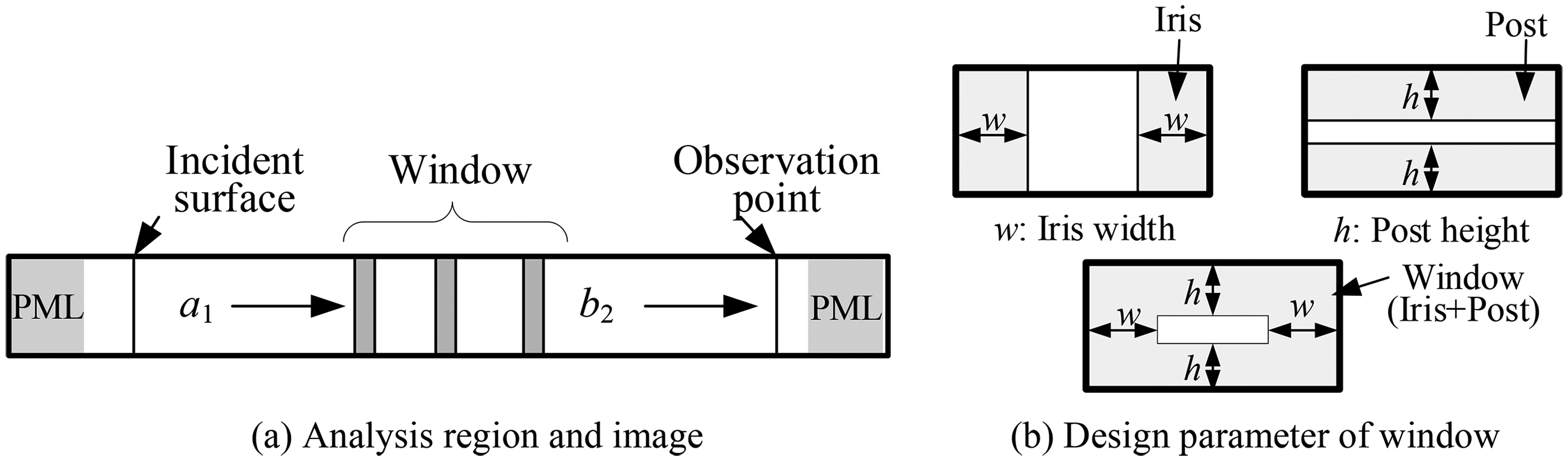
Analysis model. (a) Analysis region and image. (b) Design parameter of window.
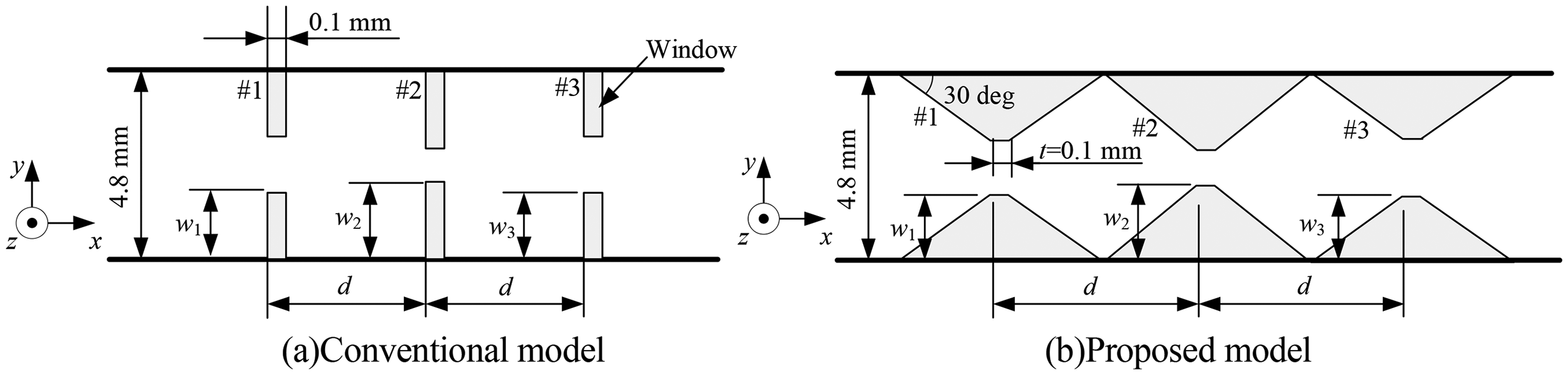
The cross-section of waveguide BPF (top view). (a) Conventional model. (b) Proposed model.
Design method
We attempt to design BPF with a transmission frequency of 50 GHz within the range of the waveguide usage band of 40–60 GHz. The wavelength in this frequency band is 5.0 to 7.5 mm. In this study, the design parameters are the iris width w, the post height h, and the window distance d, and these design parameters are designed by μGA. The range of the iris width w is set to 0.9 to 2.2 mm, the range of the post height h is set to 0.0 to 1.0 mm, and the window position d is set to −0.3 to +0.3 mm based on 1/2 or 3/4 of the waveguide wavelength. The window #1 and #3 in Figure 2 have the same size to realize bidirectionality. Since μGA performs optimization using a relatively small number of individuals, it is a method suitable for optimization design using the FDTD method which requires computational time. In this study, the number of individuals is set to five. After generating the initial individuals, µGA repeats the following steps.
4
Evaluation of each individual using the FDTD method Ranking Elite saving Individual generation by crossover processing
If individuals become similar, there is a possibility of falling into a local solution. Therefore, the convergence check is performed for each individual. When all the parameters of each individual are the same, it is judged that all individuals have converged. If the convergence occurs, individuals other than the elite individual are randomly generated.
The objective function OF used for evaluation is as shown in equation (1).

The first term is the transmission coefficient s21 of the scattering parameter of the peak frequency within the usage band, and s21 is calculated as s21 = b2/a1 in Figure 1. The second term bw indicates the bandwidth of the peak frequency, and the third term Δf indicates the difference of the peak frequency from the design frequency (50 GHz). All terms are normalized because they have different dimensions, and the second and third terms are adjusted by weighting coefficients W1 and W2. In this optimization, the optimization converged within 200 generations. The calculation time up to 200 generations was about 38 min using the Hokkaido University supercomputer system (FUJITSU Server Primergy CX400/CX2550 M4).
Optimization results
The filter characteristics shown in Figure 3 are obtained when d = 3.8 mm in the conventional structure and 5.6 mm in the proposed structure. At frequencies higher than the transmission frequency, the frequency characteristics tended to be similar, but at lower frequencies, the spectra of the proposed structure are larger than that of the conventional structure. Figure 4 shows the design results for both. The proposed structure consists of only Iris. Figure 5 shows the frequency characteristics of the proposed structure when w of each iris is changed. As the width w decreases, the transmission frequency tends to shift to the lower frequency side. The above results show that the transmission frequency can be controlled by adjusting the width of the iris.
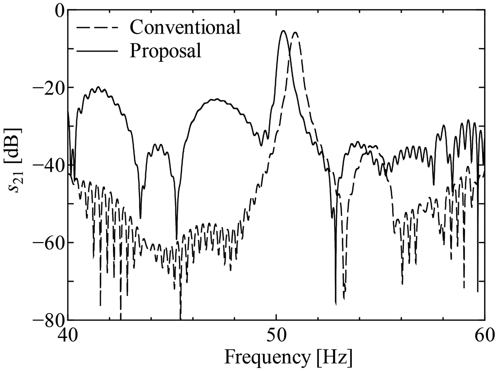
Transmittance characteristics of optimization results.
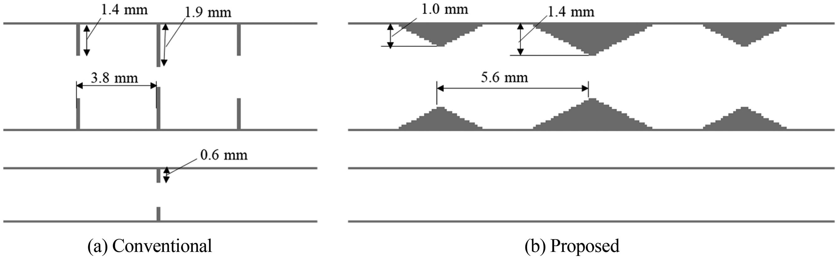
Cross-section of optimization results (upper: top view, lower: side view). (a) Conventional. (b) Proposed.
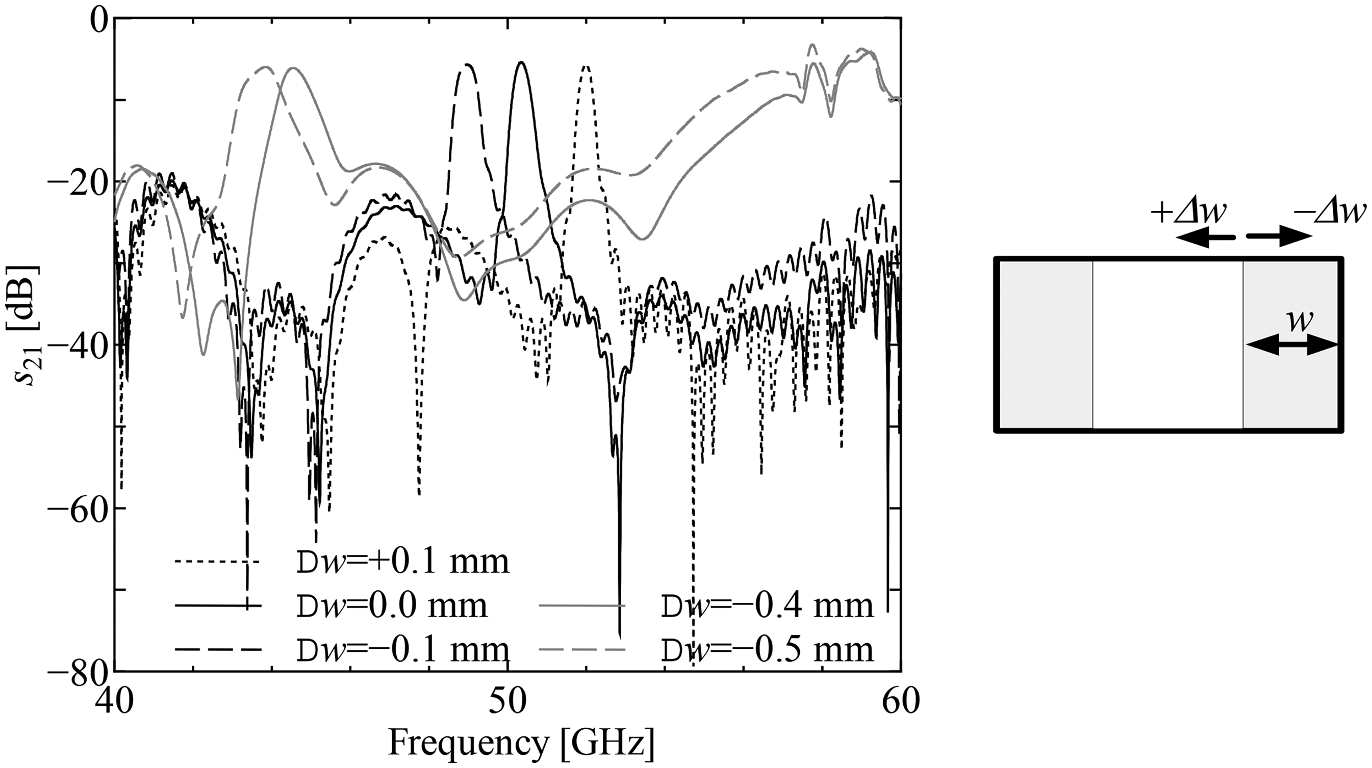
Calculation results of the proposed structure when Δw is changed.
Prototype and measurement
Prototype of BPF
The 3D printer used in this study is a fuzed deposition type MAESTRO 2.5 EX. The printing pitch is 0.01 mm, the nozzle diameter is 0.4 mm, and it can print at offset angles of up to 60 degrees even without support material. Conductive PLA (polylactic acid) was used as the filament material. The outer dimensions of the prototype are 30 × 30 mm considering the flange dimensions of the coaxial waveguide converter.
Next, the 3D printed products were nickel plated. In this study, electroless nickel plating was used, so plating can be performed with laboratory-level equipment such as a beaker for dipping the nickel plating solution, and a temperature-adjustable heater. Although the nickel plating is insufficient for use as a product, this is not a major problem for small-lot prototype. The nickel plating was performed in the following steps.
(a) Washing (b) Drying (c) Put in palladium chloride aqueous solution and reduce (d) Plating in nickel plating solution
The plating thickness changes depending on the plating time. In order to determine the appropriate plating time, we produced prototypes with three different plating times: 60, 90, and 120 min.
Measurement
The photograph of the prototype is shown in Figure 6(a). The prototype is made with a length of 20 mm. The hole is drilled in the aperture of the waveguide to attach the coaxial waveguide converter. The cross-section of the prototype is shown in Figure 6(b). The designed structure is almost exactly reproduced, and it is confirmed that the inside of the waveguide is plated. The transmittance coefficient s21 was measured in the 40 to 60 GHz band by using the vector network analyzer (Rohde & Schwarz ZVA67).
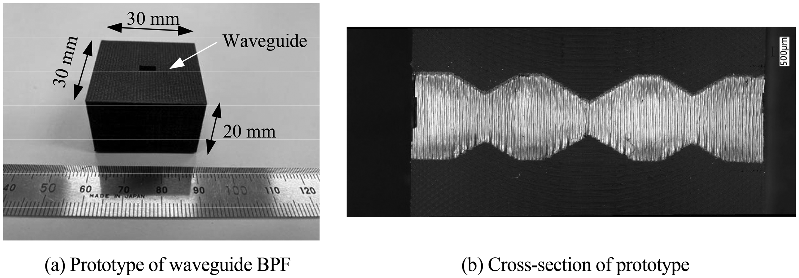
Photograph of prototype. (a) Prototype of waveguide BPF. (b) Cross-section of prototype.
First, the straight waveguides are prototyped and measured to evaluate plating performance. As shown in Figure 7, Although attenuation of approximately 0.3 to 0.4 dB are observed compared to the characteristics of a coaxial waveguide converter alone, flat frequency characteristics within −1 dB are obtained in the measurement frequency range. By comparing the plating times, the plating time for the waveguide BPF is determined to be 60 min.
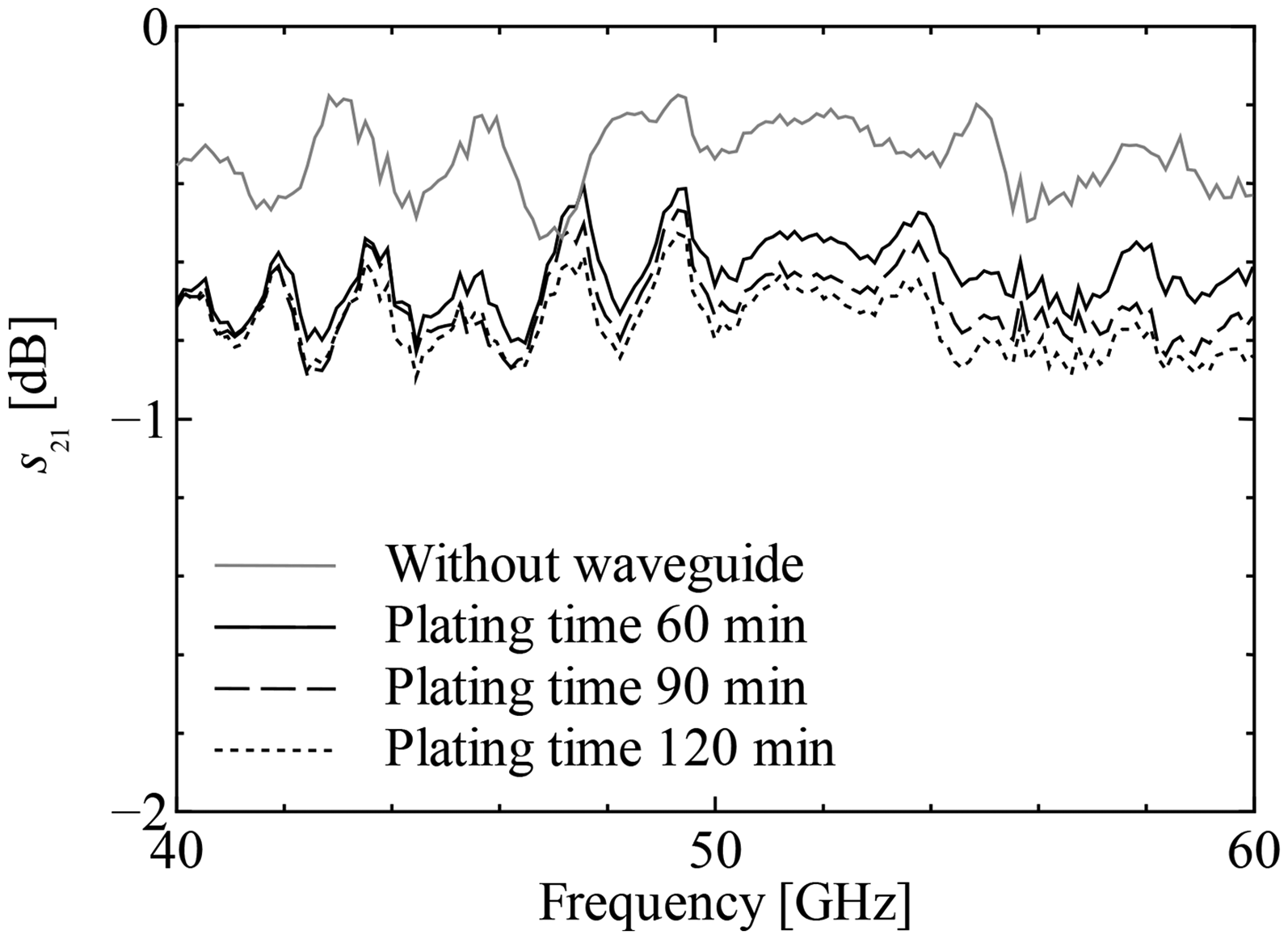
Measurement results of waveguide.
Next, Figure 8 shows the measurement results of the waveguide BPF. Although the peak frequency is appeared at approximately 43 GHz, which is lower than the design value, it is confirmed that the prototype functions as a bandpass filter. Since the optimization results are almost reproducible from Figure 6(b), the future work is to clarify the cause of the shift in transmission frequency. Furthermore, it is confirmed that the transmission frequency can be changed by changing the iris width w. This trend is similar to the calculated results. On the other hand, there was a tendency for the attenuation to increase as the transmission frequency is shifted toward higher frequencies.
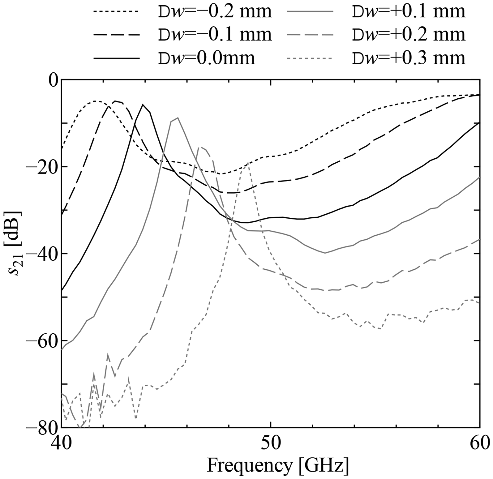
Measurement results of BPF.
Conclusion
In this study, we have demonstrated that it is possible to prototype the waveguide and the waveguide BPF in the 40 to 60 GHz band using general-purpose 3D printer and plating. Millimeter-wave components are generally prototyped in parts, the 3D printer can make the waveguide BPF in one piece. Another advantage of this prototype method is that 3D printed products are lighter than the conventional metal one.
In the future, we plan to correct the frequency difference between the design results and the measurement results, and develop new window structure that can control the bandwidth. we plan to perform multi-objective optimization that not only maximizes the transmission coefficient but also achieves broadband at the same time.
Footnotes
Acknowledgements
This work was supported by the Telecommunications Advancement Foundation and the Cooperative Research Project of the Research Institute of Electrical Communication, Tohoku University. In addition, this work was partly supported by the collaborative research program, information initiative center, Hokkaido University.
Funding
The author(s) received no financial support for the research, authorship, and/or publication of this article.
Declaration of conflicting interests
The author(s) declared no potential conflicts of interest with respect to the research, authorship, and/or publication of this article.