
Abstract
Piezoelectric Micromachined Ultrasonic Transducers (PMUTs) have shown great potential in biomedical applications, yet conventional micro-scale PMUTs face challenges due to thick diaphragms and large membrane dimensions, which limit electromechanical coupling and reduce acoustic output. Also, full-area electrodes often excite unwanted higher-order vibration modes, while small electrodes limit the effective coupling. Thus, this research offers a solution to these problems by proposing a Nano-Scale Circular Double-Lamination AlN-based PMUT design. The proposed design reduces the diaphragm radius to 500 nm, improving strain transfer and electromechanical coupling. Additionally, this design adopts a partial electrode configuration of 156.25 nm with a top central electrode to enhance the electric field, while eliminating higher-order vibration modes and maximizing displacement at the diaphragm. Moreover, PZT's complex perovskite crystal structure and polarization mechanisms cause a high dielectric constant and dielectric losses, which restrict its use in implantable devices. Thus, this design uses lead-free Aluminum Nitride (AlN) with a wurtzite crystal structure, which provides low dielectric loss and ensures efficient energy conversion even at high frequencies. COMSOL Multiphysics simulations demonstrate a resonant frequency of 18.883 MHz, a broad bandwidth of 10 MHz, an energy density of 1.8 J/m3, and high central displacement, making the device ideal for high-frequency superficial clinical imaging and wearable biomedical applications.
Keywords
Introduction
In biomedical applications, finger vein patterns provide a more secure method of authentication in which ultrasonic sensors and transducers hold great promise. Traditional transducer designs exhibit low impedance, while MEMS ultrasonic transducers (MUTs) have a relatively high acoustic impedance match. Acrylic MEMS ultrasonic transducer (CMUTs) and Piezoelectric Micromachined Ultrasonic Transducers (PMUTs) are both constructed based on their respective actuation mechanisms.1,2,3,4 CMUTs need a narrow gap height in order to function efficiently, while PMUTs are based on the piezoelectric effect, and are not constrained in deflection by a narrow gap height. Piezoelectric effect is one of the processes that produce ultrasound, which is utilized to operate PMUTs, to experience tension or strain.5,6,7,8 PMUTs employ a variety of piezoelectric materials, which determines its electromechanical performance and resonance frequency. Polyvinylidene fluoride (PVDF) is not suitable for MEMS technologies, lead zirconate titanate (PZT) thin films are the most extensively investigated ferroelectric materials. There are many methods to deposit thin PZT films methods such as sputtering, sol-gel, and metal organic chemical vapor deposition9,10,11 Aluminum Nitride (AlN) and Zinc Oxide (ZnO) are common piezoelectric materials that use non-ferroelectric deposition. ZnO have issues with high dielectric loss at low frequency and rapid Zinc ion diffusion and sol-gel, chemical deposition and sputtering techniques require high temperatures. PZT have challenges with thin film deposition due to temperatures that MEMS restricts from CMOS.12,13,14,15 Another challenge is that any deposition done at high temperature has a chance of ejecting toxic lead in the air. Therefore, there is a need for ultra-miniaturized, high-performance PMUT suitable for wearable and implantable biomedical applications.
Main contribution
Thus, this work proposes a circular double-lamination PMUT with nanoscale diaphragm dimensions, which optimizes electromechanical coupling and reduces acoustic impedance mismatch. To maximize electromechanical coupling and acoustic output, a partial electrode configuration is used, with a central top electrode and an annular bottom electrode, which concentrates strain at the diaphragm center while suppressing higher-order vibration modes. This design utilizes AlN as the active piezoelectric layer, achieving low dielectric loss, high-frequency stability, and biocompatibility.
Therefore, this work is divided into the following sections, the first of which is the introduction. Section 2 discusses the existing literature on various PMUT designs. Section 3 explains the proposed PMUT design and its workflow. Section 4 describes the experimental investigations and the performance and comparative analysis of the proposed design. The paper is finally concluded in the final Section 5.
Literature survey
Wang et al. 16 created a 2 × 2 piezoelectric scalar hydrophone array and an MCU-based signal-conditioning circuit to create an acoustic pressure-gradient MEMS vector hydrophone system. The proposed system uses a directionality identification algorithm to recognize the received signals and give the azimuth angle of the underwater acoustical pressure signals. Sputtered potassium sodium niobate films were utilized by Xia et al. 17 to illustrate air-coupled pMUTs with high SPL at low driving voltages According to pulse-echo-rangefinder measurements, the single pMUT gave a good transceiving ability. Using AlScN PMUTs as the basis, Li et al. 18 concentrated on creating a miniature Ultrasonic wireless power transfer technology receiver device. The rectified energy produced by the device was successfully used to power commercial LED devices. Zhang et al. 19 developed a variety of PMUT devices with various top electrode shapes, such as square, circular, and doughnut. The findings demonstrate that the circular electrode PMUT was better suited for creating high-density arrays. The micro-hole inter-etch and sealing method was used by Wang et al. 20 to build the cavity diaphragm structures for PMUTs. By using a sputtering approach, AlN PMUT arrays of various sizes and shapes were effectively produced. Liu et al. 21 built and analyzed a PMUT device using polarized, lead-free, highly efficient Na0.5Bi0.5TiO3-BaTiO3 (NBBT) piezo single-crystal films. It demonstrated the potential of the PMUT device, on lead-free piezoelectric single-crystal NBBT films in extreme-frequency and superior-resolution medical ultrasound imaging. Wu et al. 22 developed an AlN-derived PMUT panel for non-invasive radial artery stiffness monitoring, which is utilized in applications for vascular health monitoring in humans. The radial artery's constant dynamic alterations were documented using the PMUT device as an ultrasound probe. Chen et al. 23 looked into the electromechanical-acoustic multi-field coupling mechanism and the array technology for the design of MEMS advanced PMUT ultrasonic transducer components. Using a transferred periodically poled piezoelectric film (P3F) Xcut lithium niobate (LN), Yao et al. 24 produced a prototype bi-layer PMUT. It established bi-layer P3F LN PMUTs as a promising platform for compact, high-performance ultrasonic transducers. Liechti et al. 25 presented the modeling and characterization of AlN-based PMUTs for biological applications. Empirical corrections were utilized from large-scale finite element method to provide more accurate results.
such as limitations in miniaturization, reduced performance in real-world application, unsuitable for ultra-small devices, issues in different ambient conditions, complications in precise diaphragm control, limited penetration depth, limitations in durability and large scale validation, low sensitivity and scalability in large unit size, need of improvement in coupling and integration and trade-offs between electrode design, pressure output, and bandwidth.
Current state-of-the-art
The nano-scale PMUTs are used widely around the world because of their reliability in various fields such as bio-medical imaging, sensing and therapeutic applications. The traditional methods used lot of materials for the production of PMUTs such as AlN, lead, ZnO and etc. The lead induced piezoelectric material is majorly used in the production of the PMUT devices. In traditional the thickness of the diaphragm used in the production is usually large and the size of the framework is also big; they did not have any miniature design of PMUT. Furthermore, the existing techniques had considerable amount of challenges in real-world application as the models possess issues in different ambient conditions.
The full area electrodes are used in conventional methods in electrode configuration for the process of electrochemical coupling. The traditional methods mostly consist of structures such as, complex perovskite crystal structure and polarization mechanisms in their framework or design. Lead is one of the major components in the structure of the existing techniques, which always dissipated into the environment, because of the heat. The existing techniques also needed improvement in pressure output and bandwidth.
Although significant progress has been made, several limitations remain across recent PMUT studies. Thus, a novel nanoscale PMUT design is needed to achieve higher sensitivity and better electromechanical coupling while enabling dense integration for miniaturized biomedical devices. It also addresses limitations of bulky structures by enhancing performance in air/liquid coupling and suitability for implantable applications.
Motivation for this work
In conventional micro-scale PMUTs, one major drawback is suboptimal electromechanical coupling efficiency, which arises from the combined effects of a relatively thick diaphragm stack and large diaphragm dimensions. In the case of these devices, the diaphragm is often several times thicker than the piezo layer, causing mechanical stiffness to be dominated by the diaphragm. Thus, the thin piezoelectric film does not completely deform or transfer strain efficiently. These factors reduce the efficiency of converting electrical energy into mechanical vibration, leading to a narrower bandwidth and diminished acoustic output. The conventional designs of bulk and micrometre-scale PMUTs lack the structural miniaturization needed for efficient integration into wearable or implantable platforms, thus limiting their versatility to modern biomedical needs.
Additionally, many conventional designs face challenges in electrode configuration. Designs that use full-area electrodes often excite unwanted higher-order vibration modes, reducing sensitivity, while designs with overly small electrodes limit the effective electromechanical coupling. This mismatch in electrode coverage reduces the piezoelectric activity at the center of the membrane, where the displacement is greatest, further downgrading the overall performance. A clear design framework for optimized partial electrode geometries, which maximizes displacement at the diaphragm center while suppressing higher-order modes, is still lacking.
Conventional PMUTs with PZT thin-film layers are thus considered high in electromechanical coupling and powerful in acoustics. However, long-term reliability and efficiency are impeded by material constraints. Specifically, due to the nature of fundamental material properties such as its complex perovskite crystal structure and polarization mechanisms, PZT experiences a high dielectric constant and high dielectric losses, 26 which means energy is dissipated at high oscillating-wave frequencies, thereby limiting high-frequency operation and low sensitivity for nanoscale devices. Additionally, the presence of lead in PZT raises serious environmental and biocompatibility concerns, making it unsuitable for biomedical and implantable applications.
These drawbacks encouraged the search for better lead-free piezoelectric materials with high stability, and emphasize the necessity of PMUT designs that strikes a good balance of diaphragm stiffness, piezoelectric layer thickness, and electrode placement for the best electromechanical coupling, as well as superior biocompatibility for the biomedical PMUTs of the next generation.
Proposed PMUT design
Thus, to address these issues, this work introduced a Nano-Scale Circular Double-Lamination AlN-Based Piezoelectric Micromachined Ultrasonic Transducer (PMUT) Design. Here, the diaphragm size is scaled to the nanometer, and by optimizing the lamination structure, it helps to make the electromechanical coupling better, reduce impedance mismatch of acoustics between all layers. In addition, putting forth a lead-free AlN reduces environmental toxicity and is biocompatible, an important factor in wearable and implantable biomedical applications. This architecture also allows greater flexibility in frequency tuning through diaphragm geometry and lamination ratios rather than piezoelectric thickness alone.
Material selection
In Piezoelectric Micromachined Ultrasonic Transducers
Piezoelectric layer
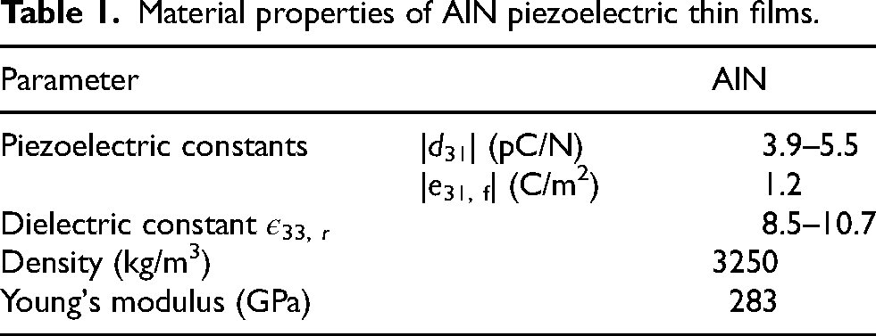
In this work, AlN was selected as the active piezoelectric thin film. The complex perovskite structure and polarization mechanisms of PZT cause losses in existing designs, despite its high electromechanical coupling. This results in energy dissipation at high frequencies and decreased sensitivity in nanoscale diaphragms. On the other hand, AlN's inherent low dielectric losses due to its simpler wurtzite crystal structure allow for effective energy conversion even in extremely thin diaphragms, which is essential for high-frequency operation. AlN's moderate dielectric constant maximizes electromechanical coupling and improves polarization efficiency without causing a large amount of energy dissipation by concentrating the applied electric field within the active layer. Moreover, AlN is lead-free and CMOS-compatible, facilitating monolithic integration with electronic circuits, directly overcoming the environmental and health concerns posed by PZT, making it suitable for implantable and wearable biomedical devices. The material constants for AlN thin films as summarized in Table 1.
Material properties of AlN piezoelectric thin films.
Effective bidirectional transduction is made possible by the c-axis polarization along the film thickness, which means that the diaphragm senses incoming acoustic signals using the direct effect and produces ultrasonic waves using the inverse piezoelectric effect. AlN is a strong material for both transmission and reception in nanoscale ultrasonic sensing because of its dual response. This combination of mechanical robustness, biocompatibility, low dielectric loss, and high-frequency stability allows the proposed PMUT design to achieve improved sensitivity, a wider bandwidth, and long-term operational reliability. This effectively addresses the fundamental material limitations of PZT and makes it a good fit for next-generation nanoscale biomedical ultrasonic transducers.
The anisotropic dielectric, elastic, and piezoelectric properties of AlN were specifically specified in the simulation environment to ensure precise Multiphysics modeling of the suggested PMUT. In contrast to isotropic approximations, these tensor-based material parameters accurately predict device performance by capturing the direction-dependent electromechanical response of AlN. The following matrices were utilized in the COMSOL simulation. The Piezoelectric coupling matrix is defined in Equation (1)
27
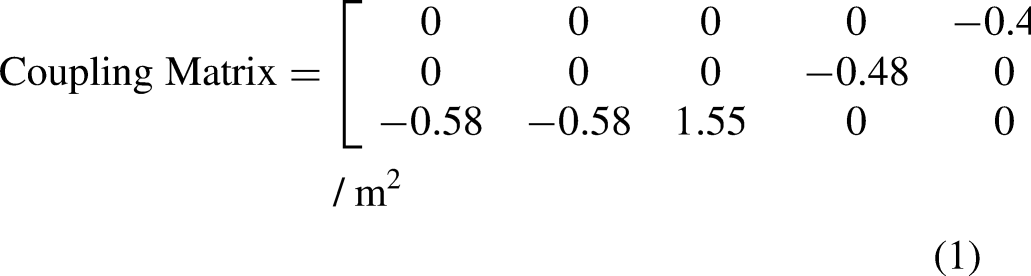
This piezoelectric matrix defines the coupling between mechanical stress and electric field in AlN. It includes both the standard coupling components and the transverse shear components. The dominant term e33 = 1.55 C/m2 corresponds to c-axis polarization, which governs the out-of-plane electromechanical coupling in wurtzite AlN. The relative permittivity matrix is given in Equation (2)
28
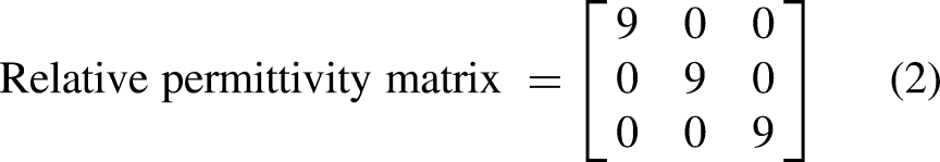
The diagonal nature indicates isotropy in the in-plane directions, while the moderate dielectric constant ensures low dielectric loss at high frequencies. The elastic matrix (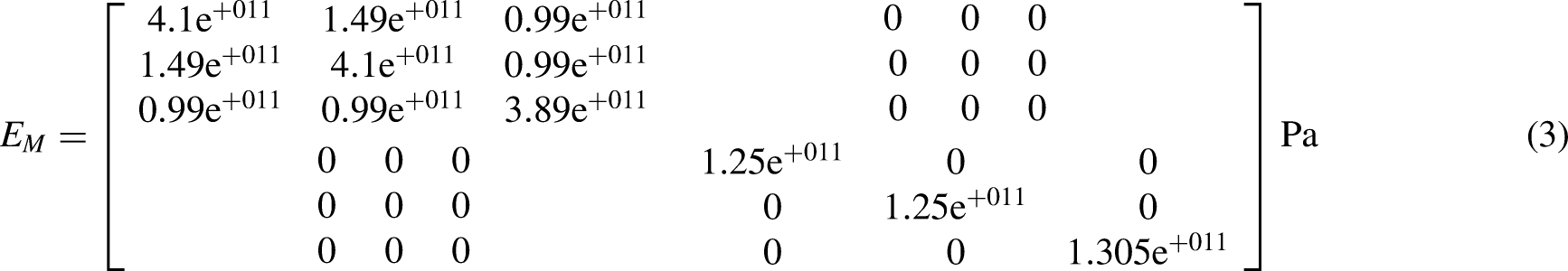
The stiffness matrix is used in COMSOL to represent the stress–strain relations under anisotropic conditions. The values are very close to the elasticity matrix, validating consistency. The stiffness matrix (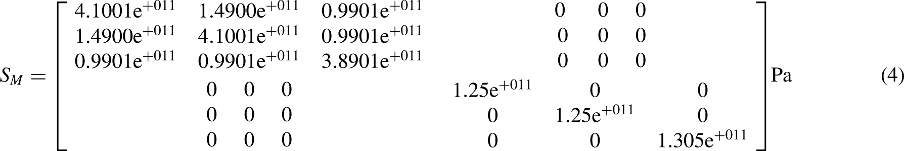
These material parameters accurately represent the anisotropic mechanical and dielectric properties of AlN, which are essential for achieving realistic and predictive simulation outcomes. These parameters enable a realistic simulation of the PMUT's electromechanical behavior under coupled field conditions.
Electrode material (Mo)
Molybdenum is selected as a metal to utilize because it has good electrical conductivity, is mechanically robust, and is amenable to thin film deposition techniques, including sputtering. Unlike Au or Pt electrodes, Mo has a much higher resistance to cracking and delaminating when subjected to repeated cyclic actuation, which is important in ultra-thin, nano-scale diaphragms. Electric potential at an electrode thickness of 20 nm reduces the effective mass loading while retaining good electrical conductance and diaphragm vibration modes. Here utilizes partial electrode coverage, which allows us to enhance the displacement of the diaphragm center while damping higher modes of vibration, avoiding the difficulties of electrode sensitivity experienced with traditional PMUT configurations.
Insulation layer (SiO2)
The SiO2 insulating layer is essential to the proposed PMUT design, as it prevents charge leakage between the electrodes and the piezoelectric layer, ensuring that the structure remains electrically intact during use. The low dielectric constant permits the applied electric field to remain contained in the AlN piezoelectric layer, which improves the polarization and maximizes electromechanical coupling. The SiO2 layer also helps stabilize and reliably diaphragm actuation by decreasing parasitic capacitance and unintended charge redistribution.
Substrate (Si) layer
The Silicon (Si) substrate provides the necessary mechanical support for the multilayer diaphragm. However, the highly thick diaphragm is stiffer and it makes the bending of the AlN sheet harder, which reduces the ability of the model in converting mechanical energy into electrical energy. So, to enable efficient energy transfer, the central region of the substrate beneath each diaphragm is selectively etched to locally reduce its thickness. 29 This substrate thinning lowers mechanical stiffness in the active area, allowing greater out-of-plane deflection of the piezoelectric layer under an applied electric field. As a result, acoustic output pressure and sensitivity are significantly improved, while maintaining structural rigidity around the periphery for mechanical stability.
PMUT design
As the core element of the proposed PUMT array, a nano-scale layered circular diaphragm was designed and modeled using COMSOL Multiphysics. In order to overcome the limitations of current micro-scale PMUTs, including suboptimal electromechanical coupling, limited miniaturization, and inefficient electrode coverage, a circular nano-scale double-lamination design was selected in this research. This design is optimized to provide strong electromechanical coupling in both air and liquid environments while maintaining ultra-miniaturized dimensions suitable for wearable and implantable biomedical applications. The PMUT design has a diaphragm radius of 500 nm and AlN film thickness of 100 nm. As the diaphragm radius was decreased to 500 nm, a significant reduction in bending stiffness allowed the 100 nm AlN film to deform more readily under applied bias. This geometric miniaturization improves strain transfer between the piezoelectric and structural layers, thereby enhancing the electromechanical coupling coefficient and broadening the operational bandwidth. The reduction in stiffness also reduces the acoustic impedance mismatch with biological media, leading to better transfer efficiency for air- and liquid-coupled applications.
The basic unit of the proposed PUMT transducer consists of a piezoelectric layer, an insulation layer, and electrodes on the top and bottom surfaces of the piezoelectric layer. Its three-dimensional equivalent model is illustrated in Figure 1. The unit has an overall diaphragm radius of 500 nm and an upper electrode radius of 156.25 nm. Furthermore, a partial electrode configuration is adopted to maximize actuation efficiency. The upper electrode (radius: 156.25 nm) and bottom annular electrode (inner radius: 250 nm, outer radius: 500 nm) create a non-uniform electric field concentrated at the diaphragm center. This configuration improves overall sensitivity and acoustic output by suppressing higher-order vibration modes that impair acoustic performance in traditional full-coverage electrodes and enhancing fundamental mode actuation. By concentrating the strain and electric field in the central area, this arrangement maximizes displacement at the diaphragm center while inhibiting higher-order modes. The AlN film is present in between the two partial electrodes i.e the upper electrode and lower electrode. The electrodes are presented in a partial structure, in the provided for the concentration of electric potential in the center of the diaphragm. The Silicon insulation layer is present below the lower electrode for providing proper insulation for the design and protecting it from electrical breakdowns. As a result, the device achieves enhanced piezoelectric activity and sensitivity without exciting unwanted vibrations, providing a clear, efficient framework for electrode placement in ultra-miniaturized PUMTs.
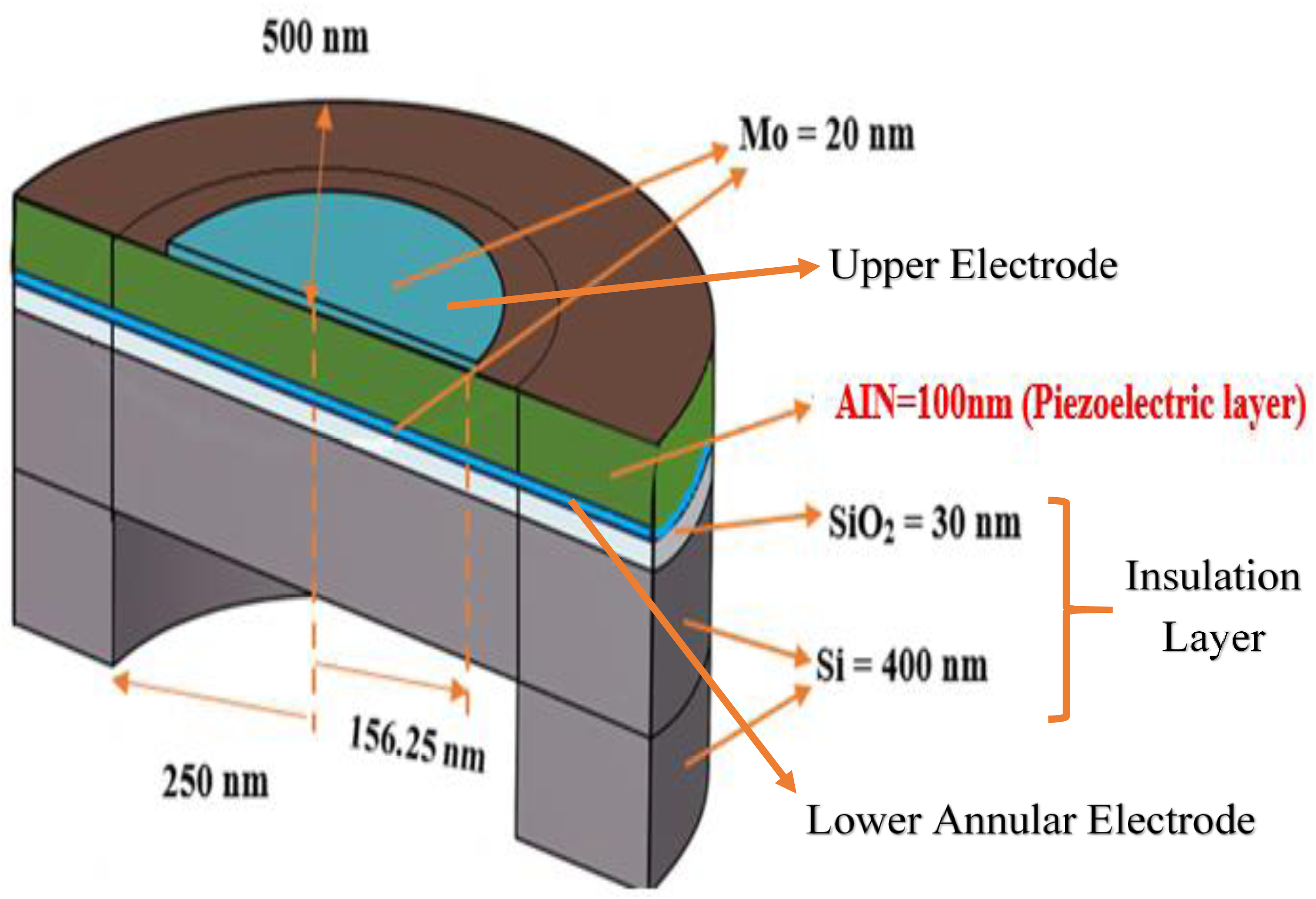
Schematic view of the proposed PMUT design.
The electrochemical coupling coefficient of the design is calculated using the following equations, the 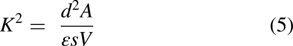
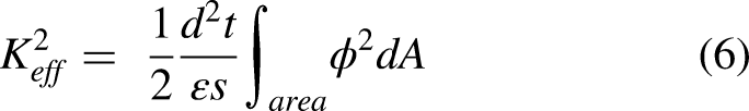
The frequency of the proposed PMUT design is obtained from the physical and dimensional properties of the diaphragm, which is given in the below equation,
23
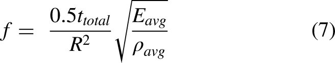
The layer thicknesses are as follows: electrode 20 nm, piezoelectric film 100 nm, insulator 30 nm, and silicon substrate 400 nm. This lamination maintains structural integrity while maximizing strain within the active region. The thickness of AlN in the model is larger than the thickness of the diaphragm, which ensures that the deformation of the piezoelectric material is more dominant than deformation other layers. The thin electrode present in the design minimizes the stiffness of the model as well as reduces the heavy load on the framework. The proposed design of PMUT achieves a resonant frequency of 18.883 MHz and a bandwidth of 10 MHz with high central displacement and bidirectional operation. These features make the proposed design an ideal framework for implantable and wearable biomedical ultrasonic system.
The structural parameters of the proposed design strongly influence performance and behaviour of the model. With a reduced diaphragm radius of 500 nm, bending stiffness of the model is lowered, which helps it an effective transfer of stress across the structure and increases the electrochemical coupling effect. The presence of partial electrode configuration with the size of the top electrode being adjusted with respect to the size of the bottom electrode, concentrates the electric field at the centre of the diaphragm, which suppresses higher order vibrations. The thickness of each layer ensures a balanced structure with enhanced electrochemical coupling, sensitivity and resonance frequency. The reduced diameter of the diaphragm increases the sensitivity of the model and optimizes the resonance frequency of the model.
Result and discussion
The results of the proposed nano-scale double-lamination AlN-based PMUT design are presented in this section. When the suggested PMUT was compared to various existing transducer designs, the outcomes showed that the proposed design improved the performance of sensors.
Experimental setup
The proposed PMUT design was implemented and simulated using the COMSOL software. The experimental setup specifications are as follows:

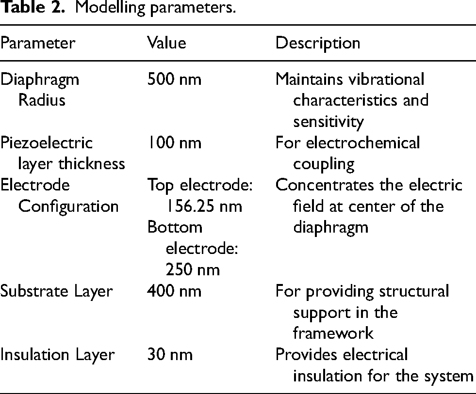
Modelling parameters
The modelling parameters of the proposed AlN based PMUT design are selected in a way to maintain strong electrochemical performance at nano-scale level. The parameters of the design are mentioned in the Table 2, which contains the parameter, the value of the respective parameter and a small description regarding the parameter in the framework.
Modelling parameters.
Simulated results of nanoscale AlN-based PMUT
The dynamic behavior of the proposed nanoscale PMUT was evaluated through COMSOL Multiphysics simulations to assess stress distribution, diaphragm displacement, electric potential, and electric field response during one vibration cycle.
A mesh image of the defined nanoscale AlN-based PMUT is illustrated in Figure 2. The geometry is a circular, multi-layered diaphragm structure, with the outermost boundary of 500 nm radius in the device. The mesh is composed of tetrahedral elements, a standard choice for discretizing complex 3D geometries in Finite Element Analysis (FEA). This refined meshing ensures computational accuracy in these critical regions of maximum displacement and mechanical constraint. The model contains about 12,700 elements with an average mesh quality of 0.48, which provides reliable simulation accuracy. This carefully constructed mesh forms the foundation for the subsequent high-fidelity multiphysics simulations performed in COMSOL. This structure contains a diaphragm radius of 500 nm with an AlN piezoelectric layer of 100 nm thickness, which helps in effective electrochemical reaction. The transducer achieves a resonant frequency of 18.883 MHz and bandwidth of 10 MHz makes it suitable for high frequency applications.
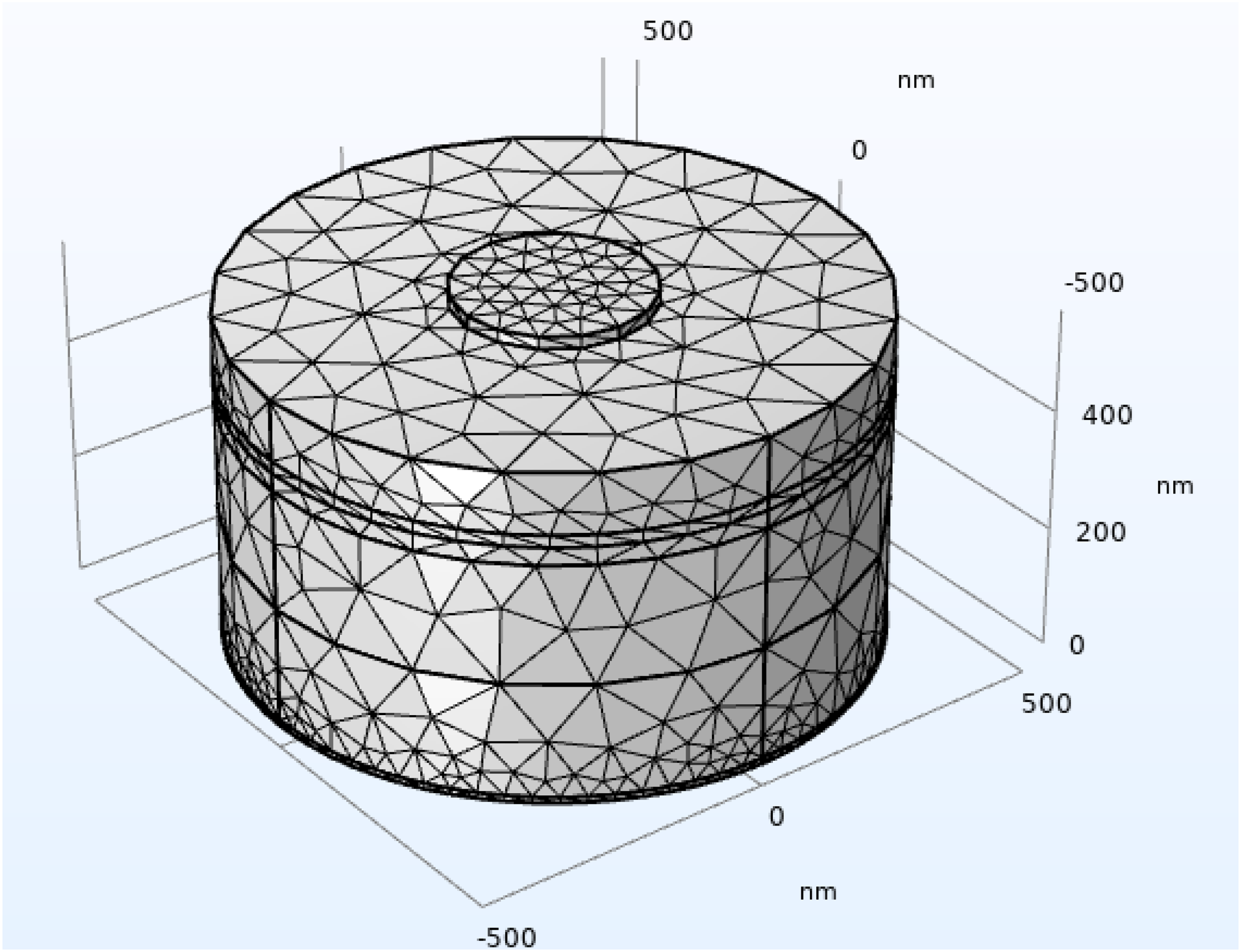
Mesh image of nanoscale AlN-based PMUT.
At three distinct time periods, Figure 3 illustrates how the Von Mises stress range in the nanoscale PMUT device behaves, (a) t = 0 s, (b) t = 0.1 s, and (c) t = 0.2 s. Initially at t = 0 s, von Mises stress is concentrated in the central region of the PMUT diaphragm (electrode layer), reaching the greatest levels of stress near 7 × 10⁵ N/m2. At t = 0.1 s, the stress is further intensified at 5.3 × 10⁵ N/m2 and spreads more prominently around the electrode edges and diaphragm center, reaching 1.9 × 10⁶ N/m2 in the piezoelectric layer. The stress spread relatively uniformly across the diaphragm, showing a successful energy transmission from the piezoelectric layer to the structure surrounding it. By t = 0.2 s, the stress begins to reduce and distribute more uniformly across the diaphragm surface, suggesting relaxation or transition into subsequent vibration cycles. The changes in Von Mises stress illustrate the dynamic mechanical response of the layered diaphragm structure under electrical excitation, highlighting areas susceptible to mechanical loading and potential fatigue. The indicated stress changes with time confirm that the design of the device dissipates stress while enabling stable nano-scale actuation.
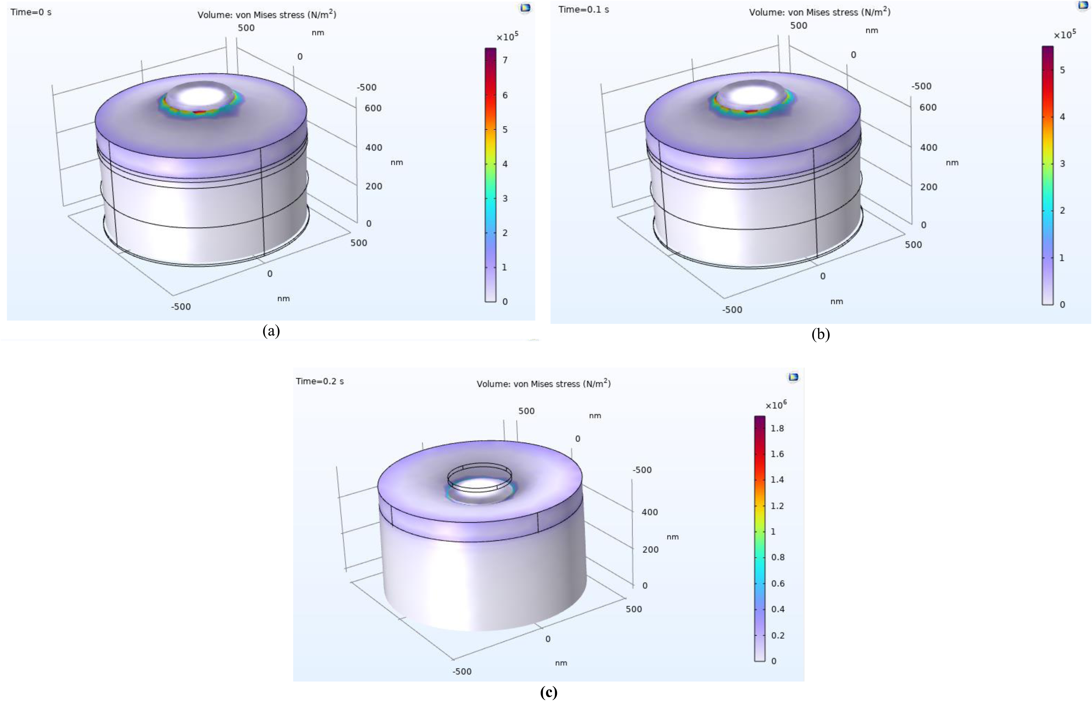
Von Mises stress in (a) t = 0 s, (b) t = 0.1 s, (c) t = 0.2s.
Evolution of displacement magnitude with varied time of proposed PMUT diaphragm is presented in Figure 4. At t = 0 s, maximum displacement is found closer to the top electrode with a value of 2.4 × 10⁻⁴ nm, and peripheral areas are almost stationary, thereby validating that deformation is localized at the diaphragm center. At t = 0.1 s, the diaphragm displacement is noticeably enlarged to a peak value of 16.7 × 10⁻⁵ nm. The distribution of the displacement shows a regular radial gradient from the center to the edge, reflecting effective out-of-plane deflection with little structural distortion. The high-intensity central area (red region) reflects strong electromechanical coupling and effective strain transfer from the AlN film onto the diaphragm surface. At t = 0.2 s, the central displacement reaches 6 × 10⁻⁴ nm, demonstrating the uniform vibration evolution. The homogeneous displacement gradient proves minimal structural deformation during actuation. The outcomes prove increased central sensitivity and sound output.
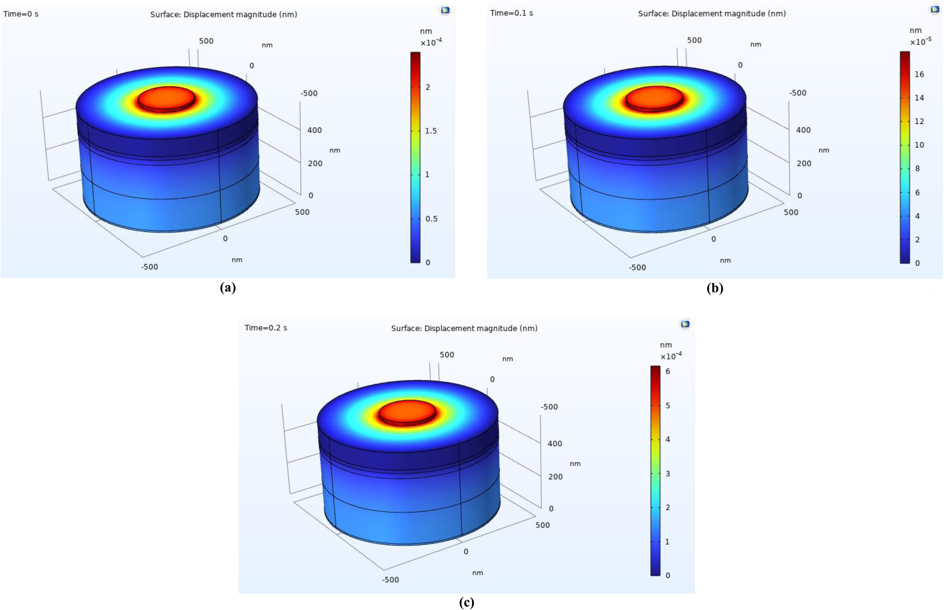
Proposed PMUT's displacement norm at (a) t = 0 s, (b) t = 0.1 s, (c) t = 0.2 s, where upper arrow indicates maximum electric potential while lower arrow for minimum.
The electric potential distribution of the PMUT during one vibration cycle is illustrated in Figure 5. At t = 0 s, the initial electric potential is applied, establishing the baseline field. The concentration of potential is extremely concentrated under the top central electrode and has a maximum value of 4.29 × 10⁻⁵ V. The distribution is axisymmetric and decays very quickly toward the clamped edge of the diaphragm, verifying that the electric field is effectively confined in the active center region by the partial electrode design. At t = 0.1 s, during actuation, there is an intense negative potential of 3.3 V appears at the center, showing the reverse piezoelectric effect as mechanical strain causes voltage reversal. The sharp potential gradient shows high strain at the center of the diaphragm, which corresponds to maximum displacement. At t = 0.2 s, the polarity of the potential is reversed to 0 V, showing harmonic oscillation of the diaphragm, and the electric potential field is inversely coupled with the cyclical mechanical strain. Axisymmetric contours and lack of irregular field nodes provide evidence of higher-order vibration mode suppression. This verifies that partial electrode geometry increases central actuation efficiency and fundamental mode dominance.
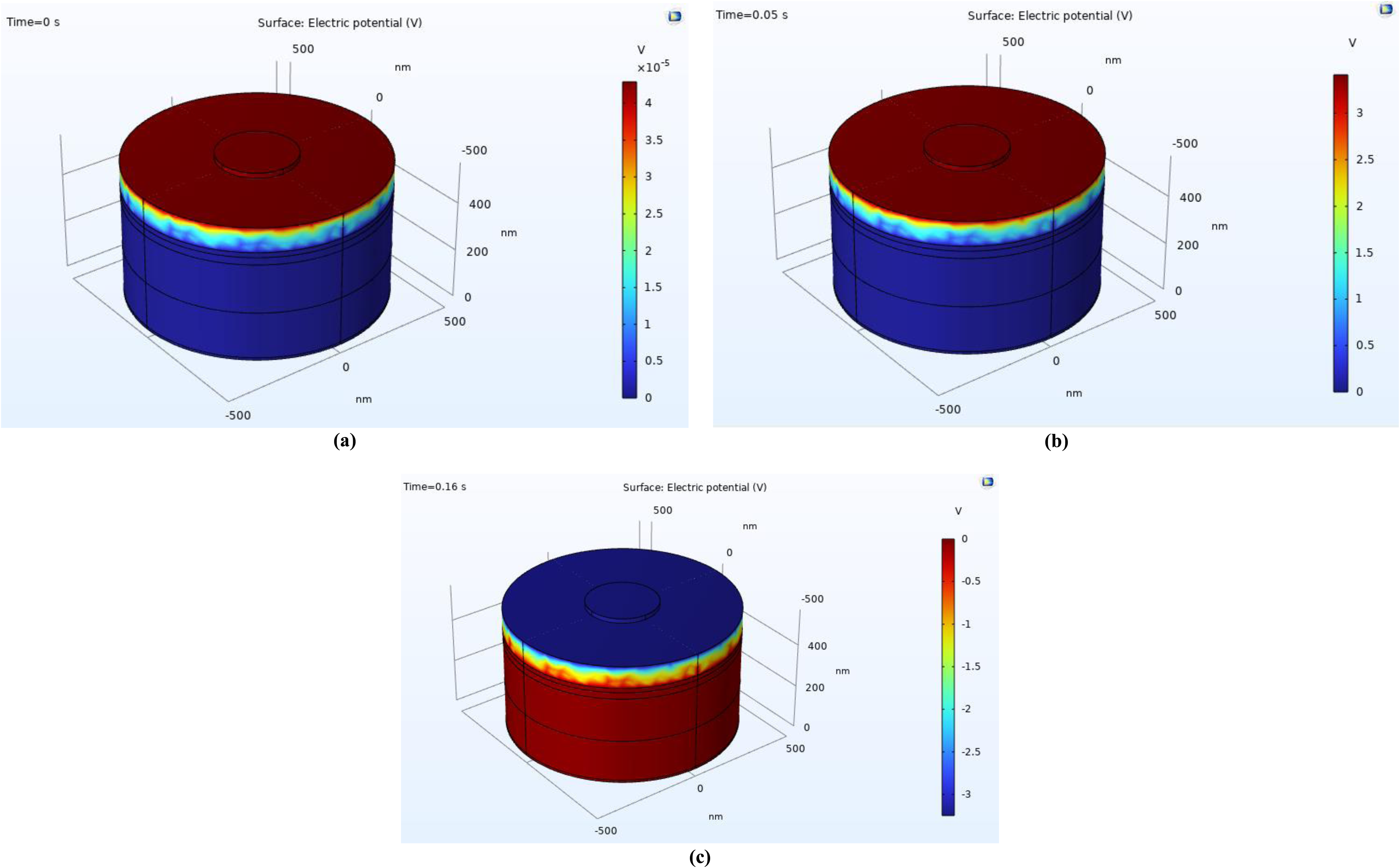
Proposed PMUT's electric potential at (a) t = 0 s, (b) t = 0.1 s, (c) t = 0.2 s where upper arrow indicates maximum electric field norm while lower arrow for minimum.
The electric field norm behavior of the proposed nano-scale AlN PMUT is illustrated in Figure 6 within one vibration cycle. When voltage is applied at t = 0 s, a localized electric field is generated under the central top electrode with a value of about 4.92 × 10³ V/m, which decreases radially towards the clamped edge. This axisymmetric concentration is due to the partial electrode structure, which localizes the potential in the central active area to create efficient actuation. At t = 0.1 s, it has its highest strain rate, and high piezoelectric coupling maximizes the field to 3.6 × 10³ V/m, indicating the active interaction between mechanical deformation and induced polarization. The electric field pattern becomes more distributed yet remains axisymmetric around the center. At t = 0.2 s, the field is stabilized with a maximum of 12.2 × 10³ V/m, showing quasi-steady electromechanical equilibrium. The findings confirm that the optimized partial electrode design maximizes field localization and coupling strength.
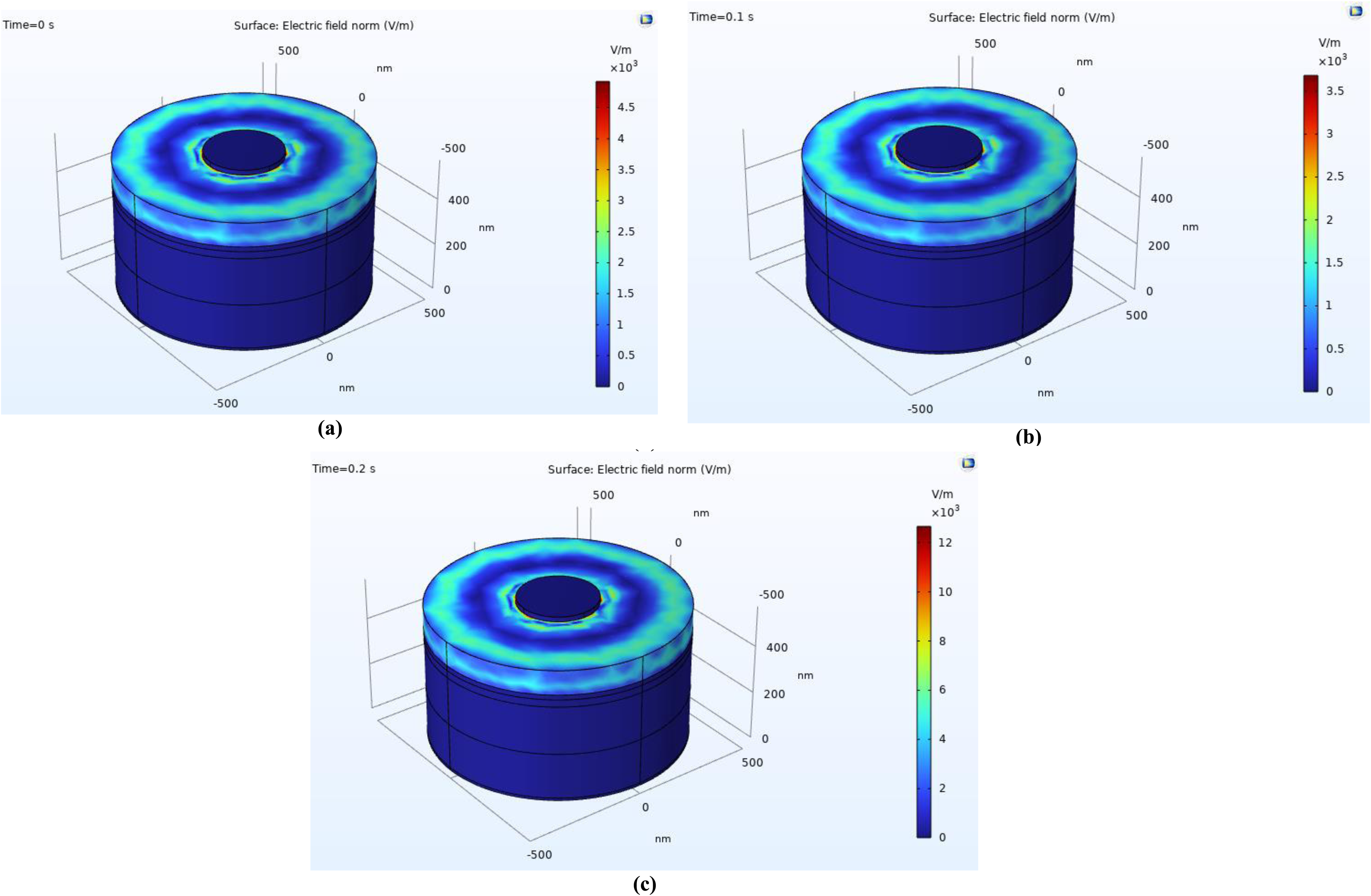
Proposed PMUT's electric field norm at (a) t = 0 s, (b) t = 0.1 s, (c) t = 0.2 s where upper arrow indicates maximum displacement norm while lower arrow for minimum.
Performance evaluation of the proposed PMUT design
This section offers a thorough description of results obtained and the effectiveness of the proposed PMUT design under the specified parameters, such as total electric energy, polarization norm, energy density, electric potential, electric field norm, total sound pressure level (SPL), thickness coupling coefficient, and normalized amplitude.
Figure 7 illustrates the performance of total electric energy depends on time. From the figure, it is noted that at times 0.05 s and 0.15 s, there is a maximum total electric energy of 3.3 × 10⁻¹⁴ J, which corresponds to the device's ability to convert mechanical energy into electrical energy. In between these two peaks, the energy drops to nearly zero, reflecting the overall cyclic nature of the piezoelectric response. This periodic response suggests that the electromechanical coupling between the diaphragm and piezoelectric layer is stable.
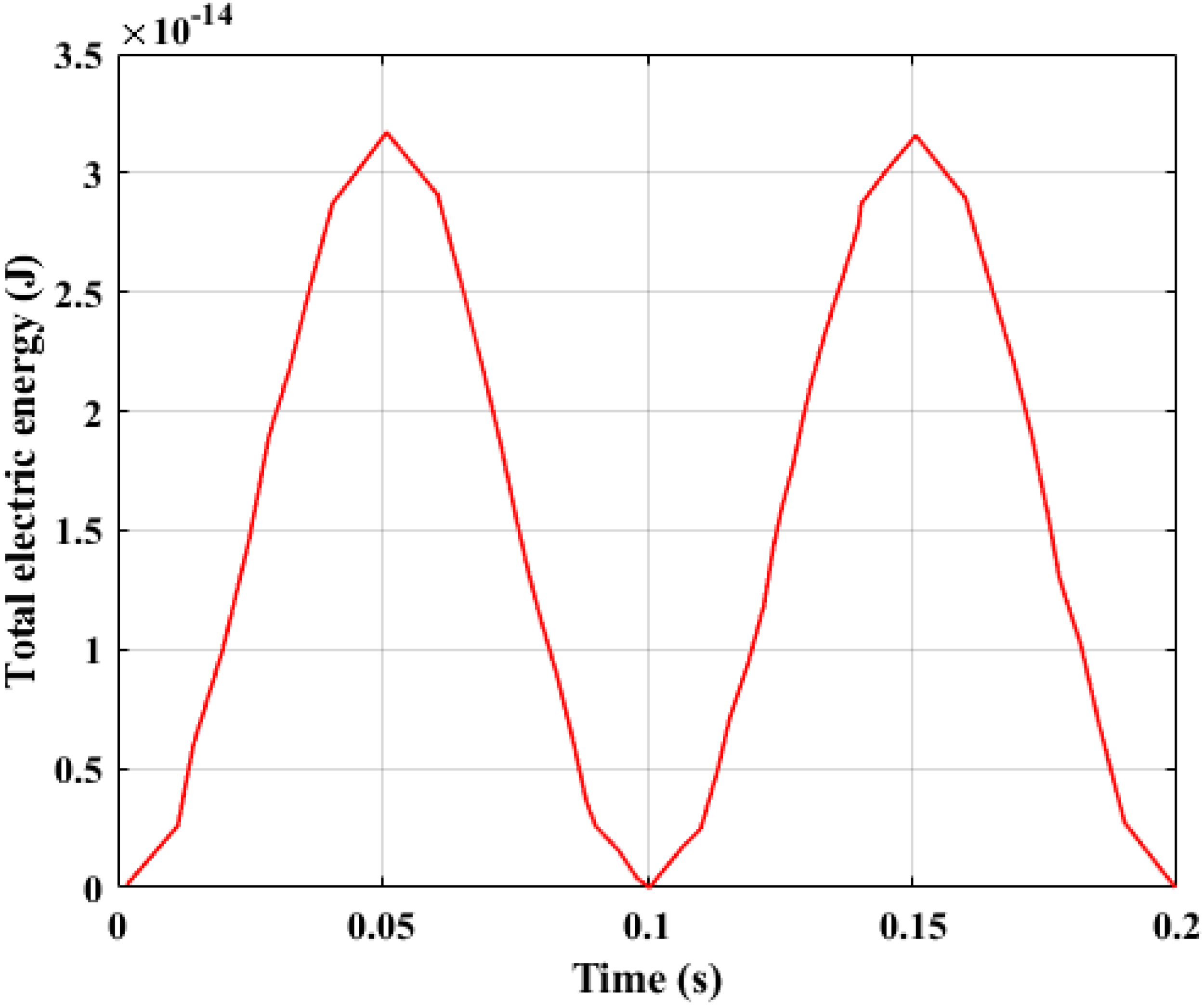
Total electric energy analyzation of the proposed PMUT design.
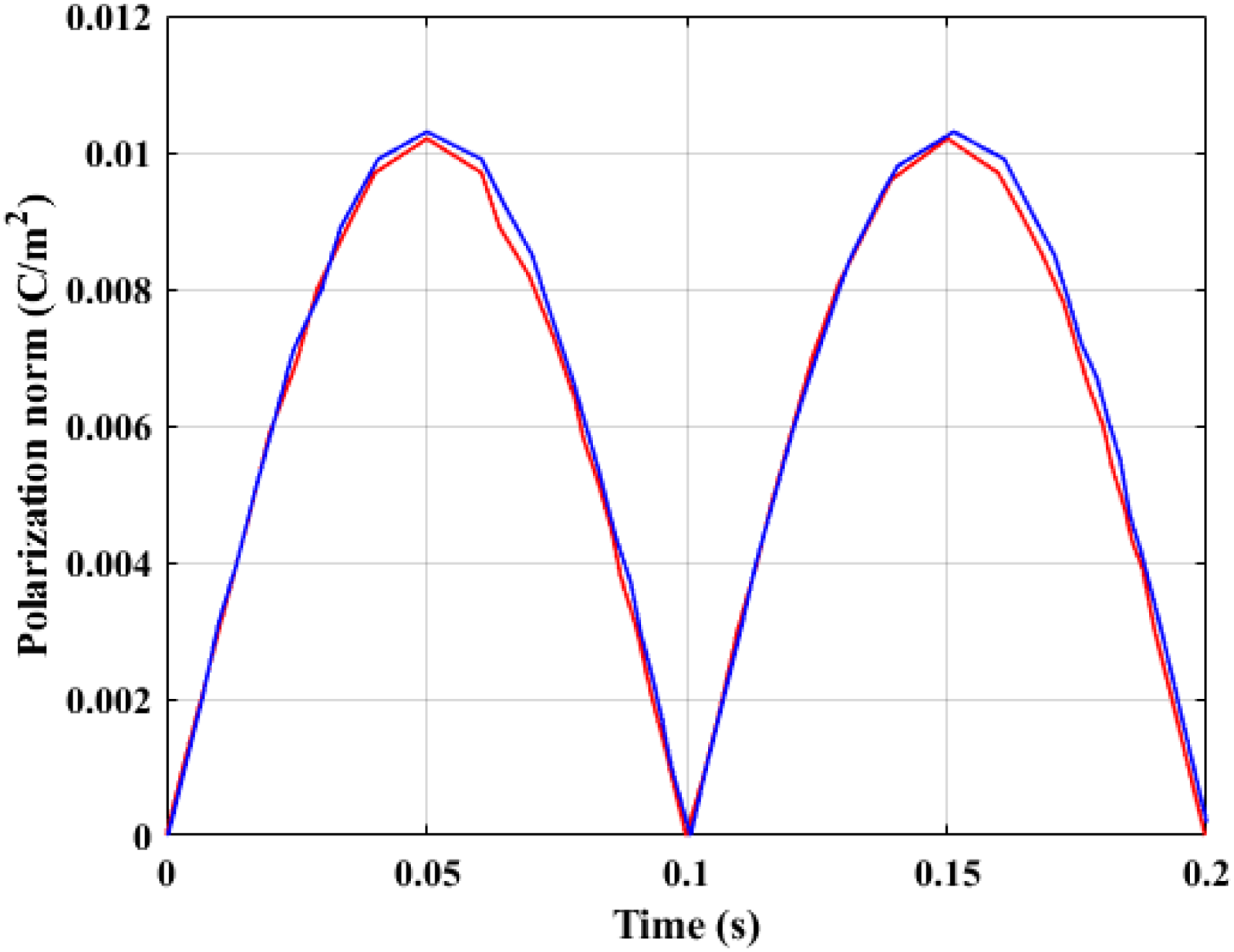
Polarization norm (in C/m2) of a piezoelectric layer over time (in seconds) along with its expermental validation is illustrated in Figure 8. Here, the polarization norm indicates the magnitude of the polarization vector, which indicates the strength of the conversion of mechanical enrgy into electrical energy. The polarization norm of the original design starts at a value close to 0 at time 0 s. It then increases rapidly, reaching a peak value of around 0.01 C/m2, at 0.05 s. The clear, sustained sinusoidal waveform indicates a stable and effective conversion of energy with very little damping or distortion, suggesting strong electromechanical coupling.
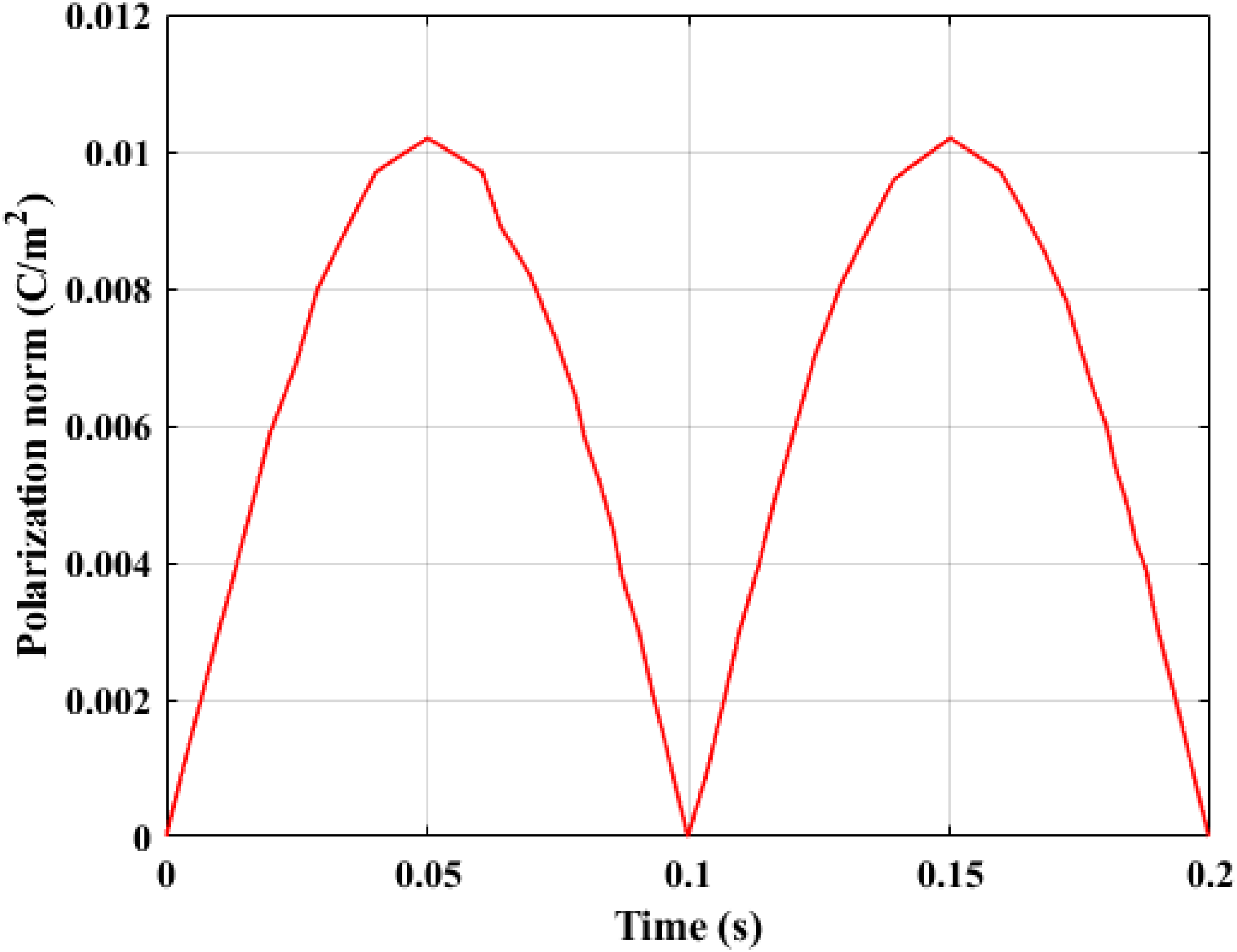
Polarization norm.
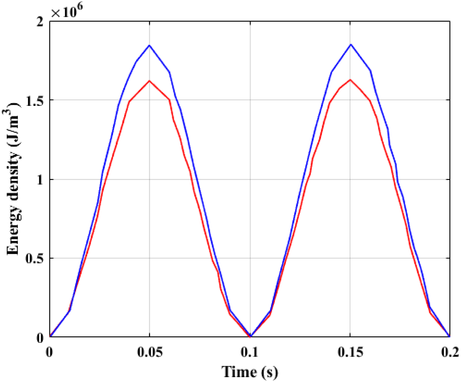
Figure 9 displays a periodic waveform representing energy density (J/m3) as a function of time (s). The energy density of the ideal design oscillates sinusoidally, reaching a peak value of 1.7 × 10⁶ J/m3 at 0.05 s and 0.15, which shows effective energy conversion at these intervals. The sinusoidal pattern reflects a predictable and repeatable mechanical response of the diaphragm. Minimal amplitude variation between cycles suggests low energy loss and high electromechanical efficiency.
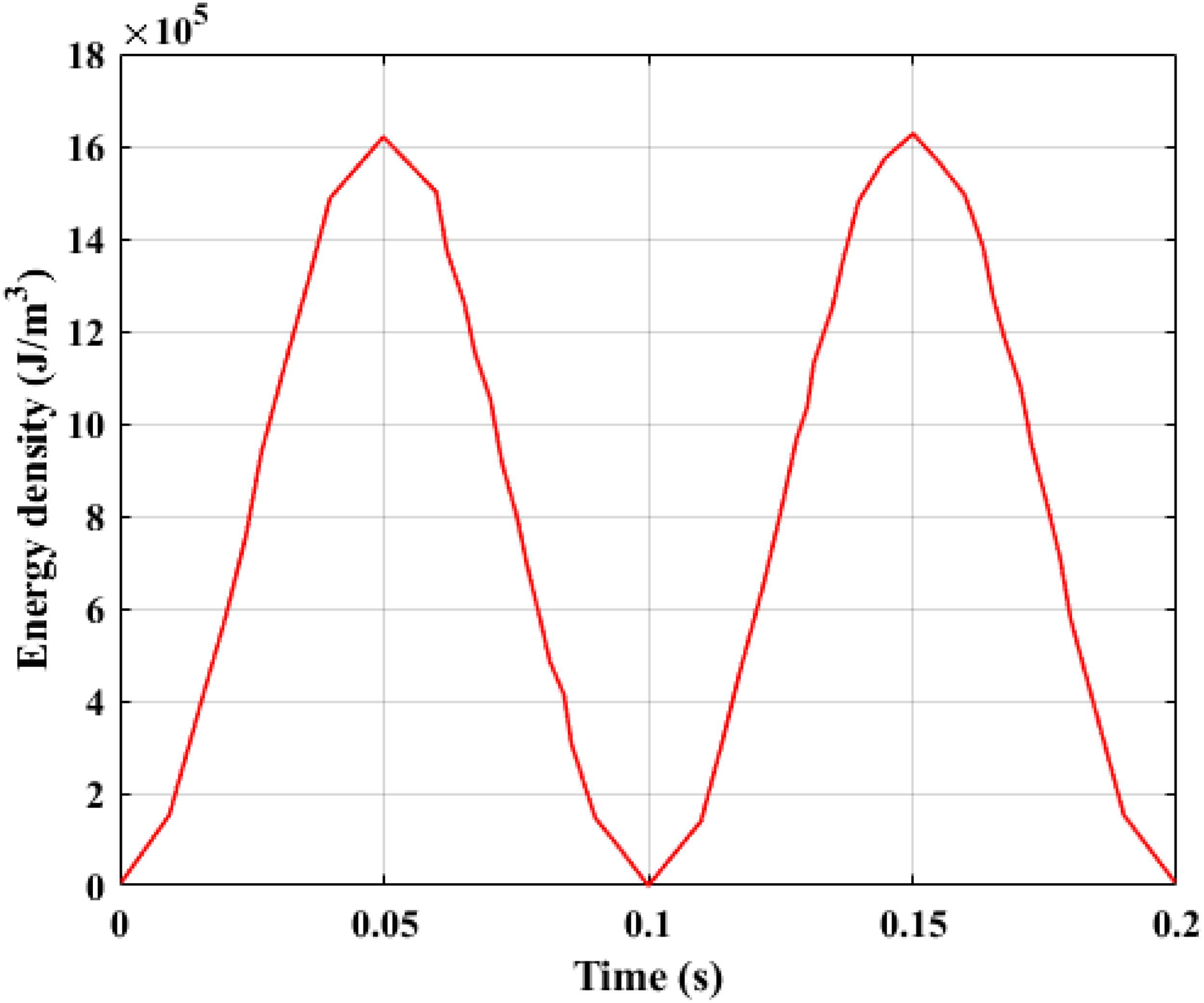
Performance of energy density.
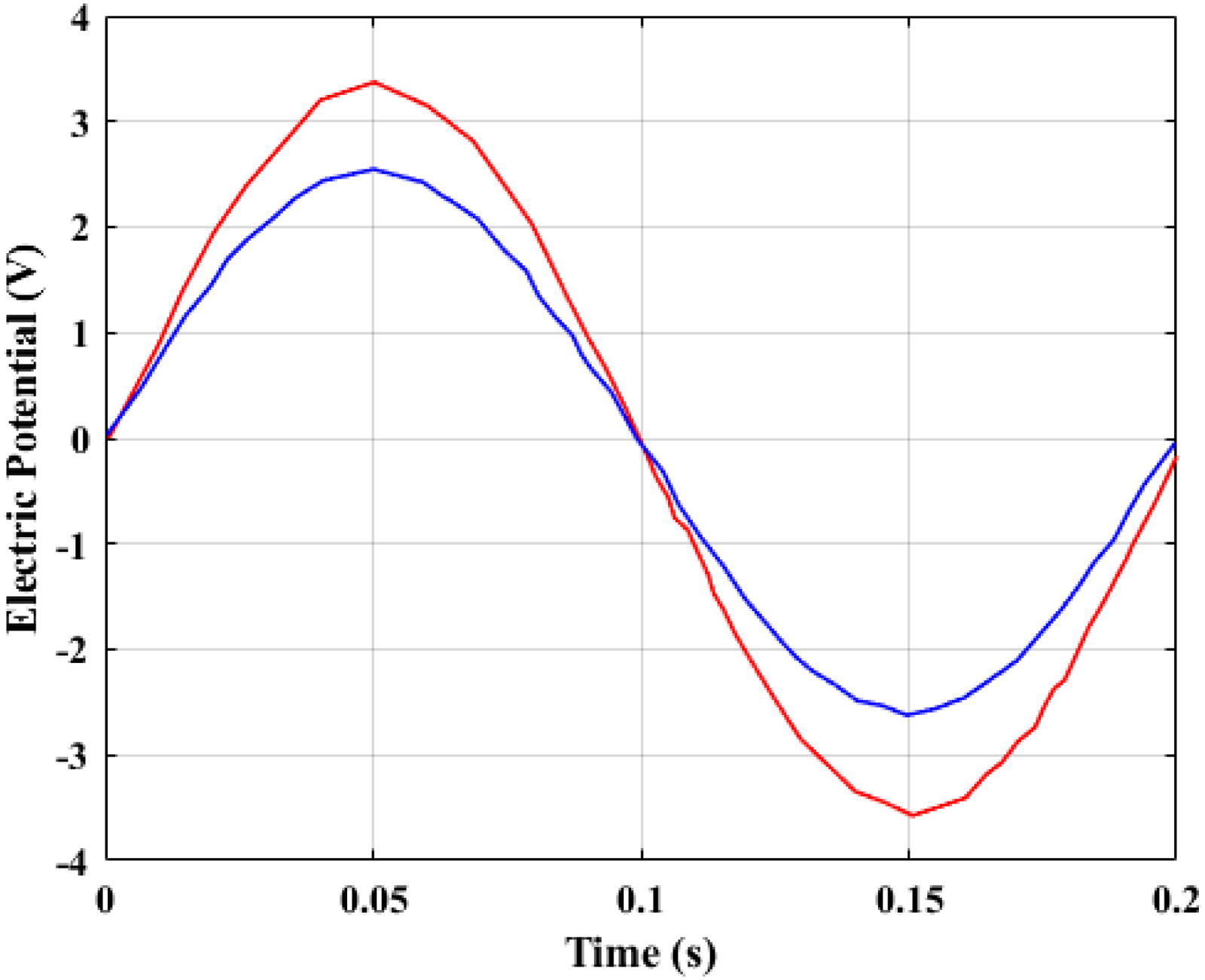
Figure 10 shows the electric potential developed over the piezoelectric layer as a function of time during the actuation process. In the ideal design, the sinusoidal response wave indicates that the electromechanical energy conversion is particularly efficient, as the mechanical vibrations of the diaphragm produce the electric potential response. Between time 0.05, the potential reaches its peak value of 3.3 V, which is the maximum instantaneous electric potential reached during a single cycle, the electric potential reaches a low of −3.3 V during 0.15 s, and during this point, there is no sign of nonlinear distortion and the diaphragm is still functioning efficiently. After reaching the peak potential, the generated electric potential gradually dissipates which is caused mainly by the energy dissipated through the elastic support layer and the surrounding fluid.
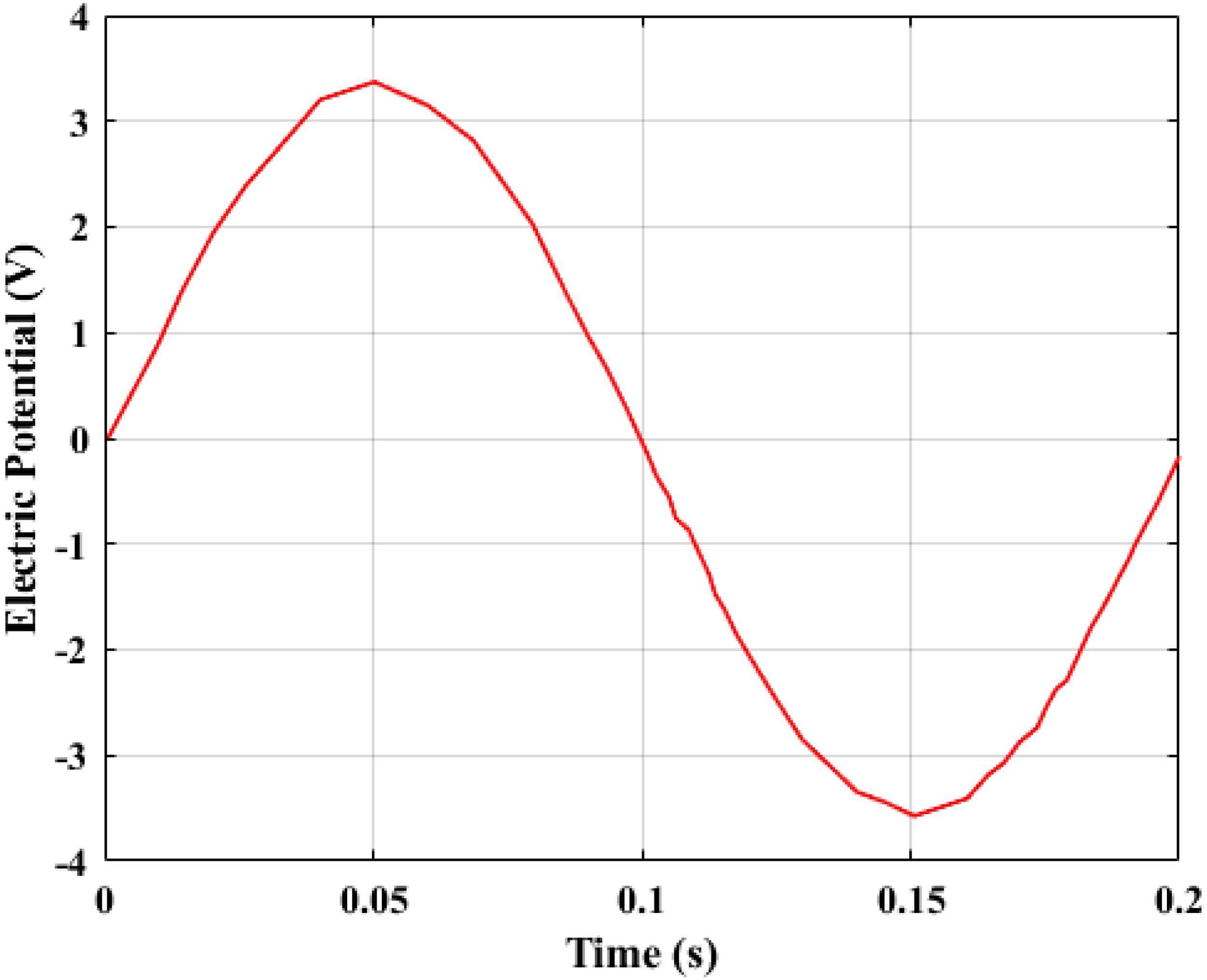
Time-dependent electric potential response of the proposed nano-scale PUMT diaphragm.
The electric field norm analysis of the proposed PUMT is shown in Figure 11. In here, to evaluate the robustness of the model in experimental design, a parameteric sensitivity analysis is performed in the model by making small variations in the input parameters. In real experimental small deviation occur in fabrication, so small adjutments are made in the design of the model and it is compared with the original model to determine its reliability in experimental design. In here, the red line indicates the ideal simulated proposed model and blue line indicates the proposed model with variability in parameter value.
Electric field norm analyzation of proposed PUMT.
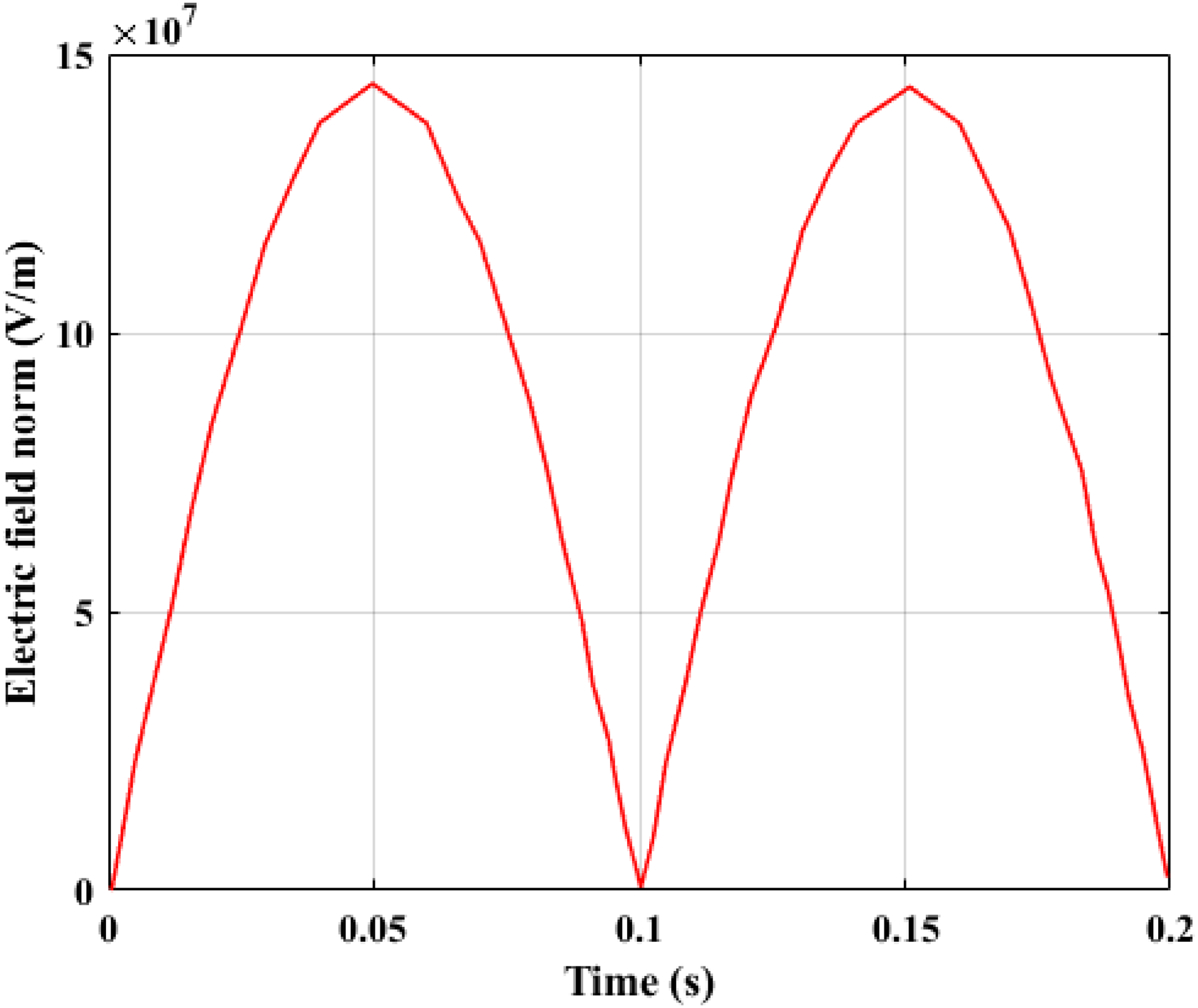
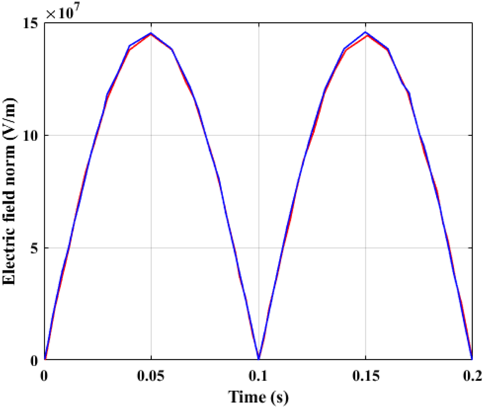
As noted from the figure, the proposed PMUT exhibits a rapid electrical response reaching an electric field norm maximum of 14.1 × 10⁷ V/m at 0.05 s and 0.15 s, representing a peak electromechanical action. As in times 0.1 s and 0.2 s, the electric field norm reaches zero, which reflects the expected natural oscillatory of the diaphragm. This variation in cyclic values represents a sufficient energy conversion between the electric and mechanical domains. The high peaks of the electric field in the early time instances suggest the possibility of fast actuation for high-frequency applications. Whereas, the altered desing reached a maximum electric filed norm of 14.1 × 10⁷ V/m at 0.05 s and 0.15 s and 0 at 0.1 s and 0.2 s, which is similar to original design and there is almost no variations in the value, which indicates the reliability in real time performance of the model.
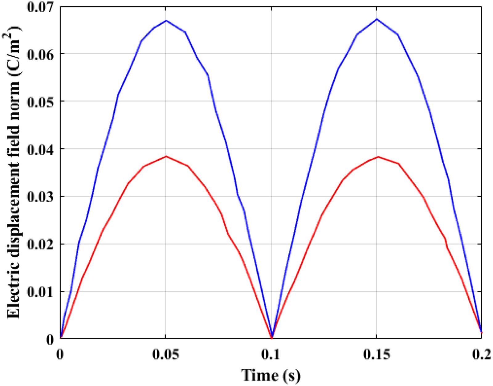
The performance of the electric displacement field norm of the proposed work is shown in Figure 12. The proposed nano-scale PMUT shows good electromechanical performance, with an electric displacement field reaching a peak of 0.067 c/m2 at 0.05 s and 0.15 s. Transient behavior illustrates consistent peak stays at multiple times, which demonstrates stable dynamic performance. This shows that it transduces dynamically at a fast and effective rate, sustainable for high frequency for both ultrasound applications.
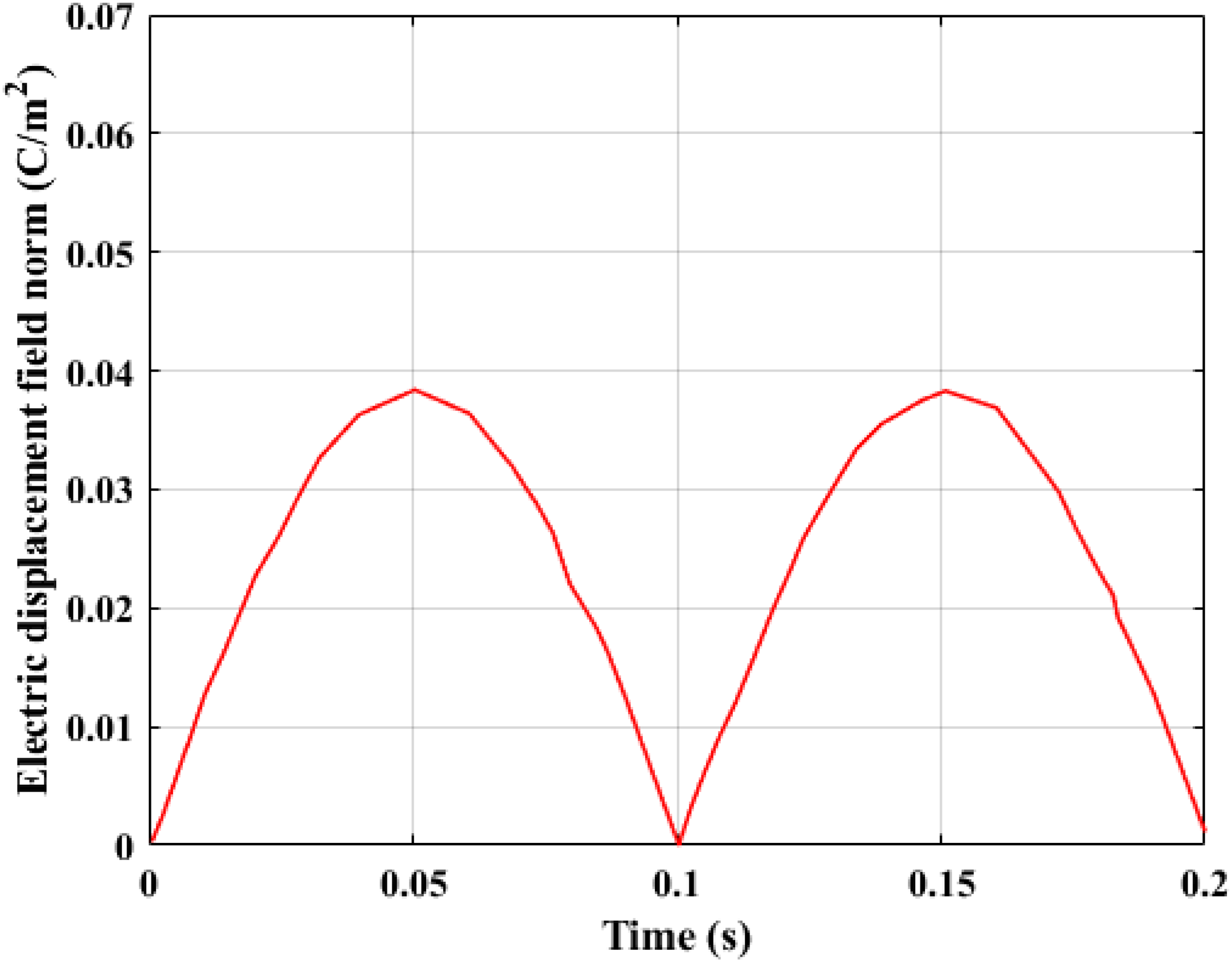
Electric displacement field norm performance analyzation.
Figure 13 shows the variation of total sound pressure level (SPL) as a function of diaphragm radius in the proposed PMUT design. SPL increases steadily as the radius grows, reaching a peak of approximately 2.59 × 10⁻⁵ pa at 150 nm radius, which corresponds to the region of maximum piezoelectric-induced displacement. Beyond 150 nm, the SPL drops sharply to near 2.00023 × 10⁻⁵ pa at 200–300 nm radius, showing reduced contribution from the outer diaphragm region. From 300 nm to 500 nm, the SPL remains low but slightly increases to around 2.08 × 10⁻⁵ pa, reflecting minor contributions from the peripheral diaphragm area. This behavior highlights that the central region of the diaphragm dominates acoustic generation, and partial electrode placement targeting this zone effectively maximizes sound pressure while suppressing higher-order vibrations in the outer areas.
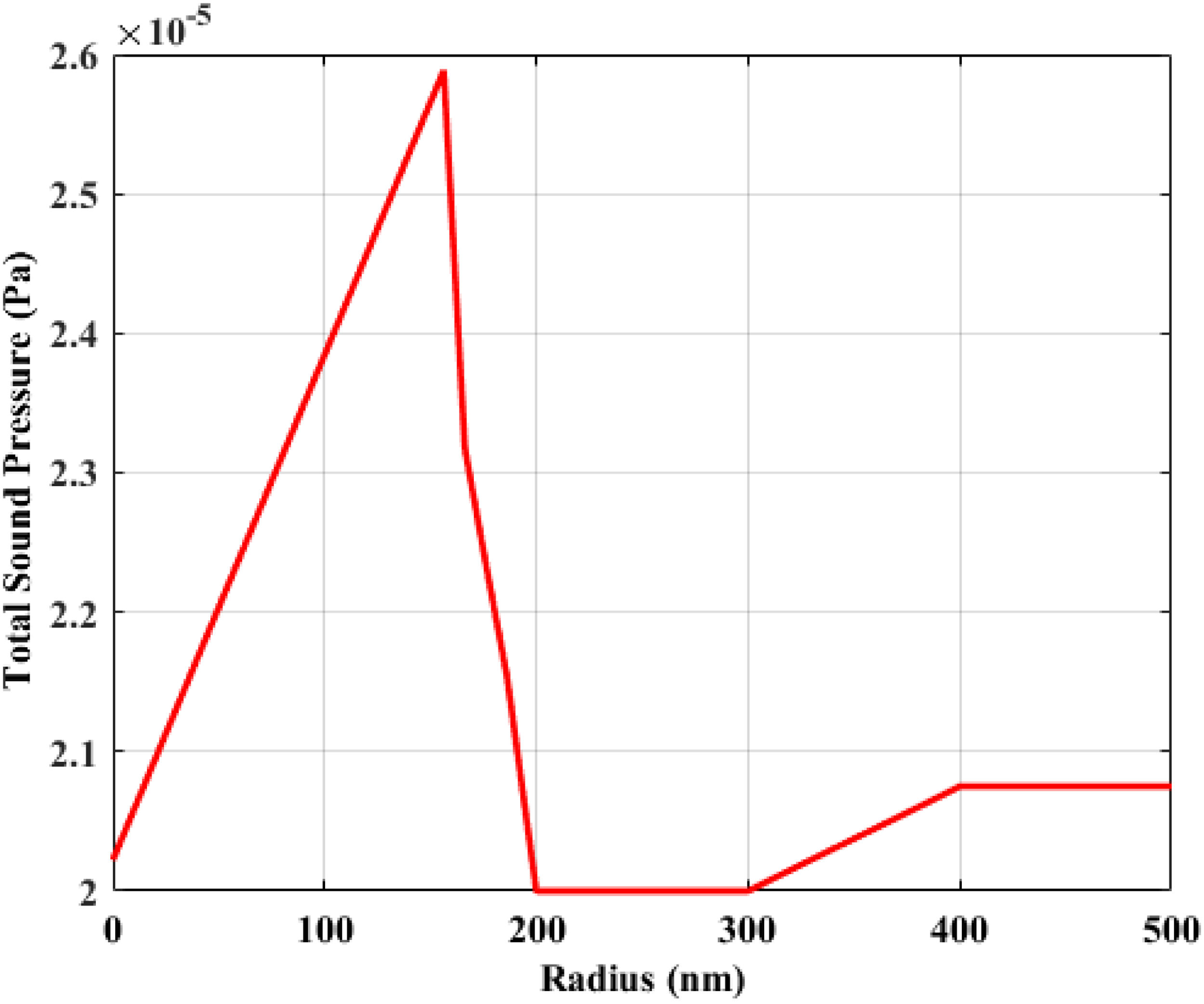
Total SPL of the proposed PMUT design.
Figure 14 illustrates the inverse relationship between diaphragm thickness and the objective performance parameter of the proposed PMUT. The objective performance parameter evaluates the efficiency of the PMUT design in achieving strong electrochemical coupling and better displacement. As the thickness of the diaphragm transitions from 10 nm to 1000 nm, a rapid decrease in objective value is observed from approximately 15 × 105 to below 0.01 × 10⁵. This indicates the importance of diaphragm stiffness on PMUT efficiency: thinner diaphragms enable the piezoelectric layer to deform more easily, thus promoting strain transfer, whereas thicker diaphragms increase mechanical stiffness, thereby reducing diaphragm displacement and the transduction efficiency significantly.
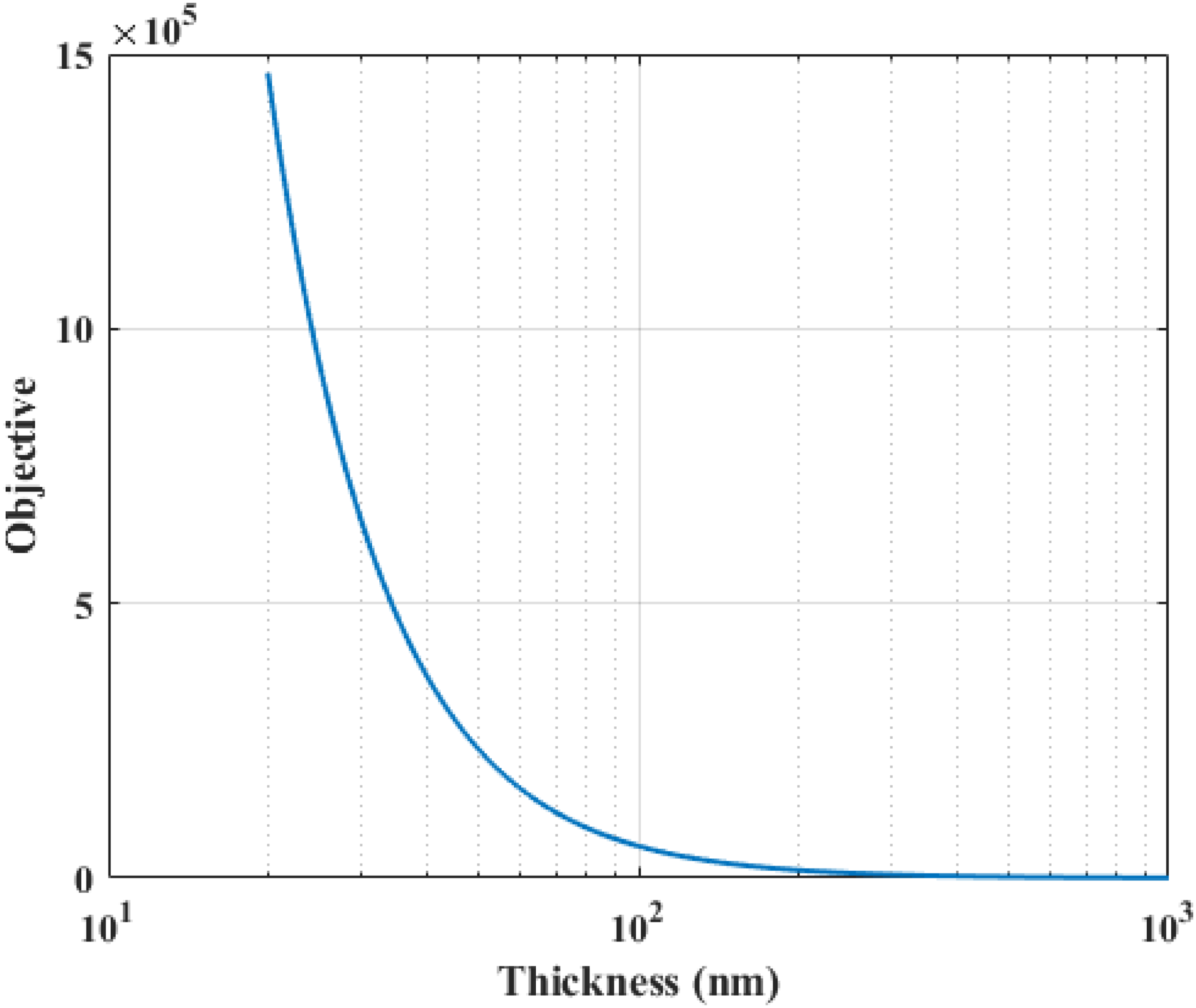
Diaphragm thickness and the objective performance parameter.
Figure 15 shows the thickness coupling coefficient (
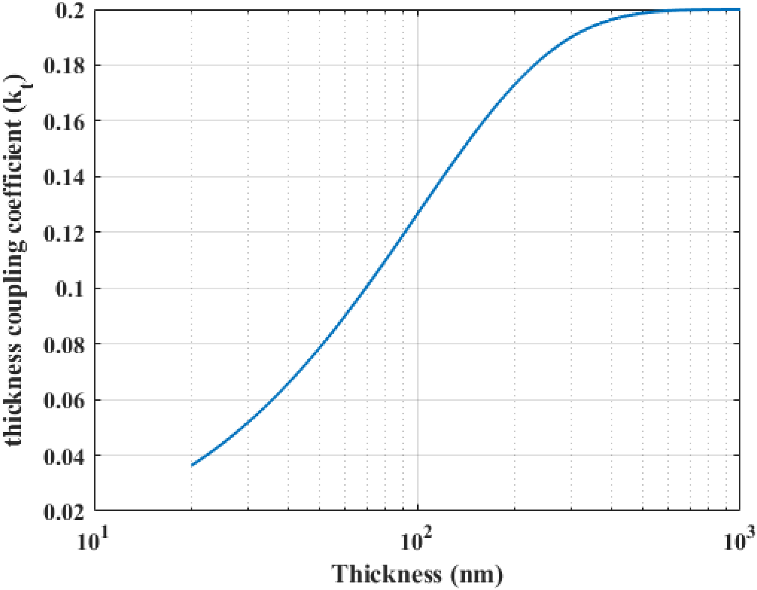
Thickness coupling coefficient vs thickness analyzation.
The relationship between Bandwidth, Diaphragm Length, and Thickness is illustrated in Figure 16. As diaphragm length increases, the maximum achievable bandwidth significantly decreases, and this decrease is further influenced by increasing thickness. For small diaphragm lengths (10 μm) and small thickness (200 nm), the bandwidth is highest, approaching about 50 MHz. PMUT design with a 500 nm radius diaphragm and 100 nm thick AlN layer fits within the optimal region on this graph, enabling a high bandwidth of 10 MHz observed.
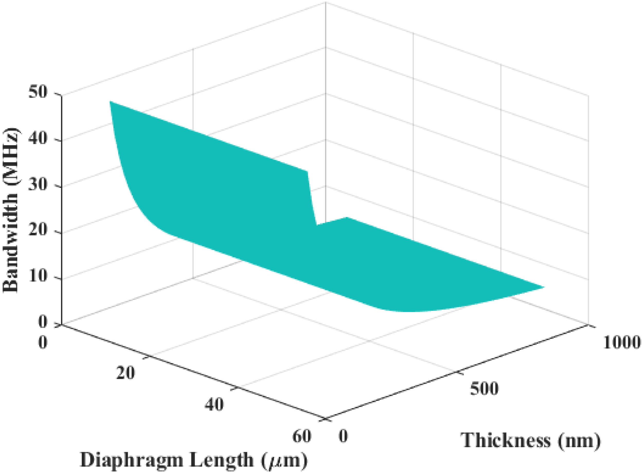
Relationship between bandwidth, diaphragm length, and thickness.
For the suggested PMUT design, Figure 17 illustrates the inverse relationship between diaphragm thickness and bandwidth. The bandwidth drops from roughly 105 kHz to 104 kHz as the thickness rises from about 10 nm to roughly 1000 nm. In particular, the bandwidth decreases to about 10 kHz at a thickness of 1000 nm, while it reaches its maximum value close to 2 × 10⁵ kHz at a thickness of 20 nm. This pattern suggests that a wider frequency response is made possible by thinner diaphragms, which is essential for improving PMUT performance, particularly in applications such as nanoscale biomedical devices.
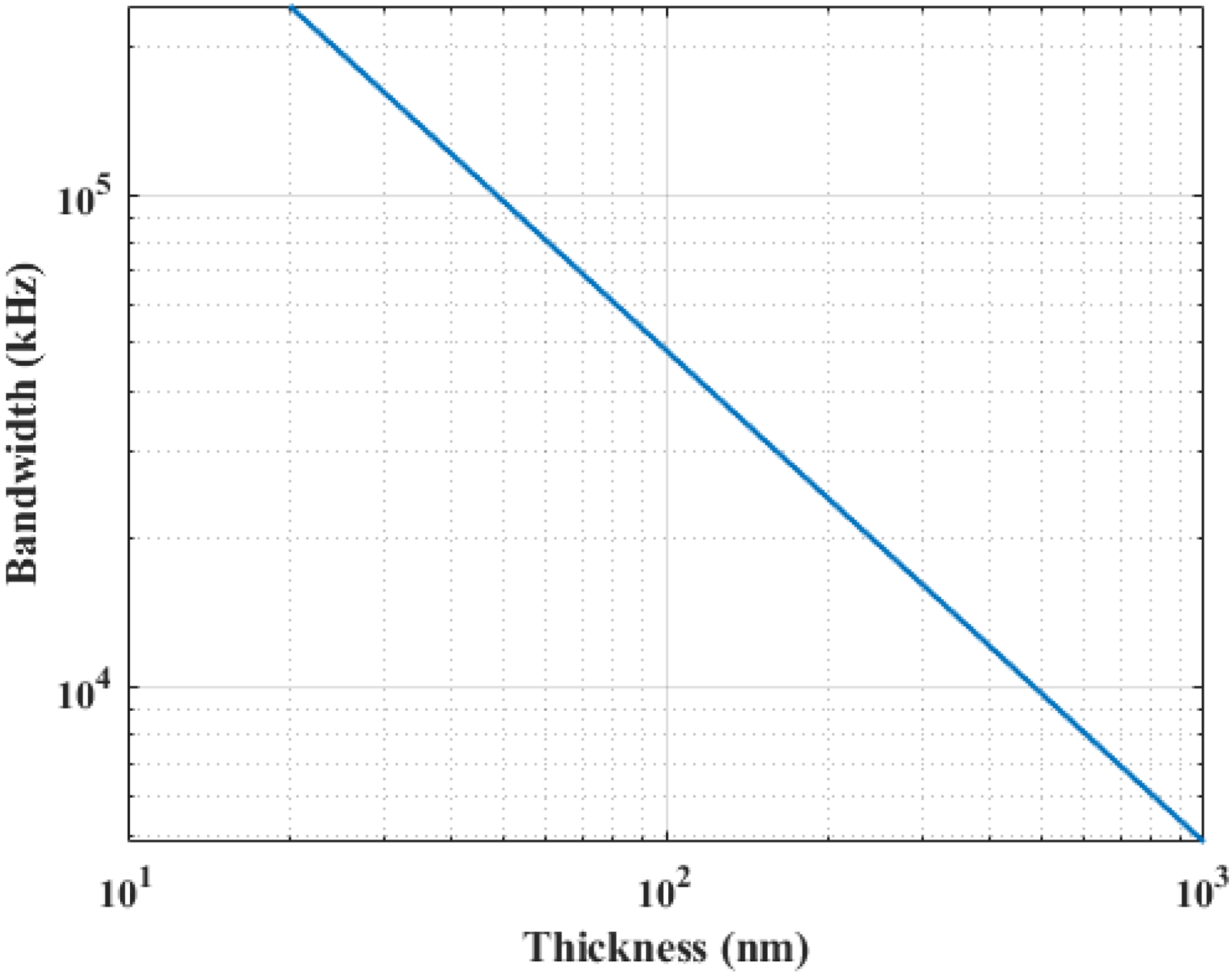
Bandwidth vs thickness.
The frequency response and resonance parameters for the suggested nano-scale PMUT design are illustrated in Figure 18. The device demonstrates sharp behavior at approximately 18.833 MHz, achieving a normalized amplitude of 1.0, which is the primary resonant frequency of the system. The plot reveals a sharp resonance peak, demonstrating excellent electromechanical coupling efficiency at this frequency, which is crucial for high-performance ultrasonic sensing. Additionally, side lobes are present at frequencies lower and higher than the primary peak (about 18.75 MHz and 18.9 MHz) corresponding to higher-order resonant modes, but their amplitude is much smaller.
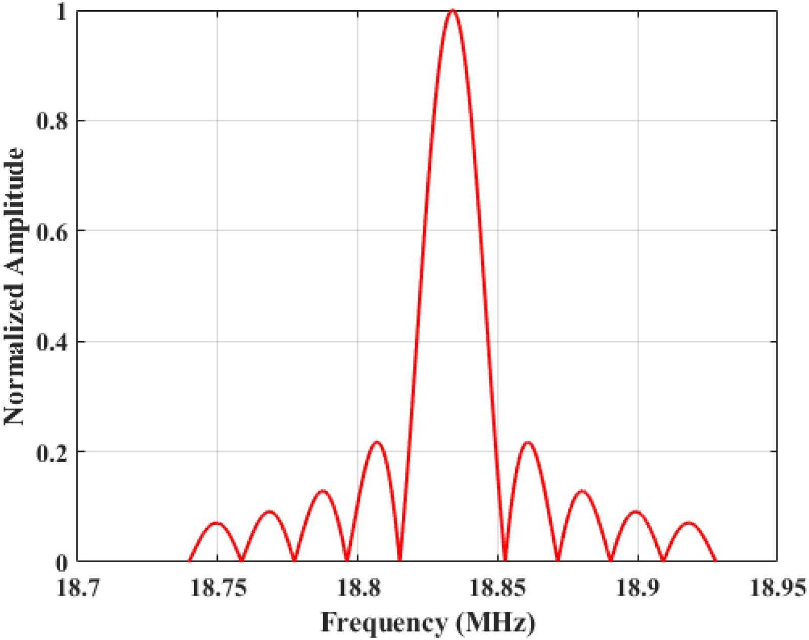
Normalized amplitude vs frequency.
The insertion loss is the loss in the signal of the model in the acoustic model of the PMUT, which is shown in the Figure 19. The insertion loss reaches 0 db at 100 MHz, indicating efficient signal transmission, which represents the conversion of electrical energy of the device with minimal loss. The AlN provides strong piezoelectric coupling, low dielectric loss and high thermal stability, with this the proposed design achieved better transmission efficiency and lower energy loss.
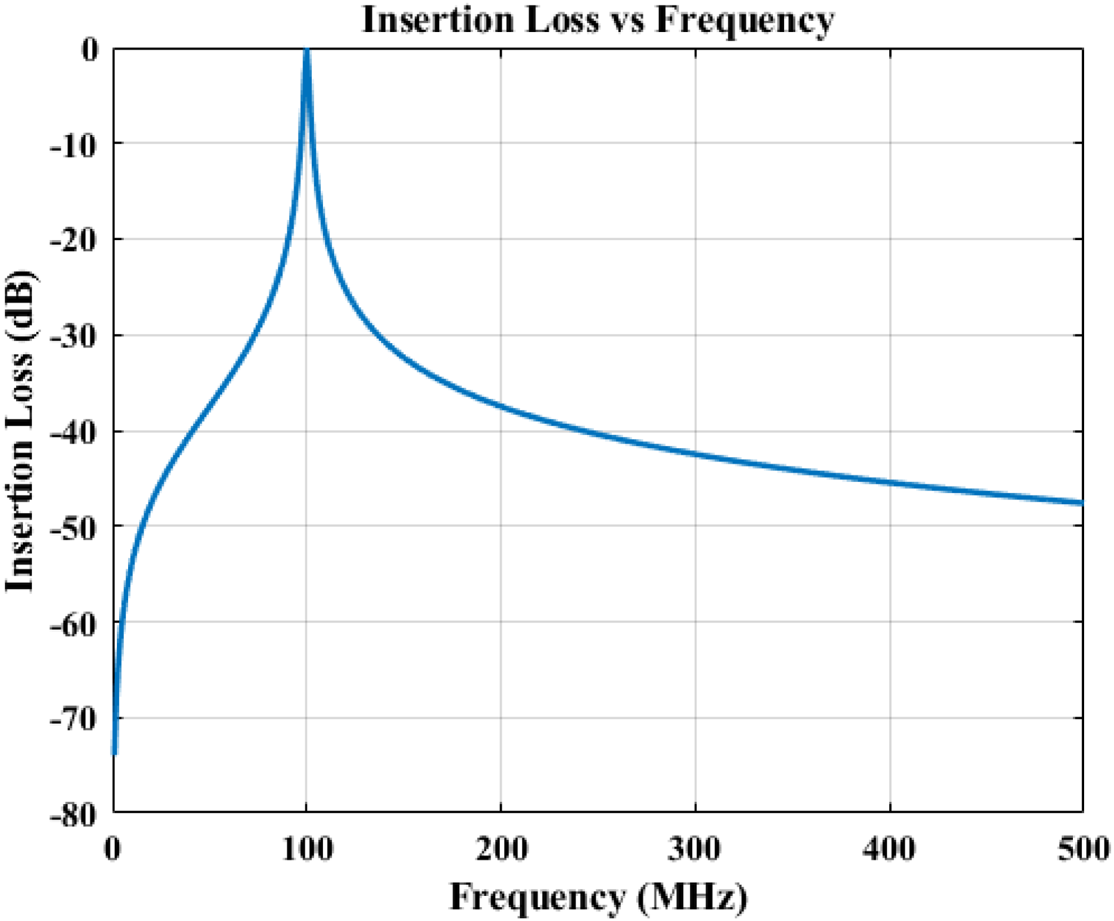
Insertion loss as a function.
Stability against depolarization indicates the ability of a piezoelectric material to maintain its polarization and functional performance at increased depolarization effect, which is represented in Figure 20. In this, the blue line indicates exponential decay and orange line indicates nonlinear residual model, where the nonlinear residual model maintains higher stability compared to the rapid decay shown by the exponential model. This indicates the ability of the material to not lose its polarization quickly and to retain a stable state, ensuring better reliability and performance of the model.
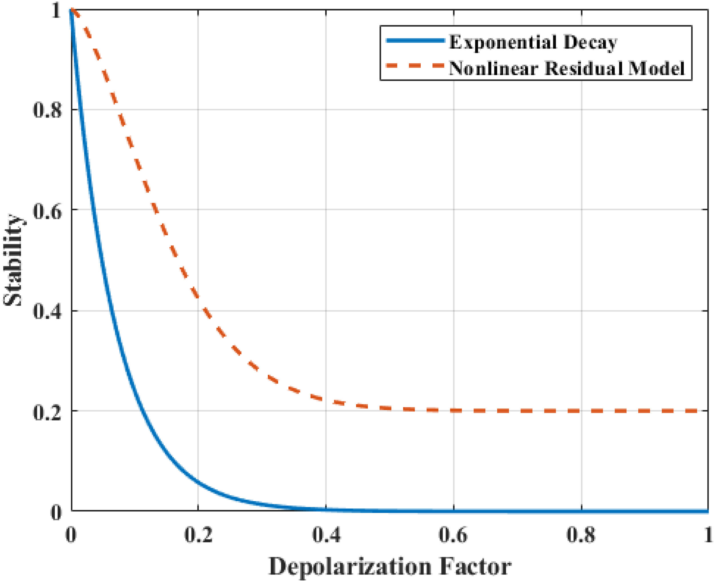
Stability against depolarization.
Figure 21 represents the electric fatigue, which represents the gradual degradation of piezoelectric performance when the device undergoes repeated electrical excitation cycles. In the figure, it is clear that the model maintains the normalized stability near 1 for a long period of time, which indicates the long-term performance of the material in maintaining its polarization and functional properties. There is a sudden degradation in the curve at around 107 cycles, which indicates the strong fatigue resistance of the system.
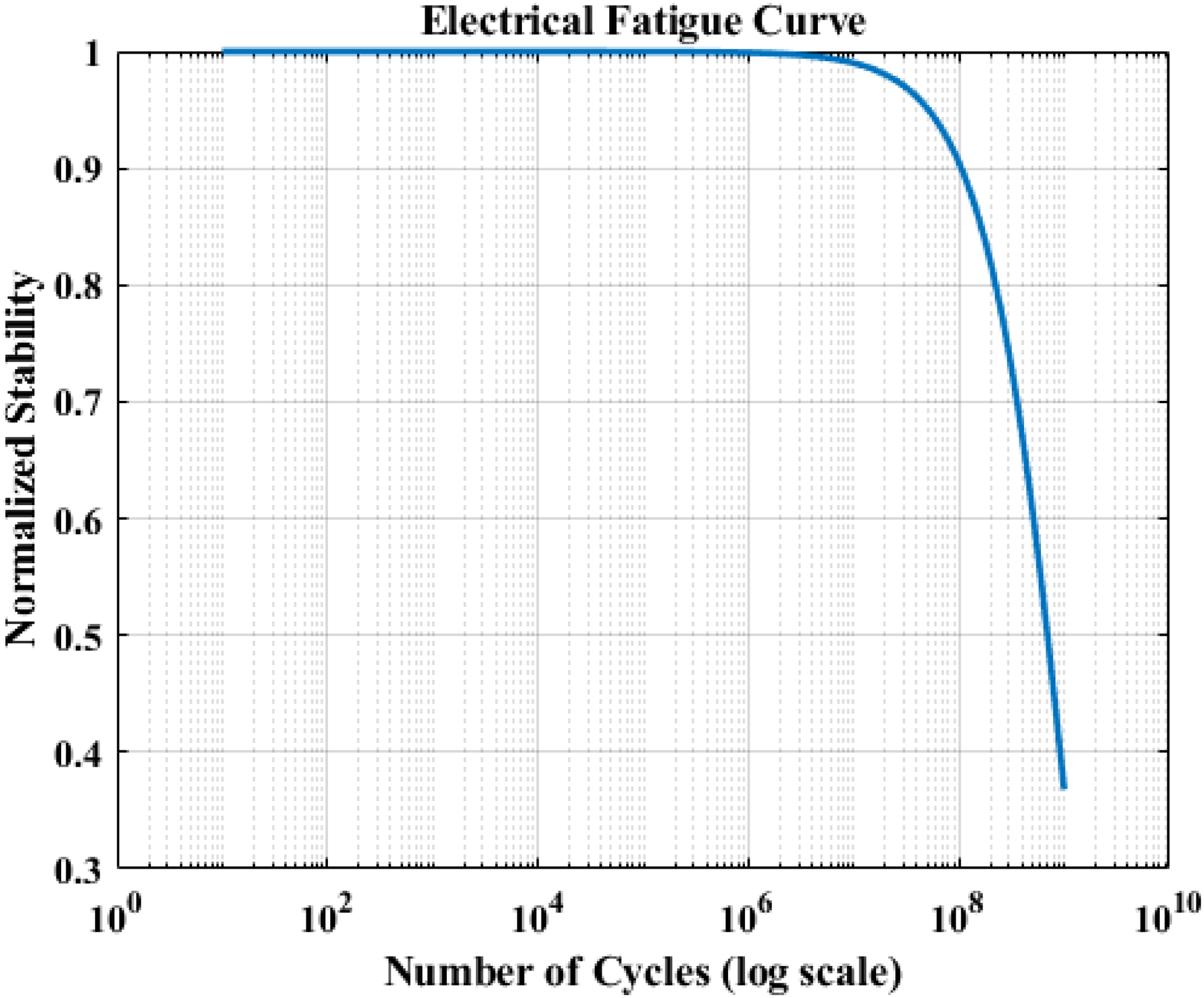
Electric fatigue.
Electrical breakdown refers to the point at which a dielectric material begins to conduct excessive current due to a high electric field, which is given in Figure 22. Here, the leakage current increases gradually with the electric field and remains very low in the beginning. Electric field around 8 V/m, there is a leakage of around 2.25 A, which is represented in a black dot is the safe operating point upto which the electric field and leakage current are stable. The red dot indicates the onset of electrical breakdown at 11 V/m, where the leakage current reaches 3 A, is where the electric field hits its limit and there is a sharp increase in the leakage current. This marks the transition toward the breakdown region highlighted in the graph. From this, it is clear that the device has high electrical breakdown tolerance, ensuring stable operation under high voltage conditions.
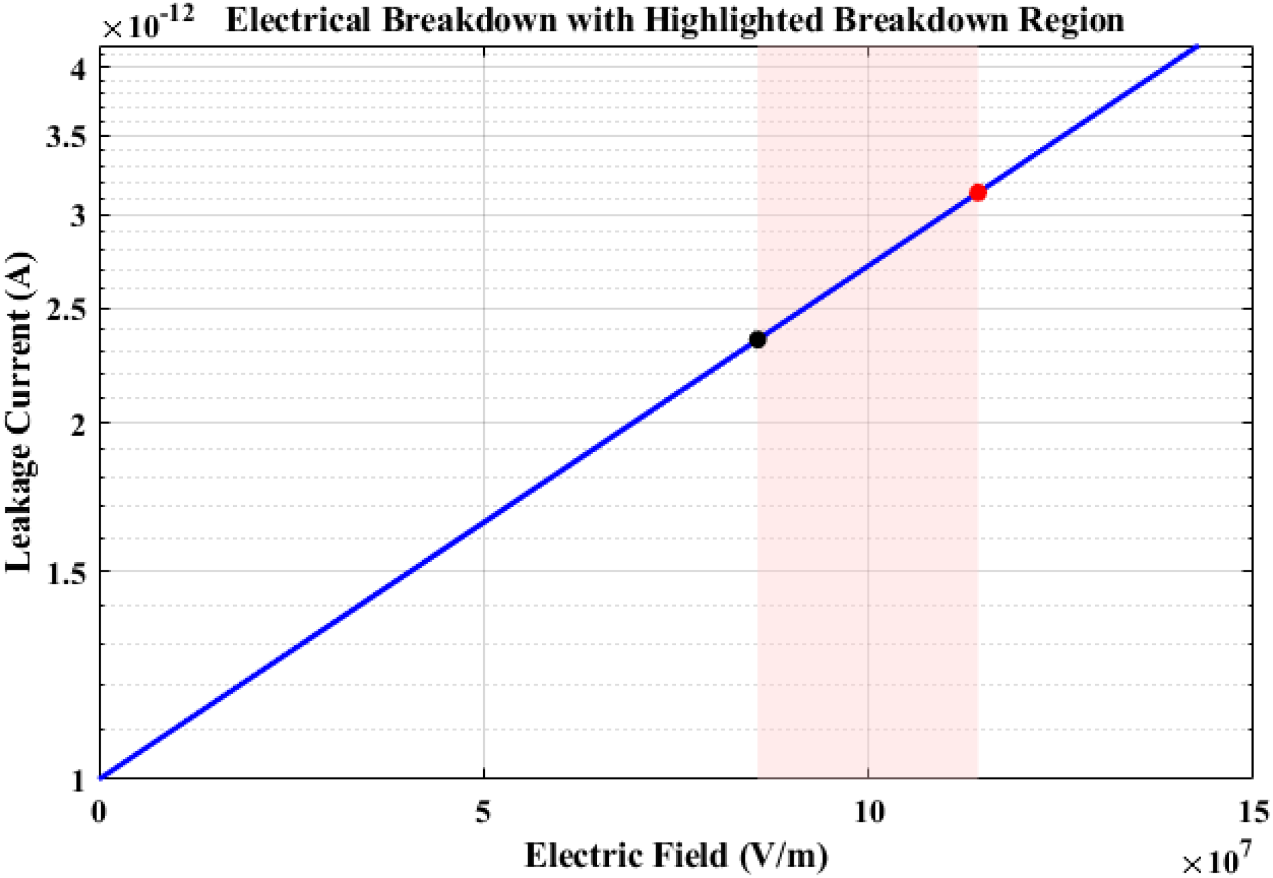
Electric breakdown.
Parameteric sensitivity analysis of the proposed design
To evaluate the robustness of the model in experimental design, a parameteric sensitivity analysis is performed in the model by making small variations in the input parameters. In real experimental small deviation occur in fabrication, so small adjutments are made in the design of the model and it is compared with the original model to determine its reliability in experimental design.
Figure 23 shows the parameteric sensitivity analysis of the proposed model based on total electrical energy, in which the red line indicates the ideal simulated proposed model and blue line indicates the proposed model with variability in parameter value. From the figure, it is noted that at times 0.05 s and 0.15 s, there is a maximum total electric energy of 3.3 × 10⁻¹⁴ J, which corresponds to the device's ability to convert mechanical energy into electrical energy. Whereas for the altered design, the total electric energy is also maximum at 0.05 s and 0.15 s with a maximum value of 2.5 × 10⁻¹⁴ J, which shows that there is a little variability between the ideal desing and altered design, which shows the reliabiliy of the model in experimental design.
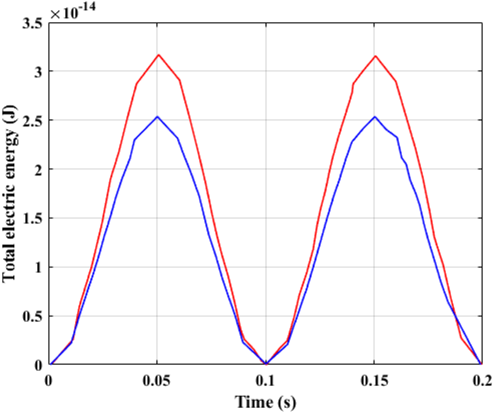
Total electrical energy.
Figure 24 shows the parameteric sensitivity analysis of the proposed model based on polarization norm, in which the red line indicates the ideal simulated proposed model and blue line indicates the proposed model with variability in parameter value. The polarization norm of the original design starts at a value close to 0 at time 0 s. It then increases rapidly, reaching a peak value of around 0.01 C/m2, at 0.05 s. Whereas, the polarization norm of the altered design starts at a value close to 0 at time 0 s. It then also increases rapidly, reaching a peak value of around 0.01 C/m2, at 0.05 s. It shows that there is almost no variability between the ideal desing and altered design, which shows the reliabiliy of the model.
Polarization norm.
Figure 25 shows the parameteric sensitivity analysis of the proposed model based on Energy Density, in which the red line indicates the ideal simulated proposed model and blue line indicates the proposed model with variability in parameter value. The energy density of the ideal design oscillates sinusoidally, reaching a peak value of 1.7 × 10⁶ J/m3 at 0.05 s and 0.15, which shows effective energy conversion at these intervals. Whereas, the energy density of the altered design also oscillates sinusoidally, reaching a peak value of 1.7 × 10⁶ J/m3 at 0.05 s and 0.15, which is very close to the ideal design and shows the reliability of the model in experimental design.
Energy density.
Figure 26 shows the parameteric sensitivity analysis of the proposed model based on Electric Potential, in which the red line indicates the ideal simulated proposed model and blue line indicates the proposed model with variability in parameter value. Between time 0.05, the potential reaches its peak value of 3.3 V, which is the maximum instantaneous electric potential reached during a single cycle, the electric potential reaches a low of −3.3 V during 0.15 s, and during this point, there is no sign of nonlinear distortion and the diaphragm is still functioning efficiently. Whereas, in the altered design, the potential reahes its peak value of 2.5 V at 0.05 s and low value of −2.5 V at 0.15 s, which is very close to the value of the original proposed desing, which indicates the reliability of experimental design of the model.
Electric potential.
Figure 27 shows the parameteric sensitivity analysis of the proposed model based on Electric Filed Norm, in which the red line indicates the ideal simulated proposed model and blue line indicates the proposed model with variability in parameter value. As noted from the figure, the proposed PMUT exhibits a rapid electrical response reaching an electric field norm maximum of 14.1 × 10⁷ V/m at 0.05 s and 0.15 s, representing a peak electromechanical action. As in times 0.1 s and 0.2 s, the electric field norm reaches zero. Whereas, the altered desing reached a maximum electric filed norm of 14.1 × 10⁷ V/m at 0.05 s and 0.15 s and 0 at 0.1 s and 0.2 s, which is similar to original design and there is almost no variations in the value, which indicates the reliability in real time performance of the model.
Electric filed norm.
Figure 28 shows the parameteric sensitivity analysis of the proposed model based on Electric Displacement Filed Norm, in which the red line indicates the ideal simulated proposed model and blue line indicates the proposed model with variability in parameter value. The proposed model has electric displacement field reaching a peak of 0.067 c/m2 at 0.05 s and 0.15 s. Whereas, the altered design has peak electric displacement field of 0.039 c/m2 at 0.05 s and 0.15 s, which is close to the original design, indicating the effectiveness of the model in real-time design.
Electric displacement field norm.
Comparative analysis of the proposed design with the existing design
In this section, a comparative overview of various designs from the literature is provided, including their shape, resonant frequencies, normalized amplitude, coupling coefficient, and piezoelectric coefficient. It allows for the assessment of different PMUT transducer performance characteristics and their suitability. The proposed PMUT design is compared with various traditional designs, which is shown in Table 3.
Comparison of the proposed design with the existing design.
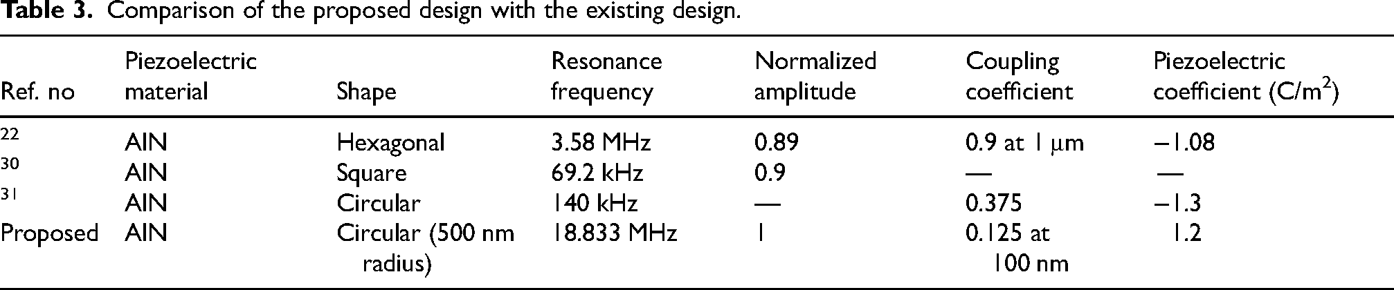
The proposed nano-scale AlN-based PMUT has a high resonance frequency of 18.833 MHz with a normalized amplitude of 1, which makes it faster and more sensitive than many existing designs. The PMUT's coupling coefficient (0.125 at 100 nm) is lower than some bulkier devices, but the ultra-miniaturized circular design of size 500 nm radius allows for better strain transfer and electromechanical efficiency required in nano-scale applications. The proposed nano-scale AlN-based PMUT is well-suited for high-frequency superficial clinical applications. It is effectively used in ophthalmic anterior-segment imaging, dermatology/skin assessments, and small-animal imaging. Its ultra-miniaturized design also supports intravascular and surface probe integration. The device's high sensitivity and biocompatibility make it ideal for wearable or implantable biomedical diagnostics.
Discussion
This section discusses about the important features in the design of PMUT in nano-scale level. In conventional techniques due to the thick diaphragm size and large dimensions of the system, there is a suboptimal electrochemical coupling reaction. It results in the diaphragm thickness dominating the mechanical stiffness, which makes the system to convert the stress improperly. While the proposed design in nano-scale level, decreases the mechanical stiffness, providing proper electrochemical reaction, resulting in the better conversion of stress in electrical energy. While designing the PMUT design in nano-scale level, the frequency of the resonance is altered, because of the high residual stress due to thin film deposition. The quality factor and amplitude are reduced by the air trapped inside the vibrating membrane and also while expanding the edges, the piezoelectric layer contracts in the center, which limits total displacement. In this design, the partial electrode structure avoids the inverse piezoelectric effect and avoids the clamping in the center. As the size of the top electrode is lesser than the lower electrode, the displacement of the model is improved. With adjusted radius of the top electrode with respect to the lower electrode, the stiffness of the model hits the target frequency of the model.
Recommended fabrication steps
The recommended fabrication steps of the proposed Nano-Scale AlN-Based Piezoelectric Micromachined Ultrasonic Transducer is explained step-by-step in this section for the clear understanding of the experimental set up of the propose model.
Step 1: silicon substrate
A Silicon crystal, which has very high resistivity is chosen to be the substrate material. The Silicon crystal is oxidised to form the Silicon Di Oxide (SiO2), which will be layered on the surface of the framework for providing electrical insulation.
Step 2: bottom electrode
A molybdenum (Mo) is to be chosen as the material for the bottom electrode formation, as it has high electrical conductivity, good SiO2 adhesion and compatibility with AlN sputtering. First, a Mo thin film of 20 nm needs to be deposited on it using the magnetron sputtering. The bottom annular electrode will be formed with an inner radius of 250 nm and an outer radius of 500 nm. The unwanted Mo can be removed through the etching process to form the partial annular electrode configuration.
Step 3: AlN piezoelectric layer
For the formation of the piezoelectric layer, a thin film of AlN with a thickness of 100 nm will be deposited using radio frequency sputtering. The AlN is to be chosen as the piezoelectric material, as it has no lead deposition, low dielectric constant and dielectric loss, and increased electrochemical coupling, which increases the efficiency of the model. The AlN piezoelectric layer can be placed in between the partial annular electrode structure.
Step 4: top electrode
Another molybdenum electrode of 20 nm will be used to form the top electrode of the partial annular electrode structure. The top electrode can be deposited by sputtering the molybdenum over the AlN piezoelectric layer. The radius of the top electrode structure is chosen to be 156.25 nm, which is around 61% of the inner radius of the bottom electrode, which helps in better electrochemical coupling. Together with the bottom electrode, the top electrode forms the partial annular electrode configuration, which concentrates the electric filed at the center of the diaphragm.
Step 5: circular diaphragm
In the formation of the circular diaphragm, anisotropic etching and lithography can be used for defining the circular diaphragm. With the help of the Deep reactive ion etching (DRIE), the silicon substrate will be etched from the backside, which creates a suspended membrane in the active region. This central circular formation reduces the mechanical stiffness of the model and enables efficient deflection.
Step 6: metallization
Thicker metal layers are to be deposited on the surface of the circular diaphragm for forming electrical interconnection with the external probing. The metal layers are made to be thicker than the electrodes for reducing the electrical resistance reliable probing of the model. Then, the top and bottom electrodes of the partial annular electrodes will be connected with larger external contact pads.
Step 7: packaging
At last, the model will be packed by forming a thin protective insulation layer on the top using SiO2 to protect the model from the external environments. Coating the model with a protective insulation layer saves the model from damage and failure due to external conditions. Proper packaging results in long-term mechanical stability of the model ensuring a better performance and reliability of the model.
Expected errors in fabrication and effects on simulation
This section discusses the possible errors in the fabrication of the proposed Nano-Scale AlN-Based Piezoelectric Micromachined Ultrasonic Transducer and their effect on the simulated results of the proposed model.
During the fabrication process, variation in the thickness of the silicon substrate or the electrode configuration, affects the stiffness and insulation of the model. In the simulation, this causes a shift in the resonance frequency and amplitude of the model. The changes in the thickness of the piezoelectric layer and circular diaphragm also has an effect on the capacitance and stiffness of the model. During the process of simulation, this changes in them affects the stiffness and resonance frequency of the model resulting in a reduced piezoelectric coefficient of the model.
Conclusion
This research aims to solve the technical challenges commonly faced by traditional micro-scale ultrasonic transducers, and proposed a nano-scale AlN-based PMUT design. By adopting a double-laminated, ultra-miniaturized circular diaphragm architecture and using partial electrode coverage
Future scope
In the future, the architecture will be integrated with monolithic integration of CMOS circuitry and flexible substrates to deploy fully conformal biomedical systems. Also, the model will be validated by using device-level experiments, which will be conducted as per the fabrication details mentioned in section 4.8 to ensure real-time application.
Footnotes
Authors’ contributions
• J. Manga: Conceptualization, methodology, writing—original draft.
• V.J.K. Kishor Sonti: Supervision, validation, writing—review and editing.
Funding
The authors received no financial support for the research, authorship, and/or publication of this article.
Data availability
No data availability for this manuscript.
Human participants and/or animals
Not applicable.
Declaration of conflicting interests
The authors declared no potential conflicts of interest with respect to the research, authorship, and/or publication of this article.