
Abstract
Additive manufacturing has become a transformative solution in telecommunications, enabling rapid and cost-effective prototyping of antennas and electronic components. This study presents the design, simulation, fabrication, and measurement of a bow-tie antenna optimized for operation in the S-band, using low-cost and easily accessible materials. Two versions of the antenna were developed, each employing a different conductive material: copper tape and low-cost conductive paint. Both designs were fabricated using a three-dimensional (3D)-printed plastic substrate, highlighting the potential for portable, field-ready antenna development. The performance of each antenna was evaluated through measurements and compared against simulated results. The analysis demonstrates that while copper tape offers reliable conductivity and consistent performance, the use of conductive paint may introduce limitations due to its lower electrical properties. These findings emphasize the importance of careful material selection in additive antenna manufacturing and offer a practical, adaptable solution for military telecommunications applications requiring fast deployment and minimal logistical overhead.
Keywords
Introduction
Military communications are crucial for applications ranging from time-critical field operations to training and logistics. The microwave spectrum (0.3–30 GHz) encompasses various telecommunications applications, including satellite communications, radar systems, and microwave transmissions. Microwaves have long been preferred due to their ability to support long-distance communication and penetrate various environmental conditions.
Currently, a significant focus in military communications is leveraging 5G network capabilities. 1 In October 2020, the US Department of Defense announced $600 million in awards for 5G experimentation and testing at five US military test sites, representing the largest full-scale 5G tests for dual-use applications in the world. 2 These initiatives aim to enhance military planning, training, and operational efficiency by integrating advanced 5G technologies.
In addition to technological advancements, key considerations for military applications include the need for customizable, low-cost solutions that enable better resource allocation and more agile responses to rapidly changing field conditions. Equally important is the deployment of resilient telecommunication systems capable of maintaining secure and reliable connectivity under adverse or unpredictable circumstances. 3
Additive manufacturing (AM), commonly known as three-dimensional (3D) printing, has revolutionized numerous scientific and technological fields, from medicine to aerospace. Especially for defense, the advantages of AM have been shown recently in various applications, such as multifunctional materials for personalized equipment with biocidal activity, showing promise in revolutionizing the Defense Industry.4–6 In antenna and radio frequency (RF) engineering, 3D printing has emerged as a versatile tool for fabricating advanced designs and structures. It has been employed to develop dielectric and metallic components of antennas. 7 AM has allowed the development of complex radiating structures at low cost, either through the metallization of the 3D-printed topologies8,9 or by employing conductive filaments, such as the very conductive Electrifi (Multi 3D LLC).10,11 In addition, metal alloys based on Gallium and Indium are used to run through 3D-printed microfluidic structures to form zig-zag and helical antenna12,13 or to add reconfigurability to standard antenna designs. 14 By enabling the fabrication of highly customized and intricate geometries, 3D printing is redefining what is achievable in antenna design, significantly enhancing their capabilities and performance. In military field applications, AM offers a valuable tool for developing a wide variety of customized structures, including antennas for various applications and frequency ranges. For instance, the US Naval Research Laboratory has created and tested 3D-printed antennas to advance radar technology, enabling new applications for the Navy. 15
Beyond individual components, AM is increasingly recognized as a critical enabler of operational responsiveness and logistical resilience during military and humanitarian missions. Recent studies have shown that AM can significantly reduce lead times, inventory requirements, material waste, and energy consumption for mission-critical spare parts, particularly those that are highly specialized, slow-moving, and difficult to forecast. 16 By shifting from physical inventory to digital design files, armed forces can improve system readiness and sustainability while operating in austere or remote environments. 16 In this context, the ability to fabricate RF and antenna components on demand aligns closely with emerging mission-based supply chain concepts, where adaptability and rapid response are prioritized over centralized production.
This paper explores the feasibility of developing low-cost, lightweight, customized antennas for military applications using AM and alternative materials. Specifically, we examine how the infill density of 3D-printed substrates affects antenna bandwidth and radiation characteristics. This capability offered by AM has already been proposed using plastic materials such as acrylonitrile butadiene styrene (ABS), 17 while a lot of effort has focused on connecting dielectric properties to infill densities and patterns of 3D printing.18–20 To this end, we designed a planar bow-tie antenna operating in the S-band frequency range. The IEEE S-band encompasses various telecommunication applications, including indoor communications (such as Bluetooth and Wi-Fi), air traffic surveillance, ship radar, and specific satellite communications.
The antenna was fabricated using 3D-printing techniques for the substrate, employing materials like High Impact Polystyrene (HIPS) due to its low dielectric losses. For the conductive elements, we utilized copper tape and low-cost conductive paint. However, our findings indicate that the low-cost conductive paint proved impractical for antenna applications, as its limited conductivity led to suboptimal performance. Conversely, the use of copper tape demonstrated the practicality of rapidly producing antennas in the field, which can be mounted on military equipment such as drones and radar systems or serve as replacements for damaged units. This approach offers a flexible and efficient solution for meeting the dynamic communication needs of military operations.
Materials and methods
Antenna design and modeling
The development of low-cost antennas based on AM was tested on a bow-tie antenna based on the design presented in Mirzaee et al. 21 For the antenna substrate, the properties of HIPS polymer were considered. HIPS material exhibits dielectric permittivity εr = 2.4 and loss tangent tanδ = 0.0014 according to measurements performed with a 1.1-GHz split-post dielectric resonator in Stevens et al. 22 The antenna setup is shown in Figure 1: the dark gray section of the schematic represents the 3D-printed plastic parts of the antenna, while the lighter orange section represents the antenna’s metallic parts. The antenna dimensions are listed in Table 1.
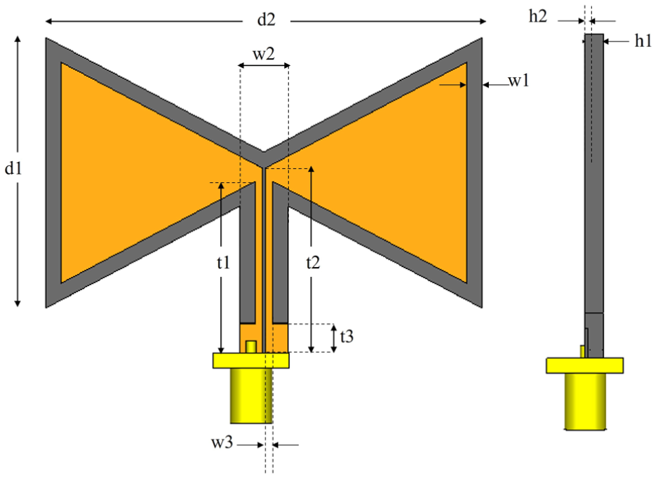
Schematic design of the bow-tie antenna with a 3D-printed substrate. The gray (dark) area is the plastic substrate, and the yellow (lighter) area is the metallic parts of the antenna.
The list of the antenna geometrical parameters.
The design includes an extruded perimeter of 2.0 mm wide (w1) and 0.5 mm deep (h2) that was also present in Mirzaee et al.’s 21 design. The target of this feature as part of the substrate is to accurately define the limits of the metallic parts during development.
Metallic parts as copper
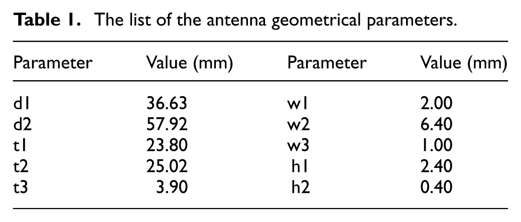
Initially, the metallic parts of the antenna were modeled as copper of 70 μm thickness that resembles the behavior of a commercially available copper tape foil. The antenna was modeled and simulated in the 0.5–6.0 GHz frequency range using CST Studio Suite®. A parametric analysis was conducted on the substrate’s dielectric permittivity (εr), which varies based on the 3D-printing pattern and infill percentage—the ratio of material to air within the printed structure. By adjusting the infill density, εr can range from approximately 1 (air) to 2.4 (solid material). This variability allows for fine-tuning the antenna’s electromagnetic properties to achieve desired performance characteristics. As the losses of HIPS are already very limited, the loss tangent (tanδ) was assumed to remain constant during the parametric analysis. The results for the antenna’s reflection coefficient (S11) are shown in Figure 2. As expected, the antenna resonance depends on the substrate material: increasing the effective permittivity of the substrate shifts the resonance frequency to lower bands.
Simulation results for the reflection coefficient (S11) of the copper-based bow-tie antenna. The dielectric permittivity of the substrate (εr) was parametrically set from 1 (air) to 2.4 (solid material) to reflect the ratio of the material infill of the 3D-printed substrate.
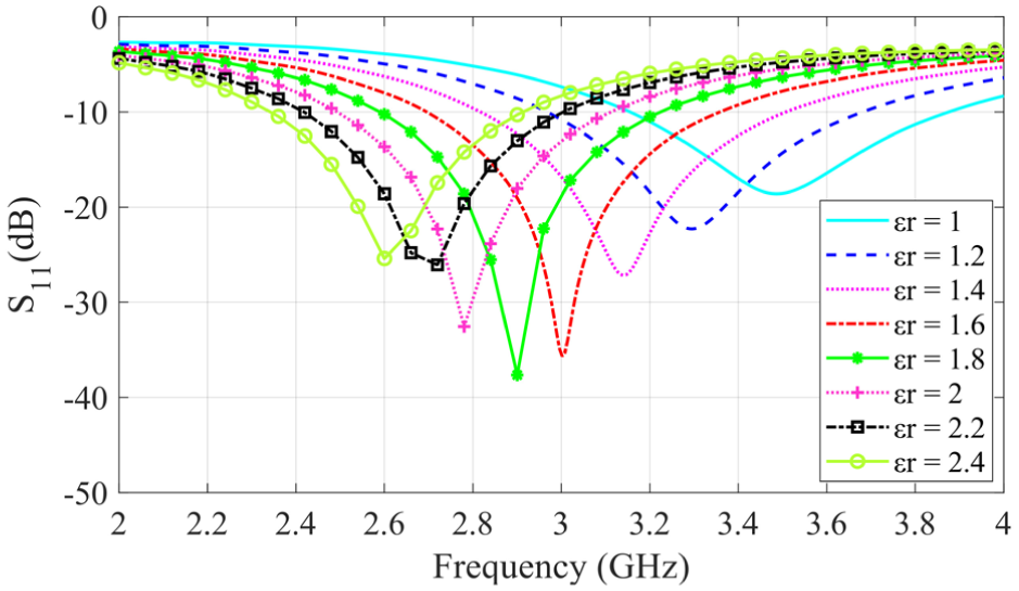
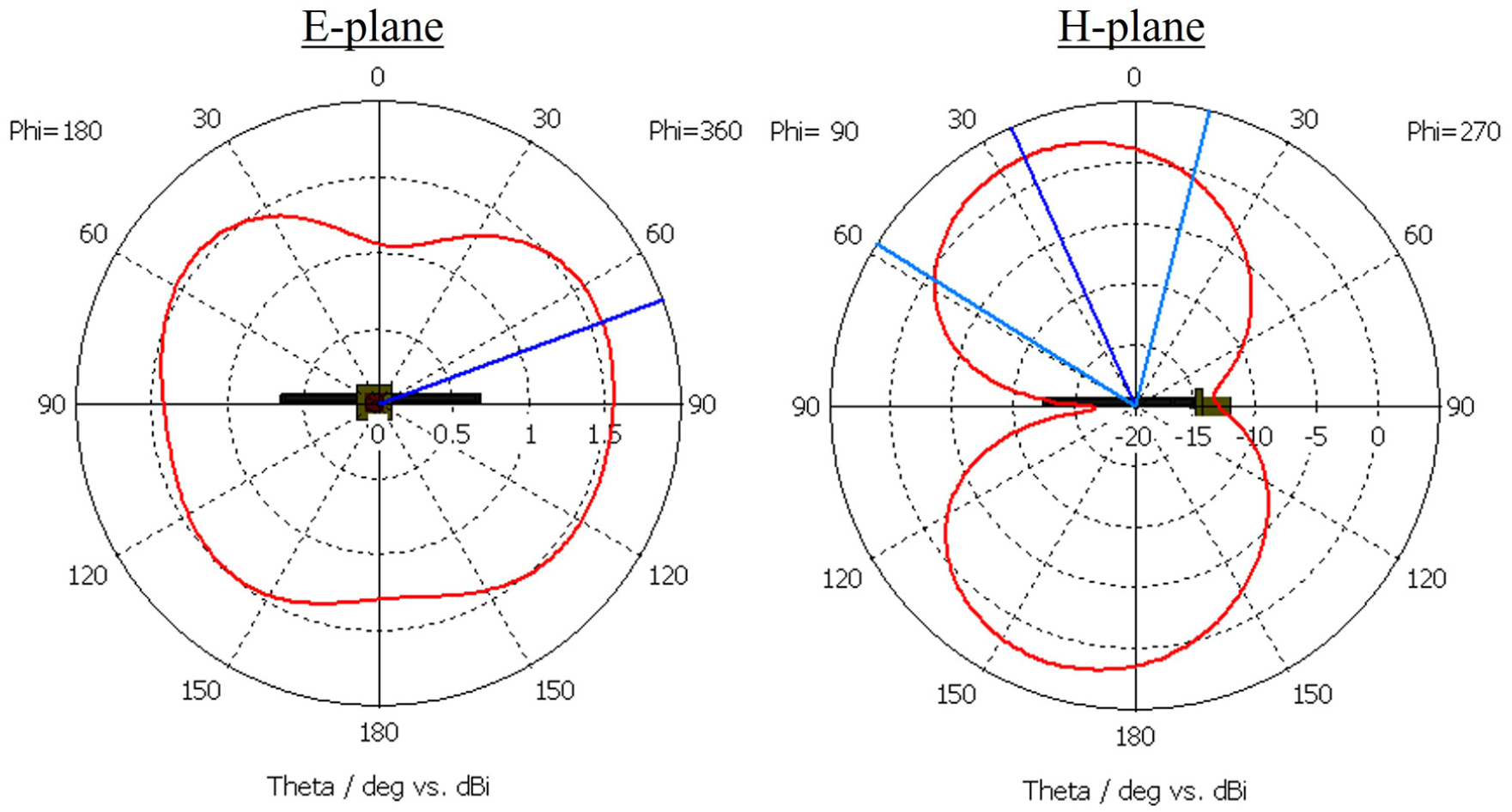
The radiation pattern of the antenna exhibits the characteristic toroidal shape typical of bow-tie antennas. Utilizing an effective dielectric permittivity (εr) of 2.2, achieved with a relatively thick substrate, results in the radiation pattern shown in Figure 3 and a gain of 2.3 dBi. An analysis of the realized gain at the resonance frequency for all materials used in the parametric study indicates that it remains consistent, ranging between 2.2 and 2.4 dBi.
Simulation results for the radiation pattern of the bow-tie antenna on a 3D-printed HIPS substrate with εr = 2.2 at 2.8 GHz.
Metallic parts as low-cost conductive paint
An alternative low-cost material examined for the metallic parts is conductive paint. Given the price variations based on conductivity levels and the volume required to cover the antenna’s metallic areas, an economical choice was made, such as Electric Paint by Bare Conductive®. According to Electric Paint’s specifications, its sheet resistance is approximately 55 Ω/sq for a 50-μm thick layer at DC. For modeling the metallic components in CST Studio Suite®, we used surfaces with sheet resistance Rs = 55 Ω/sq.
The simulation results for the reflection coefficient (S11) are shown in Figure 4, covering a frequency range from 1 GHz to 20 GHz. A parametric analysis of the substrate’s effective dielectric permittivity was also conducted for this antenna, revealing that lower infill printing densities result in a shift of the resonance frequency to higher frequencies. The limited conductivity of the chosen metal has shifted the resonance to higher frequencies, as the increased resistance restricts current flow, effectively shortening the antenna’s length. This is further evidenced by the antenna’s radiation efficiency at 2.8 GHz, measured at 3%, reaching up to 10% at 10 GHz. In addition, the reflection coefficient seems falsely improved, as ohmic losses result in less energy being reflected due to impedance mismatches at the feed. The performance degradation is also evident in the radiation pattern: instead of the expected toroidal shape around the bow-tie, only the transmission line radiates due to significant losses. This is illustrated in Figure 5, which shows the radiation pattern at 2.8 GHz.
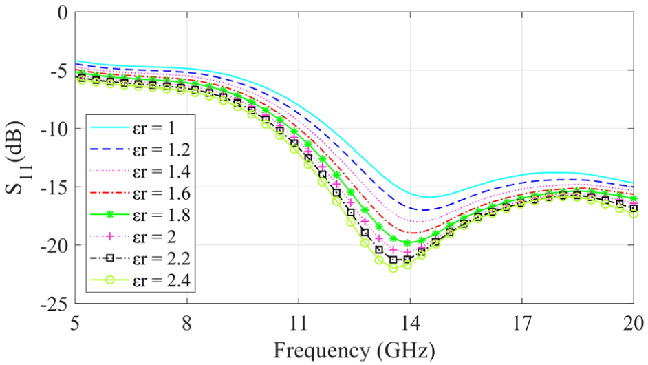
Simulation results for the reflection coefficient (S11) of the bow-tie antenna on a 3D-printed HIPS substrate with εr = 2.2 and conductive paint with Rs = 55 Ω/sq.
Simulation results for the radiation pattern of the bow-tie antenna on a 3D-printed HIPS substrate with εr = 2.2 and conductive paint with Rs = 55 Ω/sq at 2.8 GHz that show that the antenna is not operating as a bow-tie dipole because of the significant losses.
Antenna development and 3D printing
The antenna substrate was fabricated using a Creality CR200B (Shenzhen, China) 3D printer. HIPS material was utilized with a rectilinear infill pattern at 100% density. This pattern involves printing straight lines in one direction on one layer and then alternating the direction by 90 degrees on the subsequent layer, providing a balance between strength and printing speed. 23
For the copper-based bow-tie antenna, 3M™ Copper Foil Tape with a thickness of 2.6 mils (0.066 mm) was applied to cover areas within the 2.0-mm wide (w1) margins. Silicone thermal adhesive was used to attach the SMA (SubMiniature version A) connector securely.
For the conductive paint-based antenna, as already mentioned in the previous section, Electric Paint by Bare Conductive® was used. It is a non-toxic, water-based, electrically conductive paint that offers a practical solution for creating or repairing circuits on various surfaces. Given its cost-effectiveness and ease of application, Electric Paint was selected to cover the metallic areas of the antenna. It’s important to note that while Electric Paint is suitable for electronic and low-frequency applications, its conductivity is lower than that of traditional metallic materials, which will affect the antenna’s performance. This effect has been demonstrated in simulations utilizing its specified sheet resistance. For this prototype, the conductive paint was also used to attach the SMA connector. The copper-based and the conductive paint-based antennas are shown in Figure 6.
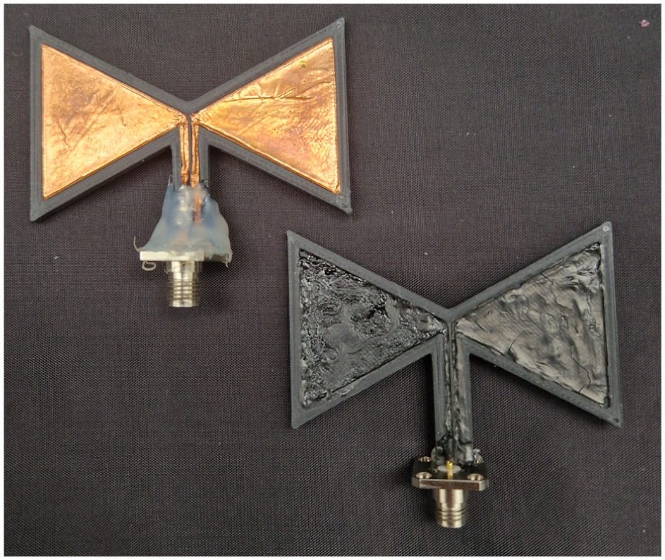
The developed 3D-printed bow-tie antennas where the metallic parts were built using copper tape (left) and low-cost conductive paint (right).
Experimental results
The reflection coefficient (S11) of the copper-based bow-tie antenna was measured in the 0.5–6.5 GHz range using a VNA (N9912C Fieldfox RF Analyzer, Keysight) (Figure 7, left). The respective bow-tie antenna with the conductive paint for its metallic parts was measured in the 1–15 GHz range using the HP 8510C VNA (Figure 7, right).
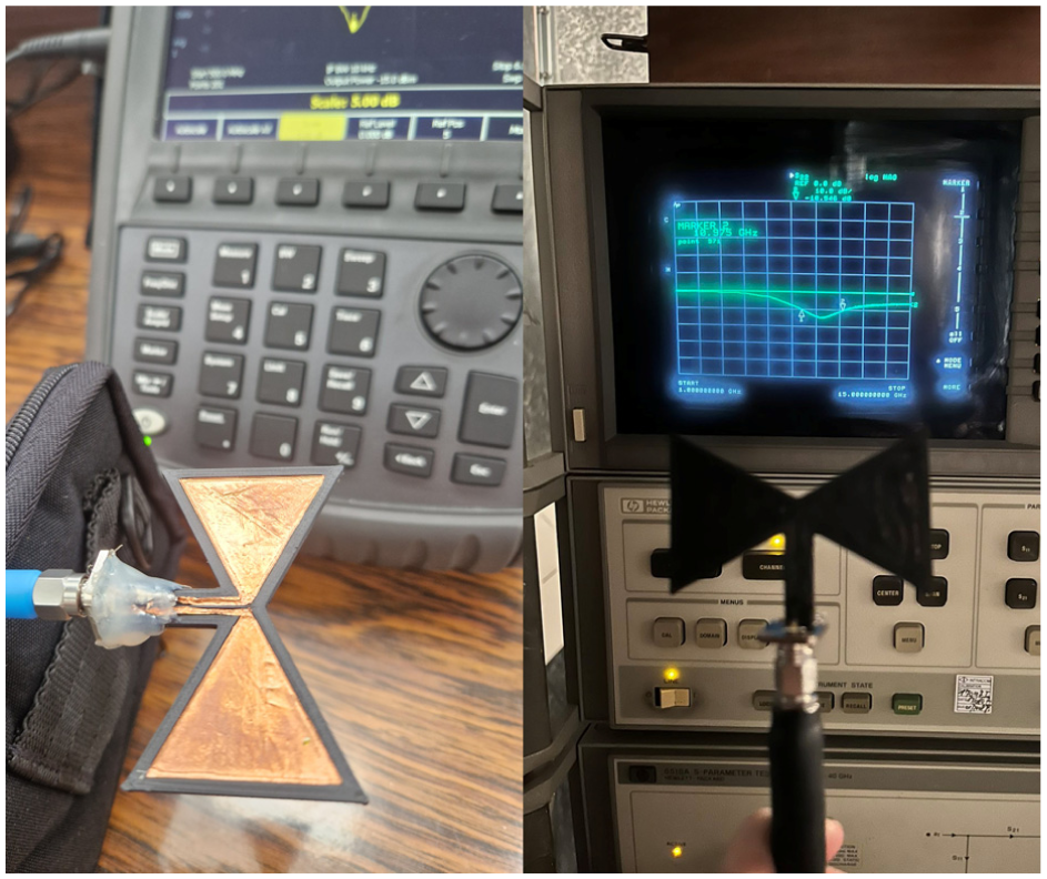
Experimental measurements of the copper-based bow-tie antenna with the N9912C Fieldfox RF analyzer by Keysight (left) and of the conductive paint-based one with the 8510C by HP (right).
The experimental results for the copper-based antenna are shown in Figure 8, alongside simulation results over the same frequency range. The simulations presented on this plot were the ones conducted assuming a substrate with an effective dielectric permittivity (εr) of 2.2, corresponding to the initially estimated infill density used during 3D printing. However, the experimental results align more closely with simulations assuming εr = 1.6. This discrepancy suggests that our initial estimation was misleading, indicating a higher air content in the substrate than originally anticipated. This highlights the critical importance of accurately estimating the substrate’s effective dielectric permittivity during the antenna design process, as miscalculations can lead to unintended frequency shifts. Despite the observed shift to a higher frequency band, the antenna demonstrates satisfactory performance within the 2.8–3.4 GHz range.
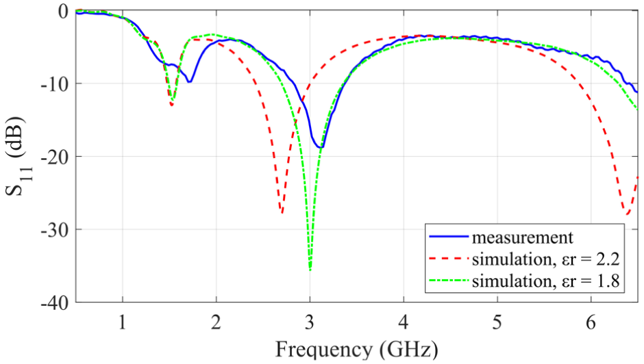
Experimental results for the reflection coefficient (S11) of the copper-based bow-tie antenna (solid line). The respective simulation results are presented using dielectric permittivity for the substrate εr = 2.2 (dashed line) and εr = 1.6 (dash-dot line).
Figure 9 presents the experimental results for the reflection coefficient (S11) of the paint-based antenna, along with simulation data for substrates with effective dielectric permittivity (εr) of 2.2 and 1.6. The observed shift to lower frequencies in the experimental results may stem from several factors, including variations in the thickness and uniformity of the applied conductive paint, which can lead to inconsistencies in conductivity and alter the antenna’s resonant frequency. In addition, post-application drying revealed surface cracks in the conductive paint, disrupting current flow and affecting performance. It’s important to note that this antenna was tested primarily for validation purposes; due to the aforementioned issues, its performance is suboptimal, rendering it impractical for real-world applications.
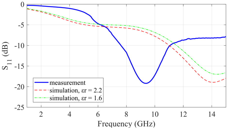
Experimental results for the reflection coefficient (S11) of the conductive paint-based bow-tie antenna (solid line). The respective simulation results are presented using dielectric permittivity for the substrate εr = 2.2 (dashed line) and εr = 1.6 (dash-dot line).
Discussion
The development of low-cost, lightweight, and application-specific antennas using readily available materials and AM techniques represents a significant advancement, particularly for field applications requiring rapid replacement or deployment of components. Among these, 3D-printed antennas show strong potential for integration into military-grade systems, enabling seamless data exchange between soldiers, vehicles, and command centers. This capability contributes directly to enhanced situational awareness, coordination, and mission adaptability.
A key enabler of this capability is the use of electromagnetic modeling and full-wave simulation tools, which allow antenna geometries and material parameters to be optimized prior to fabrication. Historically, antenna production relied on standardized substrates, limiting customization and slowing deployment. Advances in simulation accuracy, computational efficiency, and material modeling now permit reliable prediction of antenna behavior even when low-cost and nontraditional materials are used, significantly reducing design iterations and fabrication time.
One of the most promising aspects of AM is the ability to embed multiple functionalities into a single, compact antenna structure. This includes capabilities such as communication, GPS, radar, and jamming, which are highly relevant in dynamic battlefield environments. The compact design and functional versatility offered by 3D printing can reduce system complexity while increasing flexibility and field-readiness.
This study has demonstrated the feasibility of producing an S-band antenna utilizing a portable, low-cost 3D printer, HIPS as the dielectric substrate, and copper foil as the conductive layer. By adjusting the antenna’s dimensions and the substrate’s infill density, the resonance frequency can be precisely tuned to the desired range. This tunability highlights the growing role of modeling and simulation as part of a digital manufacturing workflow, where antenna designs can be rapidly modified and validated virtually to meet mission-specific requirements prior to on-demand fabrication.
However, material selection is crucial; our findings indicate that while copper foil provides satisfactory performance, low-cost conductive paints, despite their accessibility, may not offer adequate conductivity for effective antenna operation. Therefore, careful consideration of material properties is essential to ensure the antenna’s functionality and reliability in practical applications.
Conclusion
This work shows the viability of developing functional S-band antennas using AM techniques and commercially available materials. The main purpose was to examine the feasibility of low-cost and customized deployment of 3D electronic and RF components in the field. By combining simulation-guided design with AM, this approach supports a shift from centralized production to digitally distributed antenna fabrication, where design files rather than physical components can be deployed to operational environments. AM has already been proposed for the development of lightweight wearable sensors for remote biomedical monitoring of soldiers. 24 Another advantage of this approach is the potential for seamless integration of antennas with other 3D-printed components, such as customized unmanned aerial vehicles (UAVs) that have a significant role in military applications.25,26 From an operational perspective, this technology has the potential to reduce logistical dependence, enable rapid repair or replacement of damaged RF components, and improve adaptability to changing spectrum or mission requirements.
The results suggest that 3D-printed antennas can provide practical, customizable solutions for applications requiring low cost, portability, and rapid deployment—especially in military and tactical settings. Looking forward, continued improvements in simulation accuracy, printable material characterization, and conductive manufacturing techniques are expected to further close the performance gap between additively manufactured and traditionally fabricated antennas, enabling broader adoption in operational systems. In parallel, the growing availability of computational resources on portable platforms and in cloud-based environments is enabling increasingly comprehensive full-system electromagnetic simulations, allowing antenna performance to be evaluated within realistic operational setups prior to fabrication and deployment.
An important aspect to consider for these designs is the appropriate selection of materials, as electrical and mechanical properties significantly influence antenna performance. Future work should focus on enhancing the electrical characteristics of alternative conductive materials and improving overall performance, especially under real-world field conditions.
Footnotes
Funding
The authors received no financial support for the research, authorship, and/or publication of this article.
Declaration of conflicting interests
The authors declared no potential conflicts of interest with respect to the research, authorship, and/or publication of this article.