
Abstract
Abstract
The recent success of additive manufacturing processes (also called, 3D printing) in the manufacturing sector has led to a shift in the focus from simple prototyping to real production-grade technology. The enhanced capabilities of 3D printing processes to build intricate geometric shapes with high precision and resolution have led to their increased use in fabrication of microelectromechanical systems (MEMS). The 3D printing technology has offered tremendous flexibility to users for fabricating custom-built components. Over the past few decades, different types of 3D printing technologies have been developed. This article provides a comprehensive review of the recent developments and significant achievements in most widely used 3D printing technologies for MEMS fabrication, their working methodology, advantages, limitations, and potential applications. Furthermore, some of the emerging hybrid 3D printing technologies are discussed, and the current challenges associated with the 3D printing processes are addressed. Finally, future directions for process improvements in 3D printing techniques are presented.
Introduction
Additive manufacturing (AM) is a revolutionary manufacturing technology that has enabled easy fabrication of miniaturized components that are used for building microelectromechanical systems. Such systems have varied applications in fields such as aerospace, automotive, biomedical devices, electronics, and instrumentation.1–5 This technology is used to build components directly from a computer-assisted drawing package where complex 3D models can be drawn in a virtual space followed by its printing through a layer-by-layer deposition of the constituent materials.6, 7 Unlike the conventional manufacturing processes, like machining and drilling, AM does not require in-situ process control, cutting tools, coolants, or other supplementary resources. 8 One of the major driving factors of AM techniques is its ability to build miniaturized complex structural geometries using simple steps that are not accessible by conventional subtractive fabrication techniques. 9 In addition, AM techniques offer several other characteristics such as flexibility in geometrical designs, precise control, excellent feature size and shapes, uniform gradient distribution, and ability to print functionally graded materials. In recent years, the 3D printing technology has made substantial progress in terms of innovation leading to a paradigm shift from simple prototyping to mass production paving the path for MEMS device fabrication using such techniques.
Micro-electromechanical systems (MEMS) is a technology consisting of miniaturized mechanical and electromechanical elements (typically range approximately from 1 to 100 μm in size), that involve the conversion of a measured mechanical signal into a machine readable signal which could be optical, electrical, or thermal. Since its emergence in the early 1980s, MEMS has revolutionized the micro/nano research domain. 10 Initially, MEMS was developed for various applications such as pressure and temperature sensors, gas chromatographs, accelerometers, and switches for low-frequency applications. Over the past few decades, MEMS has become an integral part of several research areas such as optics, biomedical devices, therapeutic strategies, mechanical, electrical, and aerospace studies. 10 Some of the current MEMS devices include digital light processing for projectors, micro-gyroscopes within cellphone packages, accelerometers and pressure sensors within automotives, lab-on-a-chip DNA diagnostic toolkits, gas sensors for a variety of environmental, aerospace and mobility applications, radio frequency MEMS, and optoelectronics. Generally, a typical MEMS device consists of four components, namely a micro-sized platform, sensing elements, micro-sized actuators, and microelectronics for control or data handling.
MEMS devices are fabricated using conventional technologies such as surface micromachining,11–13 bulk micromachining,14–16 Lithographie, Galvanoformung, Abformung (LIGA),17, 18 wet/dry reactive etching, ultraviolet (UV) photolithography, metal deposition schemes, chemical vapor deposition (CVD) processes, wafer bonding and packaging technologies, and electroplating. These techniques are based on additive or subtractive processes that handle precise and miniscule volumes of materials in the form of thin layers on surface of silicon wafers. 19 These traditional methods are highly precise and suitable for fabrication of planar geometries. For fabrication of MEMS devices with high aspect ratios, wet etching and deep reactive ion etching processes are used where 3D features are created on stacked silicon wafers. Albeit the precision, these processes are associated with certain drawbacks such as process complexity, requirement of specialized facilities and equipment, sophisticated work environment, high lead time, and incompatibility with some flexible materials (polymers and plastics).20, 21 The emergence of these challenges has opened a window for the MEMS community to explore alternative 3D microfabrication strategies. The past decade has seen a significant increase in the utilization of AM technologies in MEMS fabrication in devices such as supercapacitors, resistors, inductors, microchannels, electronic printed circuitry, and sensor platforms.
In light of the recent progresses made in this field, this work is focused on highlighting the major advances in 3D printing for fabrication of wide-ranging MEMS devices. Considering the previous reviews published in the field of AM for MEMS applications,9, 20–24 our focus will be some of the breakthrough functional MEMS technologies which have met commercial success through 3D printing-assisted techniques. Later, the challenges and future directions for the deployment of 3D printing process for MEMS-based applications are discussed.
Additive manufacturing fabrication technologies
The international organization for standardization (ISO) and American Society for Testing and Materials (ASTM) 52900:2015 have categorized AM technologies into seven groups based on their deposition techniques, the way the material is fused or solidified, types of feed material used, and so on. 7 In this article, the discussed AM technologies have been classified on the basis of feed material/s used such as liquid, powder, and solid. Table 1 summarizes the various features of the 3D printing techniques discussed in this article.
Liquid material production
Liquid material production techniques utilize either molten materials (liquid), radiation curable resins or polymerizable materials (e.g., photopolymers) as the primary process in-feeds. A light source is used for selective curing of these materials. This section discusses the different processes that fall under this category.
Stereolithography
Features of widely used 3D printing techniques in relation to MEMS fabrication.
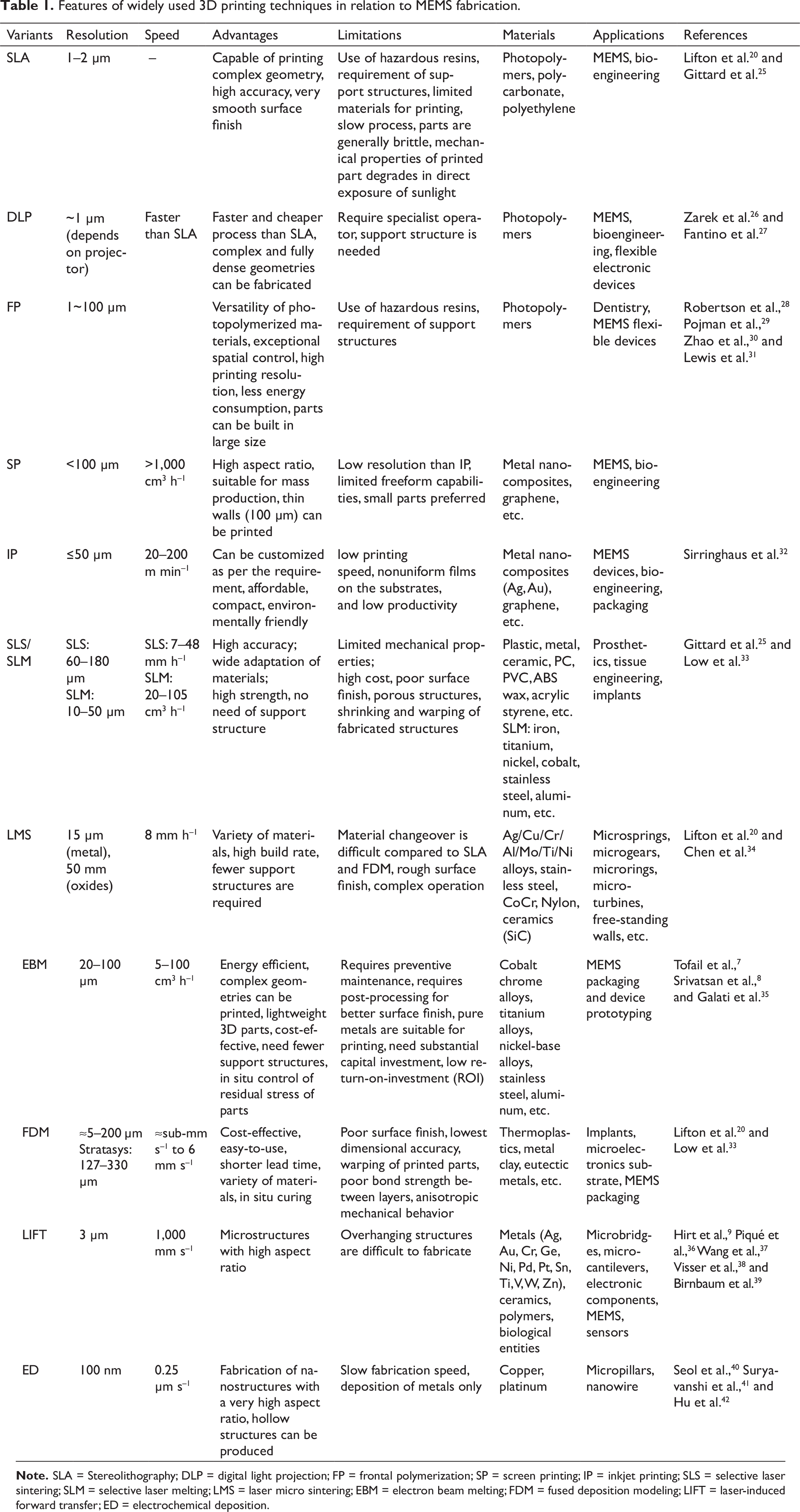
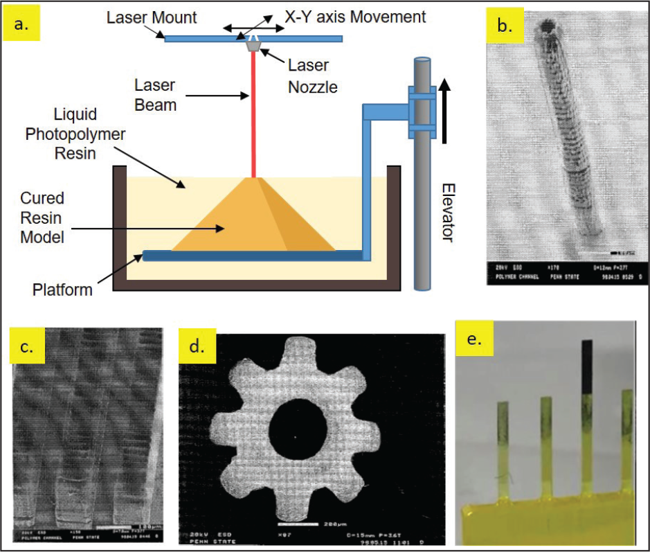
If stereolithography is utilized in the micron regime, the process is known as micro-stereolithography (µSL). 44 In a typical µSL process, an ultraviolet light is focused over a layer of photopolymers of thickness up to 1–2 μ so that submicron features can be carved in with a high degree of resolution. Zhang et al. designed an advanced microstereolithography (µSL) system which operated with a UV beam having a spot size of 5 μ. 44 Using their experimental setup, they fabricated various polymeric 3D microstructures with high aspect ratios such as microtubes (Figure 1[b]), microchannels (Figure 1[c]), microgears (Figure 1[d]), and so forth on silicon substrates. They were the first to demonstrate fabrication of 3D ceramic microgears using the µSL technique. Credi et al. successfully fabricated polymeric cantilever-based ferromagnetic microstructures by means of stereolithography. 46 Figure 1(e) shows the fabricated polymeric cantilever of 600 µm width.
Digital light projection
Digital light projection (DLP) system is an advanced variant of the microstereolithography process, in which the UV or laser light source is replaced by a simple white light source for photopolymerization. DLP uses a digital virtual photomask, a spatial light modulating (SLM) element, like a digital micromirror device (DMD) or a liquid-crystal display (LCD), to flash a single two-dimensional patterned image of each layer of a 3D model across the entire platform all at once.47, 48 The digital image is composed of many square pixels, called voxels, and the resolution of DLP can be controlled by varying the pixel size. In this process, a vat of liquid polymer is exposed to the specifically patterned light projected from a digital projector, allowing for photopolymerization of an entire two-dimensional cross section in a single exposure. The 3D solid object is fabricated by changing the vertical position of the focal plane after curing of each subsequent layer. DLP 3D printers enable fabrication of larger build sizes at faster processing speeds with relatively lower overall cost of the equipment. 1 Some other advantages of DLP 3D printing technique are rapidity, tunability of resolution, and minimum wastage of material. The DLP process requires a support structure for printing of an overhang structure or a structure that is undercut. It also requires post-curing and cleaning steps of the printed samples. Since it renders images with square voxels, the voxel effect is distinctly visible particularly for curved sections.
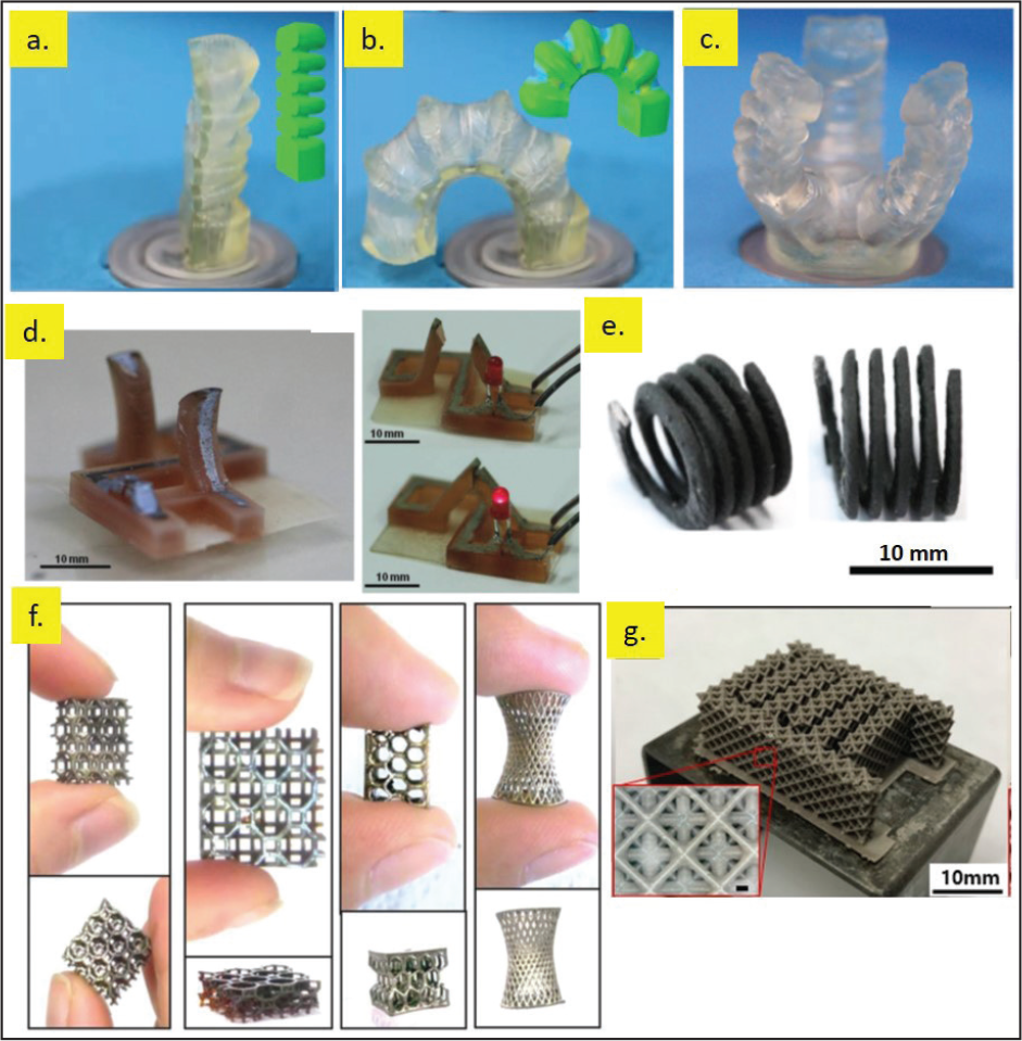
Pawar et al. reported 3D printing of a woodpile-structured hydrogel scaffolding in aqueous solution by the digital light processing technique. 49 Patel et al. utilized the DLP technique for printing of highly stretchable and UV curable (SUV) elastomers to fabricate pneumatically energized soft actuators. 50 These structures reveal excellent stretchability and hold a great potential to be used in the field of soft robotics. DLP has been used in fabrication of many complex devices for various applications such as printing of shape memory polymers for flexible electronic devices, 26 3D conductive polymeric structures,27, 51 3D electrodes, 52 and soft pneumatic micro-grippers. 53 Figures 2(a)–(g) show various DLP printed 3D structures.
Several researchers have reported another variant of microstereolithography technique, known as “mask projection stereolithography” for fabrication of MEMS devices. Mask projection stereolithography (MSLA) and DLP are similar types of 3D printing techniques, except that the MSLA uses a permanent LCD photomask. The pixel size of an LCD photomask cannot be altered, and it can only be turned ON or OFF to block the light from the LED array to guide/block into/from the photopolymer. For any optical corrections, a lens is required in this process to focus the light. However, as compared to digital projectors, the cost of an LCD photomask is much lower. Hatashi utilized a thin film transistor LCD as a dynamic mask for fabrication of optical lenses. 54 Wu et al. developed a multi-material mask projection-based stereolithography technique for fabrication of biphasic osteochondral scaffold. 55
Frontal polymerization
Over the decades, substantial development has occurred in AM technologies in terms of higher working speeds, larger build sizes and better resolution and accuracy. Frontal polymerization (FP) is a self-sustaining polymer curing process and is one of the most promising techniques in the industry today. FP is a polymerization process in which a self-propagating exothermic reaction wave transforms the liquid monomers to fully cured polymers in a localized reaction zone.28, 29 In a typical FP process, a mixture of monomer solution and the latent initiator is heated locally until the initiator is triggered for polymerization of the monomers. Once triggered, the method utilizes enthalpy or internal energy from polymerization to further drive the reaction forward and cure the material. There are three types of FP: frontal photopolymerization (FPP), isothermal frontal polymerization (IFP), and thermal frontal polymerization (TFP). These processes are discussed in detail in previously published studies. 29 In the FPP process, the polymer film is continuously cured/polymerized in a specific direction via continuous flux of radiation, usually through a UV light.56, 57 IFP process, discovered by Koike et al., 58 involves localized polymerization propagation from a high-molecular-weight solid polymer piece (methyl methacrylate) to a solution of its monomer and a thermal radical initiator. The monomer solution dissolves the polymer seeds in the presence of the thermal initiator, thus creating a localized viscous gel region which is further cured slowly. TFP involves the propagation of localized heated reaction zones resulting from the synergetic coupling of thermal transport and Arrhenius reaction rate of an exothermic polymerization process. To initiate the polymerization in the TFP process, an external small heat source, like soldering iron, is required to decompose the thermal initiators, thus converting them into free radicals. 59 The heat generated from the exothermic reaction diffuses into the adjacent regions, thereby raising the decomposition rate of thermal initiators resulting in formation of localized reaction zones. This localized thermal front further propagates through the monomer solution converting the monomers into polymers.
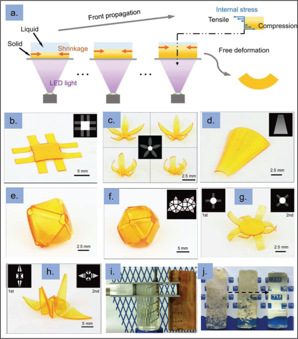
The excellent features of FP methods, such as simple fabrication protocol, shorter processing time, and high yields, make them suitable for many applications such as aerospace, automobiles, and MEMS fabrication. Zhao et al. 30 created complex three-dimensional (3D) origami structures using the FPP method with conventional photocurable polymers. The concept of their fabrication technique is based on the photopolymerization-induced volume shrinkage of liquid resin. They used an approach similar to the digital light processing (DLP) 3D printing technique. Upon irradiation by the LEDs, the layer directly exposed to the light cured at a faster rate than the adjacent layers. As the liquid–solid transition front moved through the liquid resin, the thickness of the cured polymer film increased. The temperature gradient between layers led to a non-uniform volume shrinkage resulting in formation of 3D origami structures. The volume shrinkage during photopolymerization was controlled by creating an attenuated light field using photoabsorbers. The photoabsorbers produced a light intensity gradient that controls the volume shrinkage in a sequential fashion.
Figure 3(a) shows the steps involved in formation of volume shrinkage–induced bending structures. The FP methods have provided a new and simple route to fabrication of MEMS structures for a variety of related applications such as microelectronics, biomedical microdevices, soft sensors, and actuators.
MEMS devices are also being used in biomedical applications, although they are, to some extent, limited by the biocompatibility issues. Researchers have reported various types of hydrogel-based MEMS devices such as actuators and valves.61–64 Zhao et al. presented a unique and straightforward approach for making the polydimethylsiloxane (PDMS)-based 3D origami structures by the FPP method. 30 They utilized the concept of “volume shrinkage” during the photopolymerization process. During the gradual photopolymerization, the initially cured material releases internal stress and shrinks freely, whereas newly cured material shrinks under the influence of previously cured material, resulting in the development of a nonuniform stress field in the film. Based on this concept, a variety of PDMS-based 3D origami structures was created (Figures 3[b]–[h]). Recently, Potzmann et al. 60 developed hydrogels using the UV-initiated frontal polymerization of acrylic acid in aqueous formulations. The experimental setup used for experimentation is shown in Figure 3(i). By utilizing the sulfate-sulfonyl thermal initiator, they were able to achieve first bubble-free steady-state thermal front reaction in water. Figure 3(j) shows the improvement as a result of applying the thermal initiator KBSPS and the UV initiated photoinitiation in the synthesis of a bubble-free hydrogel sample. Nuvoli et al. 65 successfully used the FP method to synthesize copolymer hydrogels of poly(N-vinylcaprolactam-co-itaconic acid). The different variants of hydrogel synthesis using FP methods have been reported in various other research works.66, 67
Screen printing
In screen printing, a liquid ink is first uniformly dispersed over the patterned screen and then squeezed with the help of an elastic squeegee through a meshed screen to print on the substrate underneath. Figure 4(a) shows the graphical illustration of the screen printing process. Using this technique, 3D structures can be created by subsequent drying of the previous layer and printing the next layer over it till the desired structure is achieved. The feature of screen printed parts can be controlled by adjusting the layer thickness. The layer thickness depends on various parameters such as thickness of mess
Screen printing and inkjet printing are suitable for roll-to-roll processing which leads to low-cost and large-scale device fabrication. Screen printing technology was used in fabrication of transistors for the first time in Bell Labs. 71 Recently, many researchers have demonstrated fabrication of transistors through screen printing at different scales. 72 Among the non-contact approaches, screen printing, in which screen mask is used to print materials onto large-area substrates with high throughput, is considered as one of the scalable 3D printing techniques and has been the most widely used technology in various domains such as flexible sensors, actuators, electrofluidic devices, 73 batteries, 74 and supercapacitors. 75 Chang et al. demonstrated the fabrication of large area flexible pressure sensors by utilizing screen printing technique. 76 Suikkola et al. fabricated stretchable interconnects by screen printing (Figure 4[c]). 69 The lines (length 188.9 mm, width 1 mm), made of silver–polymer composite ink, were screen printed on a 50-μm thick thermoplastic polyurethane (TPU) substrate (Figure 4[d]). Figures 4(e)–(g) demonstrate some of the printing capabilities of the screen printing technology. 70
Inkjet printing
Inkjet printing is a non-contact digital printing technique used for liquid phase materials. The process principally involves the controllable dispensing of ink as droplets through a micrometer-sized inkjet nozzle head with high movement resolution. The dispensed ink deposits onto a substrate in a specified pattern and multiple layers can be positioned over each other through the precision of a computer-aided design (CAD) package within the resolution limit of the printer. Three types of ink dispensing techniques, namely continuous inkjet (CIJ), electrostatic inkjet (EIJ), and drop-on-demand (DOD) printing, are used. In a typical CIJ printing system, a continuous fluid (ink) jet is produced by the pressurizing the fluid reservoir, resulting in a continuous stream of drops jetting out through a controllable micronozzle. The drop size depends on various factors such as fluid rheology, nozzle diameter, and drive frequency. Formation of unwanted drops (wastage) during the printing process limits the use of CIJ system in MEMS fabrication. This technique is mostly used for industrial applications, particularly in product marking and coding. In the EIJ printer, droplet formation occurs due to the induced electric field. At a sufficiently high applied potential, due to the electrostatic repulsion experienced at a charged liquid surface, a liquid meniscus forms known as the Taylor cone. 77 CIJ printer is capable of producing individual micro-drops with a high resolution in the controlled machining environment. In the DOD printing system, an ink drop is produced when required, making it more economical than CIJ and EIJ printing techniques.
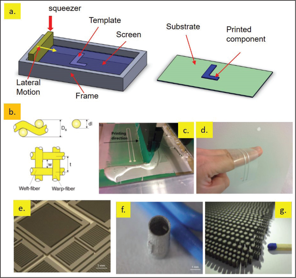
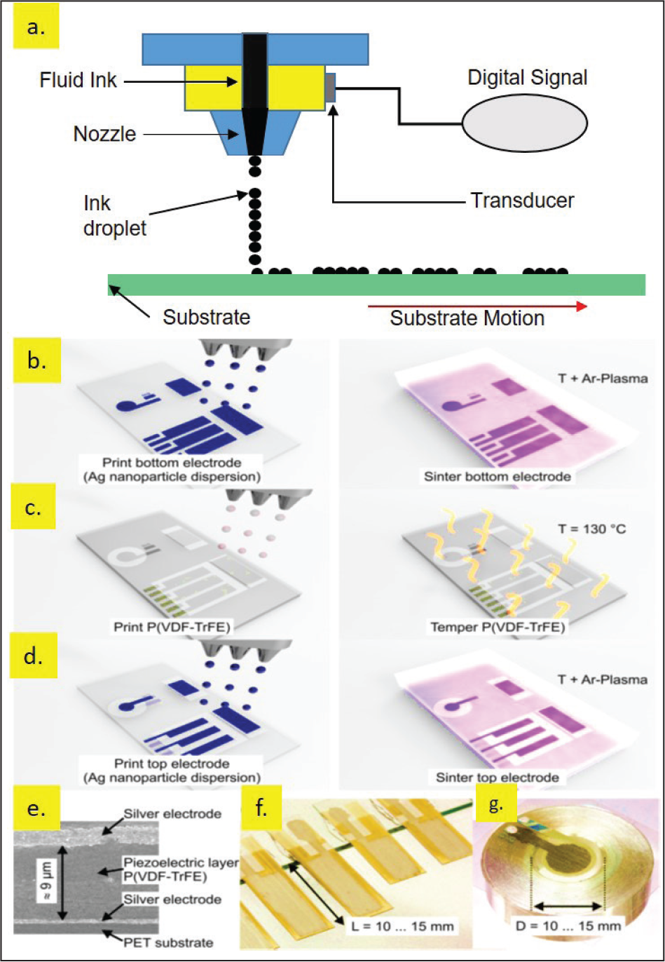
Figure 5(a) shows the schematic illustration of a typical DOD inkjet printing system. In this technology, drops are generated by actuating the printing nozzle head. The inkjet nozzle head is actuated by various mechanisms such as piezoelectric, thermal, and electro-hydrodynamic for the breaking of dispensed ink droplets.78, 79 In thermal DOD inkjet, sometimes referred to as bubble jet printing, a thin film heating element in contact with the fluid is located near the nozzle head in fluid chamber. When electric current is supplied to the heater, the fluid in direct contact gets heated, and a bubble is formed at boiling temperature. The newly formed bubble collapses rapidly due to heat transfer once the electric supply is ‘switched off’. This bubble formation and rapid collapsing produce pressure impulse which is used to eject a drop of fluid through a small orifice. The working principle of piezoelectric-driven DOD inkjet printer is similar to that of the thermal inkjet printer except the mechanism used in the pressure impulse generation. In this system, either a piezoelectric cylindrical tube (invented in 1974 by Steven Zoltan of the Clevite Corporation) 80 or a piezoelectric flat plate81, 82 is mounted to the printing head, and when voltage is applied, it contracts and squeezes the ink chamber. The sudden reduction in volume of the ink chamber generates pressure pulse, resulting in ejection of a droplet through the nozzle. 78 The ejected drop falls under the action of gravity and is influenced by the air resistance until it impinges on the substrate and spreads under the momentum acquired during its motion. Further, the surface tension aids the flow of the droplet once it reaches the surface. The drop then dries through solvent evaporation, and the leftover mark is the ink residue. Inkjet printing mainly depends on droplet separation that is directly affected by several factors such as nozzle shape and size, viscosity of ink, voltage supply of actuators, and ambient conditions of operation.
The behavior of droplet formation and liquid jetting phenomena are directly affected by the fluid properties of ink such as density (
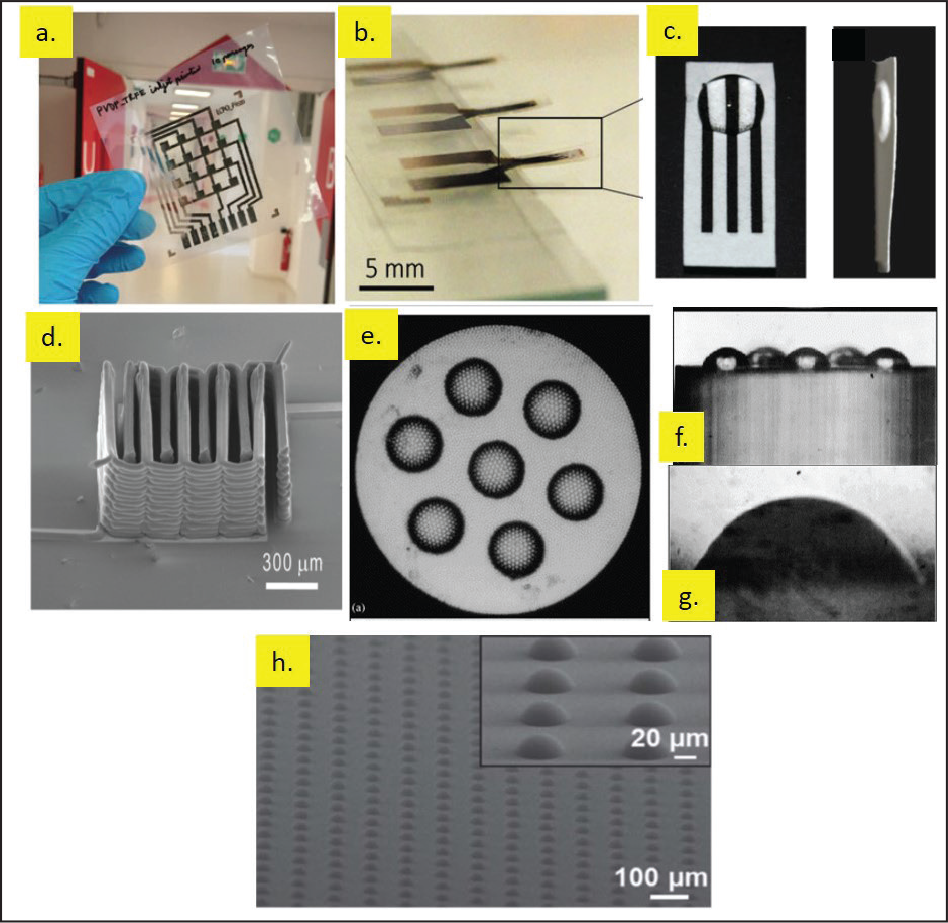
Because of their several advantages, such as excellent accuracy, good surface finish, DOD, contactless printing, ability to print the ink with lower viscosity, low wastage of ink, and low production cost, inkjet printing techniques are currently in widespread use in micromanufacturing for MEMS devices. In recent times, inkjet printing has been used for photoresist printing in the photolithography process and has also shown potential to replace the conventional spray coating/spin coating processes which are associated with several disadvantages such as non-uniform coating thicknesses, wastage of photoresists, disposability issues, hazardous waste generation, and overall high processing time.88, 89 Inkjet printing has some specific advantages over the conventional photolithography processes. For example, photolithography requires several steps such as photoresist coating, mask preparation, UV light exposure, development steps, cleaning and post baking steps, whereas in the case of inkjet printing, very few steps are required to complete the disposition of the materials like printing and annealing. Moreover, unlike the conventional photolithography process, the material can be deposited easily on to a planar/nonplanar, fragile or sensitive surface, like thin released layers, through inkjet printing, due to the extremely low inertial force exerted by a deposited drop. Further, a thick layer of the deposit can be generated by printing multiple times at the same location with high accuracy. In addition, inkjet technology has capabilities to print unconventional materials, such as magnetic materials and MEMS devices, that cannot be easily implemented using conventional fabrication processes. Inkjet printing is considered to be a key technology in the field of MEMS device fabrication. It is being widely used in printing of micro-patterns for printed circuit board (PCB), flat panel displays (FPDs), semiconductors, and sensors (biological, optical, etc.). Fuller et al. demonstrated the fabrication of MEMS by inkjet printing of Au/Ag nanoparticulate ink. 90 Using printing methodology through deposition of multiple successive layers and sintering, they were able to print an MEMS device with micro-size features and a high aspect ratio within minutes. They reported a resonant inductive coil, linear and rotary electrostatic-drive motor, and in-plane and vertical electrothermal actuator through their work. Their pioneering work opened the door for use of inkjet printing in MEMS device fabrication. Recently, inkjet printing technology has opened opportunities in fabrication of flexible electronics as well. Pabst et al. presented a lab-on-a-chip, flexible inkjet-printed polymeric actuator made by polyvinylidene fluoride trifluoroethylene (P(VDF-TrFE)). 83 Figures 5(b)–(g) show the basic steps involved in inkjet printing of actuator and fabricated cantilevers. Thuau et al. also reported the fabrication of inkjet-printed piezoelectric pressure sensors (Figure 6[a]), cantilever piezoelectric actuators (Figure 6[b]), and free-standing piezoelectric cantilever beam using the same electroactive polymers (P(VDF-TrFE)). 91 Lessing et al. used piezoelectric inkjet printing method to create high-resolution conductive electrodes on paper substrates (Figure 6[c]). 92 Sun et al. fabricated 3D interdigitated electrodes using inkjet printing methodology (Figure 6[d]). 5
In the past few years, AM techniques, such as micro-photolithography, direct ion and laser writing, LIGA, and inkjet printing, have been used in optical lens fabrication extensively. Among these technologies, inkjet printing is a preferred choice for fabrication of optical microlens due to its distinguished advantages such as contact less printing and ability to print broad range of materials on various substrates over other methods. 95 Various researchers have reported microlens fabrication through inkjet printing.96–99 Carter et al. reported uniform printing of an array of imaging sensors on the surface of an optical fiber light guide. 93 Figures 6 (e)–(g) show the inkjet-printed microdots on polished tips of optical image guides. They demonstrated the excellent reproducibility of the inkjet printing process for microlens fabrication. Kim et al. fabricated an array of multi-scale microlenses on a hydrophobic glass substrate by a simple inkjet printing technique. 94 The diameter and height of the microlens developed were 53 µm and 12 µm, respectively, as shown by the SEM images (Figure 6[h]).
Direct laser writing
Direct laser writing (DLW) is a multiphoton polymerization-based 3D printing technique that allows for fabrication of 3D structures using suitable photopolymerizable materials. In this process, a focused laser light of specified wavelength (at a frequency below the single photon threshold of photopolymers) is used to illuminate the surface of liquid photopolymerizable materials. When the pulsed laser light is tightly focused to a spot on the liquid photopolymer, it nonlinearly absorbs two or more photons resulting in localized polymerization.100–102 After successful polymerization of a small volume of material corresponding to a certain desired thickness of the polymer, the focal point of the beam is changed using a numerically controlled motor for printing the subsequent layers. By precise control of laser’s focal point size and motor movement, complex 3D features and shapes can be manufactured using DLW process. Figure 7(a) shows the basic processing steps involved in the DLW technology.
DLW possesses several advantages such as excellent fabrication compatibility with conventional planar circuits, high writing speed, high spatial resolution enabling patterning of three-dimensional micro/nanostructures with lateral feature sizes even below the diffraction limit.105, 106 Generally, DLW is capable of printing several electrically insulated materials such as hydrogels, polymers, siloxanes, and organic/inorganic hybrids. It can also be used to develop 3D molds for casting of conductive materials. However, this inversion technique is very expensive, time-consuming, and challenging for complex structures. DLW has been recognized as a favorable high-resolution lithography technique for fabrication of complex 3D polymeric structures for MEMS applications. DLW has been used in fabrication of supercapacitors, photonic crystals, and so on. Bin et al. demonstrated the fabrication of flexible micro-supercapacitors through the DLW technique. 103 They introduced the laser-induced carbonization technique for facile fabrication of flexible micro supercapacitors on flexible polyimide sheet. Figure 7(b) shows the schematic of fabrication process of capacitors with high flexibility (Figure 7[c]). Deubel et al. fabricated three-dimensional photonic-crystal templates through DLW for telecommunications applications. 100 Figure 7(d) shows the SEM micrographs of 3D photonic crystal fabricated layer by layer with 40 layers of commercially available photoresist SU-8. A massive outer wall prevents bending and reduces distortions due to polymer shrinkage during polymerization, completely fabricated by DLW. Ovsianikov et al. reported the fabrication of complex three-dimensional scaffolds made of poly(ethylene glycol) diacrylate (PEGda). The laser-assisted two-photon polymerization (2PP) was used in fabrication process. Figure 7(e) shows the SEM images of produced 3D scaffolds.
Powder material production
Powder-based 3D printing processes involve the use of materials in a powder form for printing. General examples of powder-based AM technologies include selective laser sintering (SLS), selective laser melting (SLM), laser micro sintering (LMS), and electron beam melting (EBM).
Selective laser sintering/melting
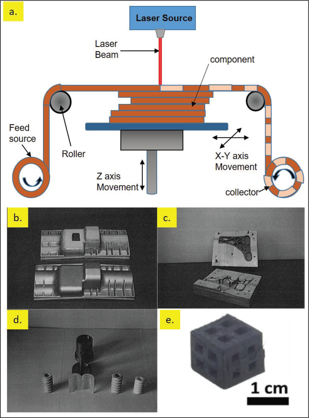
SLS is a powder-based 3D printing technique in which a part is built layer by layer by melting and sintering of powder materials, achieved through irradiation by a laser light. In a typical SLS process, the powder materials are dispersed uniformly on the bed using a roller system, and a laser beam scans a specified path over the surface, resulting in sintering of the powders in the exposed regions. The path of the laser beam follows a CAD outlay and is guided by computer numerical control. The exposed powder materials fuse together on a molecular level due to an extremely high energy density imposed by the laser beam, and the subsequent room cooling effects lead to the formation of a solid part. After a single pass of the laser beam, the powder bed is lowered down to a certain required layer thickness by the CNC system, and the powder is again dispersed over previously printed layer followed by a repetition of the irradiation step. The process is repeated until the final part is fabricated. The loose powder is removed from the bed after every irradiation and cooling transition step by using a doctor blade which again is operated through CNC. Figure 8(a) demonstrates the working principle of the SLS process.
Because of the small spot size of the laser beam, a complex structural geometry can be fabricated by this process with many intricacies. Compared to FDM, SLS does not require any support structures to build complex 3D architectures, for example, overhanging structures. The unsintered neighboring powders provide support for the overhanging parts, if any, to the subsequent layers. As SLS involves sintering and fusing of powders in fabrication of 3D solid structures, the resulting parts are produced with high porosity and low mechanical strength. A precise 3D complex microstructure can be realized through SLS by controlling several machining and process parameters such as types of laser, namely pulsed or continuous, the spot size of a laser beam, layer thickness, and controller system. The feature size of SLS printed parts also depends on material properties such as viscosity, surface tension, thermal conductivity, specific heat, powder size and shape, and melting temperature. 113 SLS is used for fabrication of polymeric samples, and metal and ceramic parts can also be created through this process.
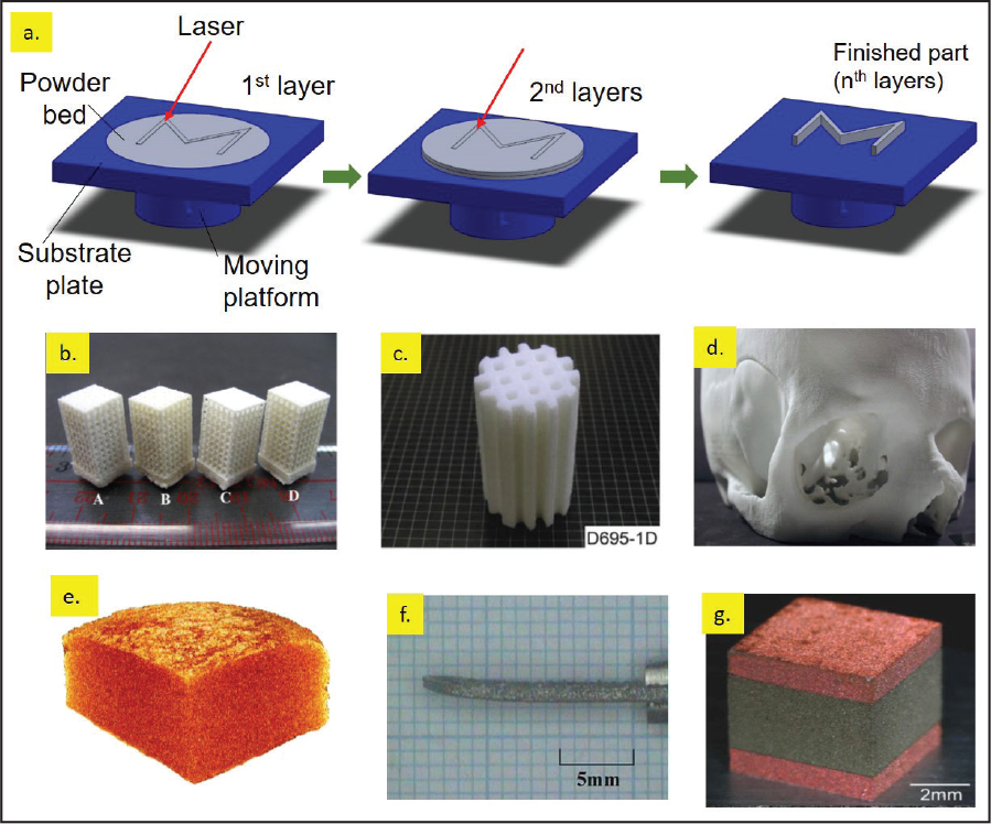
SLS has been widely used in medical industries for printing of several implants or surgical tools such as prosthetics, knee and hip implants, surgical guides and tools, surgical learning tools, and scaffolds. Duan et al. successfully fabricated 3D nanocomposite scaffolds using SLS technology. They synthesized bio-nanocomposites by combining biodegradable polymer with osteo-conductive inorganic nanospheres and used this to create a hierarchical structure (Figure 8[b]). Eshraghi et al. demonstrated the printing capabilities of nearly full-density 3D scaffolds through the SLS process (Figure 8[c]). These structures showed good mechanical strength matching with the requirements prompted through bone tissue engineering approaches. While much of the focus for 3D printing in the medical industry has been around the bone tissue engineering studies, implants, and medical equipment, one of the new areas of applications that has grown in parallel is drug development in pharmacology. With the help of 3D printing technologies like SLS, researchers have been able to now successfully 3D print customized medical pills, merge multiple pills into a single entity, and so on. Mazzoli et al. demonstrated the abilities of SLS by manufacturing a 3D human skull (Figure 8[e]). 109 SLS has been successfully employed in 3D printing of customized medical pills merging multiple pills into a single pill. Fina et al. printed oral medical drug-loaded tablets using SLS process (Figure 8[e]). 110
In the mid-1990s, a variant of SLS system, known as SLM, was developed at the Fraunhofer Institute ILT in Aachen, Germany, for printing of metallic structures. The working principles for SLS and SLM are almost similar, with the only difference being in SLM, where the powders are melted primarily due to the high energy density laser beam that is deployed in these processes. The molten materials solidify rapidly, resulting in the formation of solid structures. Also, support structures are required in SLM technology to support the overhanging metallic structures primarily due to a state change and the high fluidity during processing. The technique depends on several process parameters such as laser power, spot size, scanning speed, and layer thickness. Furthermore, an inert environment is needed in the SLM process to prevent the heated metallic structures from getting oxidized. The primary advantages of SLM over the SLS is that in the former, powders are melted and solidified, producing fully dense structures, thus making it deployable for plenty of applications such as medical and dental applications (viz. dental prostheses and cortical bone implant, etc.), 114 cooling systems, 115 light weight structures, and so on. Clare et al. used SLM technology to build a 3D cantilever beam of NiTi shape memory alloy (Figure 8[f]).
In the 2000s, another variant of SLS, called LMS, was developed by Laser Institute Mittelsachsen to produce metal microparts. 112 In LMS, a high-intensity pulsed laser beam (Q-switched Nd:YAG laser) is used for sintering of submicron-sized metallic powders. The LMS has brought down the fabrication resolution down to 10 µm range. Initially, it was developed for processing of tungsten and nickel in 3D fabrication. Recently, a variety of other materials, such as copper, ceramic, molybdenum, stainless steels, and nichrome, has been used in 3D printing of microstructures. Exner et al. printed 3D laminated microstructures of copper-molybdenum-copper using LMS (Figure 8[g]). 112 As can be seen from the figure, LMS printed microstructures are associated with poor surface finish due to inconsistent compactness of power bed and condensing effect. 112 Also, because of higher surface area-to-volume ratio, the smaller-sized metallic powders (typically, 1–2 µm) are more prone to react in the presence of humidity and oxygen resulting in corrosion of powders. Additionally, the submicron-sized powders readily self-agglomerate due to size effect. Therefore, some precautions are needed to carry out this process. However, with the increasing demand for rapid fabrication of micron-sized parts, LMS is a favorable technique for fabrication of MEMS devices.
Electron beam melting
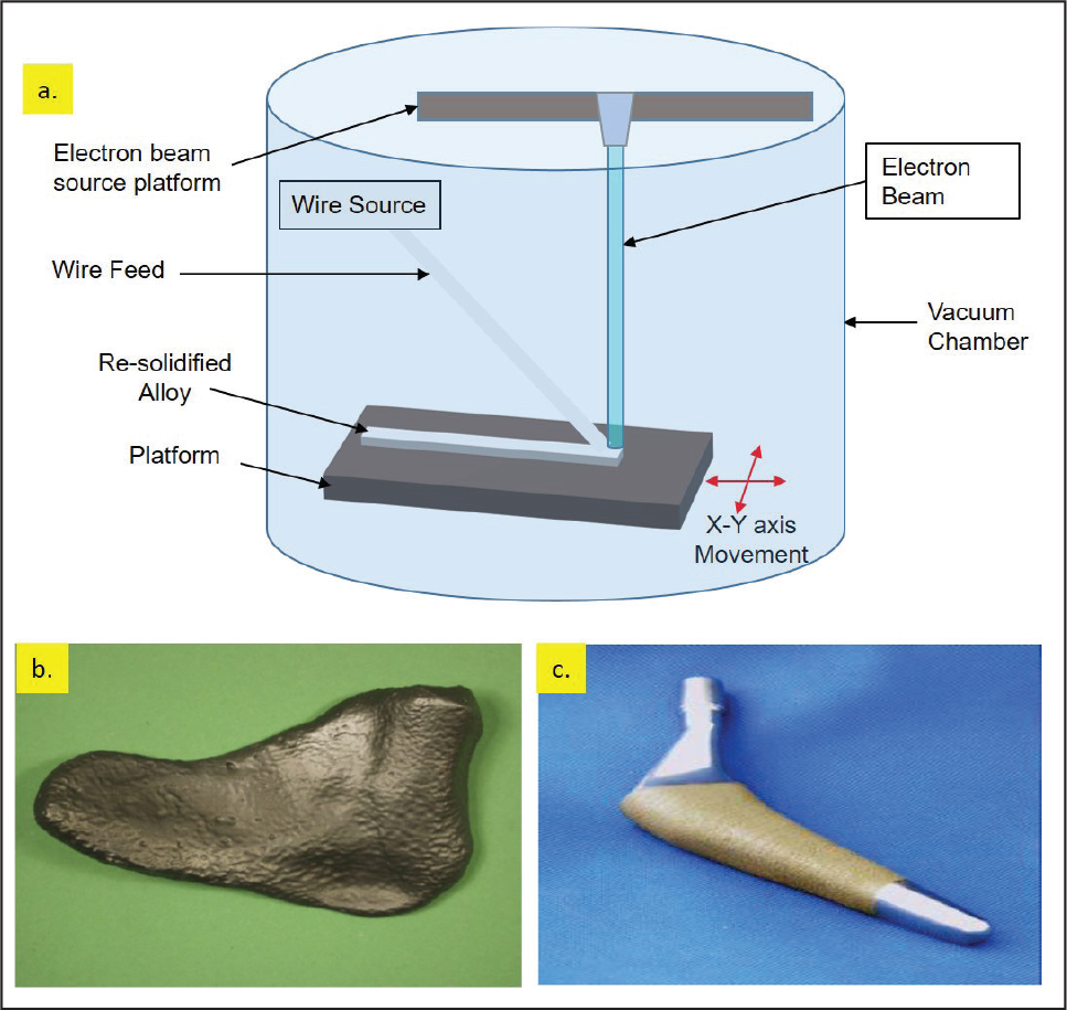
EBM is a new innovative powder bed-based AM process used for both rapid prototyping and 3D printing of metal components. In this process, an electron beam is used as the energy source for selective melting of powder materials, in a layer-by-layer fashion to fabricate elaborate 3D structures. The process requires a vacuum chamber to ensure that electrons do not collide with gas molecules, and there are no ionizations imparted so that oxidation free prints of 3D structures may result. The high energy density of electron beam results in homogeneous melting of powder materials producing printed parts through melting and solidification with high mechanical strength equivalent to injection molded parts. EBM is capable of processing materials with unprecedented strength-to-weight ratio (e.g., titanium, super alloy: Inconel 718), lowering the processing cost and reducing the substantial weight of printed samples while opening the door to a completely new paradigm. EBM offers several distinguished characteristics over the laser-based AM technologies such as reduced lead time, need for fewer support structures, energy efficient processes (uses 1/10th of energy used by laser beam), and reduced residual stresses of printed samples. Also, the high energy density of electron beam directly melts the powder, eliminating the sintering steps as used in SLS. This enables manufacturers to gain precise control over porosity of printed parts and also over mechanical strength issues. The porosity can be further tuned by adjusting the electron beam parameters. A schematic of the EBM system is shown in Figure 9(a).
Like the other powder-based 3D printing technologies, EBM-based printing has limited applications in MEMS till date. However, EBM has been used widely for printing of medical equipment, implants, skull plates (Figure 9[b]), orthopedic components such as hip, jaw, and knee replacements.109–116 Figure 9(c) shows the commercially available hip stem manufactured with EBM technology.
Gas phase deposition
Gas phase deposition (GPD) involves the deposition of thin solid films of materials to build a 3D microstructure. In GPD, material deposition occurs because of either a chemical reaction or a physical reaction. 117 The chemical reaction-based GPD technologies exploit the deposition of thin sold films directly from chemical reactions between the reactive gases and/or liquid precursor with the substrate material. The chemical reaction also results in some by-products in forms of gases, other solids, and so on. Some of the chemical reaction-based GPD technologies are: CVD, electrodeposition, epitaxy, and thermal oxidation. The physical reaction-based GPD technologies are characterized by deposition of materials in vapor phase directly on the surface of the substrate. Currently, a variety of CVD processes are available in the market, namely low pressure CVD, atmospheric pressure chemical vapor deposition (APCVD), laser chemical vapor deposition (LCVD), reactive chemical vapor deposition (RCVD), metal-organic chemical vapor deposition (MOCVD), photochemical vapor deposition (PVD), chemical vapor infiltration, plasma-assisted chemical vapor deposition (PACVD), plasma-enhanced chemical vapor deposition (PECVD), and chemical beam epitaxy. The fundamental principles of these processes are almost similar except the energy source used. The detailed description of these techniques is available in a review article by Vaezi et al. 118
Because of the versatility and capability of processing almost all kinds of materials, such as metals, alloys, and intermetallic compounds, gas phase technology has become an obvious choice for MEMS fabrication. Among the various deposition strategies, CVD, PVD, thermal oxidation, and electrodeposition are the most commonly used processes for MEMS. Kusdianto et al. used a hybrid PECVD and PVD for fabrication of TiO2-Ag nanocomposite thin films for the first time.
119
They used Ag and TiO2 nanoparticles as precursor molecules to fabricate a nanocomposite film in a single step process, which is very helpful for a photocatalytic process. Mercier et al. used RCVD process for processing of
Solid material production
Fused deposition modeling (FDM)
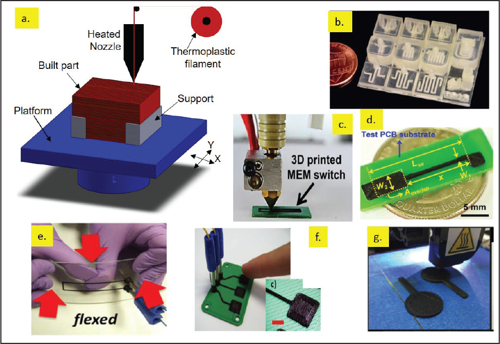
FDM-based 3D printing techniques have attracted a lot of interest in the last decade owing to their simplicity and relatively inexpensive nature. In FDM processes, the 3D structure is fabricated by depositing semi-molten materials which is extruded through a heating nozzle, over a preheated bed. The printed filament cools at room temperature and adheres to previously deposited layers to build up a solid 3D structure. The schematic diagram of a typical FDM process is shown in Figure 11(a). Starting from the printing of thermoplastics, FDM has shown its significance in many applications such as aerospace, automobiles, and electronics. Because of its low cost, simplicity, compact size, low risk, and a variety of other desirable properties, FDM technology has entered into people’s homes. People have started customizing final products according to their needs.
The quality of FDM printed samples depends on numerous factors such as printing parameters (raster angle, built orientation, printing speed, etc.), working environment (temperature, humidity), and physical parameters of materials (thermal conductivity, viscosity, surface tension) . So, the FDM printed structures are generally associated with poor resolution, poor surface finish, and low mechanical strength. The fabrication of 3D structures with submicron/nano dimensions by FDM is still a challenge and needs some improvements in the fabrication strategy. In the recent years, it has gained wide interest in the field of MEMS fabrication for developing 3D electrical components, (resistors, capacitors, and inductors, Figure 11[b]), 123 3D polymeric switches (Figures 11[c] and [d]), 124 flex sensors and capacitive buttons (Figures 11[e] and [f]), 112 three-dimensional electrodes (3DEs) (Figure 11[g]), 113 MEMS packaging, and so on. Wu et al. 123 reported a 3D “smart cap” with an embedded inductor—a wireless passive sensor, and so on. The 3D microstructures including both supporting and sacrificial structures were constructed with a resolution of 30 μm using the FDM technology equipped with a multiple nozzle system. After removing the sacrificial materials, suspended silver particles were injected subsequently and solidified as the metallic elements/interconnects. This was probably the first demonstration of a comprehensive FDM technology for printing 3D polymer with liquid metal paste filling for MEMS application.
Sheet lamination
In this type of AM process, thin layers of pre-patterned sheets of material are stacked on top of each other and bonded by either using a heat source or adhesives. If sheets are laminated using the ultrasonic bonding process, the process is referred as ultrasonic additive manufacturing (UAM), and if the adhesive is used in lamination of stacked sheets then it is called laminated object manufacturing (LOM). Figure 12(a) depicts the process scheme for LOM.
Sheet lamination techniques have several advantages such as inexpensive processing, high volumetric build rate, good robustness, high process printing capability of a combination of materials, and composites. These techniques exhibit some limitations as well such as availability of suitable binding material, requirement of thin sheets of material, and low resolution of complex parts. However, sheet lamination techniques have been utilized for fabrication of various 3D microstructures such as microsensors, microreactors, micro-fuel cell components, and heat exchangers. Also, LOM is suitable for development of rapid tooling. Mueller et al. developed several casting patterns and molds for metal casting, namely cable sleeve of wall thickness of 3 mm for aluminum casting, and LOM mold with injected wax pattern for axle bracket (Figure 12[c]). 127
Advanced additive manufacturing technologies
Several advanced AM technologies have emerged recently for fabrication of microstructures with superior characteristics. Some of these technologies are discussed in this section.
Laser-induced forward transfer
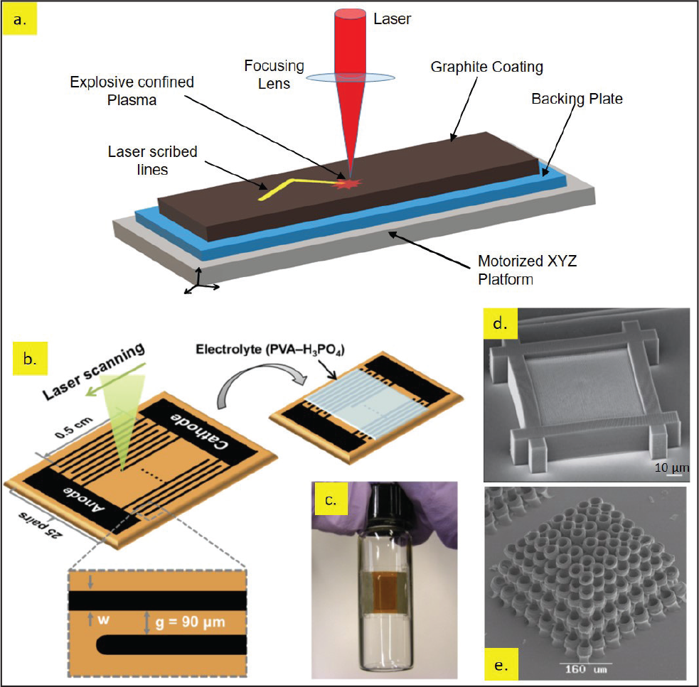
The laser induced forward transfer (LIFT) is a DLW digital 3D printing technology that is based on transfer of materials by ablation. LIFT was first demonstrated by Bohandy et al. in 1986 for two-dimensional metal patterning.
129
LIFT process involves the ejection and transfer of liquid material droplets from a thin film coated onto the rear side of a laser-transparent support substrate (carrier). Transfer is stimulated by focusing a series of pulsed laser beam on the support-film interface, where local heating and melting and/or partial vaporization of thin film provide the momentum to project the liquid material droplets to a receiving substrate placed below the support substrate. The droplets quickly cool down and solidify over the receiving substrate, and a complex 3D structure is created by subsequent layer-by-layer deposition of droplets. Figure 13(a) depicts the basic concept of the LIFT process. The support substrate is typically made of laser-transparent substrate, namely glass slide whose one side is coated with a thin solid film (
The LIFT technique is particularly fascinating due to its simplicity and versatility for micropatterning of a wide range of materials in both solid phase (metals, polymers, ceramic) and liquid phase (sol gel, viscous nanopaste, graphene ink) or even biological entities (cell cultures, deoxyribonucleic acid (DNA)). 36 LIFT, a single-step direct printing technique, operates under the ambient atmospheric conditions which makes it one of the most adaptable 3D printing technologies. In addition, LIFT process exhibits several characteristics like compatibility with flexible substrates, nondestructive and rapid, high lateral resolution of printed microstructures, and so on. However, in the LIFT process, adhesion of liquid droplets on the receiver substrate is a critical issue. So, preprocessing steps, like removal of surface oxides from the non-noble metal substrates and roughening of top surfaces of polymeric or ceramic substrates, are required to ensure proper adhesion between liquid droplet and the substrate. LIFT is best suited for printing of 3D microstructures with high aspect ratios. 9
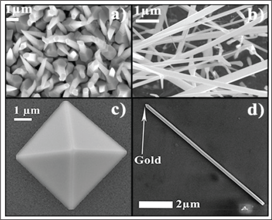
LIFT process has shown its potential to be an alternative fabrication technique for various applications such as fabrication of electronic components (organic thin film transistors, organic light emitting diode [OLED]), sensors, and MEMS.37, 131 LIFT is best suited for printing of 3D microstructures with high aspect ratio. 9 Zenou et al. demonstrated the 3D printed metal pillars with a very high aspect ratio (>20). 130 The thermally induced nozzle (TIN) assisted LIFT process allowed the pileup of droplets over each other resulting in fabrication of copper pillars. Figure 13(b) depicts an array of vertical micropillars, each composed of 400 droplets. Figure 13(c) shows SEM images of metallic bent micropillars with the bent angle of 30 degrees. These micropillars are fabricated in two steps: first, an upright pillar is printed by successive deposition of droplets, and then next 100 droplets are printed with each new droplet shifted by a distance ΔD from its previous layer. Such micropillars have gained much attention in various fields such as bioengineering, photonics, micromechanics, and micro-batteries.5, 132 Figures 13(d) and (e) depict the 3D microstructures made with metal composites. The bi-metal microstructure is composed of a copper slab and an array of gold comb printed on top of it. In the process, first copper droplets were deposited on the receiver substrate, and subsequently, gold droplets were deposited to fabricate copper slab and gold comb fingers, respectively. Therefore, the LIFT process requires fewer processing steps than conventional IC fabrication techniques.
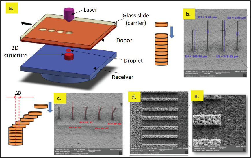
In the past decade, several variants of LIFT techniques have been developed such as dynamic release layer LIFT (DRL-LIFT), 133 matrix-assisted pulsed laser evaporation-direct write (MAPLE-DW) technique, 134 laser-induced thermal imaging (LITI), 135 long pulsed LIFT (LP-LIFT), 136 and laser molecular implantation (LMI). 137 In DRL-LIFT technique, an additional sacrificial layer, called as dynamic release layer, is placed between the carrier and donor which absorbs the incident laser pulse and vaporization fully due to localized heating. The full vaporization of DRL results in uniform pressure build up at interface and facilitates effective transfer of donor materials.
Electrochemical deposition
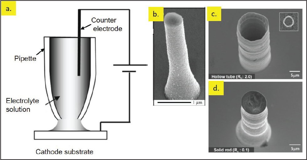
Electrochemical deposition involves deposition of thin solid films of metals onto an electrically conductive surface (electrode) in the presence of electrolyte solutions. This technique requires three electrodes, namely, working, counter, and reference electrodes submerged in an electrolyte solution. The working electrode is the object over which thin solid films will be deposited, the counter electrode is used to complete the electronic circuit and the reference electrode is used as a fixed reference point for the potentiostat. When sufficient current is passed through the solution, the metal ions are reduced at the cathode (working electrode) resulting in deposition of metallic ions over it. Figure 14(a) shows the schematic diagram of a typical ED process. As can be seen, ED setup consists of a pipette filled with metal salt solution which moves towards a working electrode (substrate). A liquid meniscus forms between the pipette and the substrate upon contact of the electrolyte. When an electric field is supplied between the electrodes, an electrochemical reduction starts in the presence of the electrolyte solution, resulting in deposition of metallic ions. By controlling the pipette movement, complex 3D geometries can be printed using this technique.
ED process is governed by the Faraday’s law of electrolysis which is as follows: (a) the amount of any material deposited due to electrolysis is directly proportional to the quantity of electricity (I) that passes through the electrolyte; (b) the amount of any material deposited by the same quantity of electricity is proportional to its chemical equivalent weight. Thus, Faraday’s law can be written as
ED technique has enabled the fabrication of 3D complex geometries of pure metals without the need of post-processing steps. This technology has been used in many applications such as fabrication of nanowires (Figure 14[b]), atomic force microscopy (AFM) probes, hollow microtubes (Figure 14[c]), and solid microrods (Figure 14[d]).40–42 This process has much potential for fabrication of MEMS in future.
Friction-based additive manufacturing
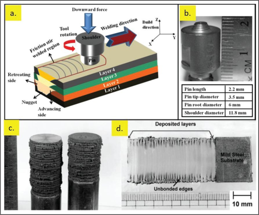
Friction-based AM is a hybrid 3D printing technology that utilizes the concept of friction welding. Friction welding is a solid-state joining process in which materials are joined due to coalescence of materials at high temperatures. The frictional heat is generated at the interface of components due to relative motion between the two workpieces under compressive loads. There are seven variants of FAT technologies such as linear friction welding (LFW), rotary friction welding (RFW), friction stir additive manufacturing (FSAM), additive friction stir welding (AFS), friction surfacing (FS), friction deposition (FD), and friction-assisted (lap) seam welding (FASW). 138 Among these, in LFW and RFW process, direct friction welding takes place, whereas in case of FD and FS methods, additional material is required during joining of two surfaces. Figure 15(a) demonstrates a schematic illustration of FSAM process, in which a non-consumable rotating tool is inserted into the overlap area where sheets need to be joined and navigated along a joint line. The tool comprises a shoulder and pin which is custom designed for specific purposes (Figure 15[b]).
Dilip et al. utilized friction deposition-based AM technique to build 3D cylindrical rods. 140 In deposition welding, a consumable rotating rod is rubbed over the substrate under continuous loading. The rubbing between the rod and substrate generates heat at the interface resulting in plastic deformation of materials and subsequent built-up formation. The rotating rod is stopped and withdrawn from the substrate after successful formation of one layer. The process is repeated till the final 3D structure is achieved. Figure 15(c) shows the formation of a cylindrical rod through a layer-by-layer deposition of materials, which can also be visualized from the micrograph of the rod (Figure 15[d]). The friction-based 3D printing requires processing post fabrication. Till now, this technology is not utilized in MEMS area, but it can be a game changer as dissimilar materials can be joined together by these processes.
Complex cellular castings
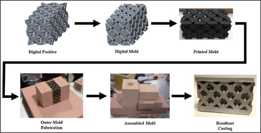
Complex cellular casting is one of the most promising techniques which is based on a hybrid AM and traditional sand casting process. In this process, AM technology is used to make 3D patterns that are then used in mold fabrication for subsequent conventional metal casting process. Pattern making steps can also be omitted by printing the mold directly with integrated gating systems. This process is referred to as pattern-less casting via indirect 3D printing. 141 Due to superior mechanical strength and lightweight characteristics of the printed parts, the cellular structure is widely utilized in aerospace and defense industries, but the fabrication of complex cellular structures is a complicated process as it needs complex mold making. The combination of AM and casting has made it possible to develop complex 3D cellular structures in an efficient manner. Snelling et al. demonstrated the fabrication of metallic cellular structures by using metal casting into 3D printed pattern-less sand molds. 142 The fabrication steps are illustrated in Figure 16. In the process, a computer-aided designed model of the mold was 3D printed, and following a cleaning step, the mold was used to cast the metals.
The complex cellular casting is a relatively new technology and has much potential in MEMS fabrication.
Outlook
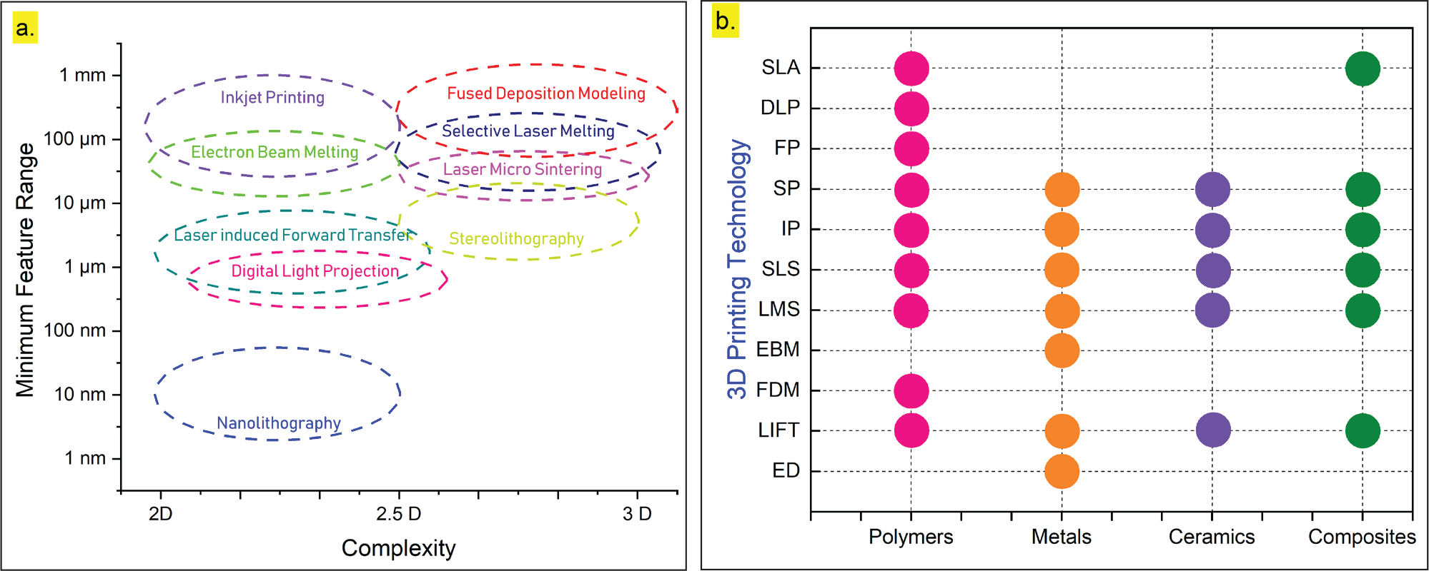
In this article, we have discussed various 3D printing technologies which are being used or can be potentially utilized in MEMS fabrication in future. Figure 17(a) depicts the minimum feature size, complexity achieved by 3D printing technology. Figure 17(b) shows the material processing capability of 3D printing. In addition, Table 1 summarizes the various features of the 3D printing techniques discussed in this article. These landscapes may help a user in appropriate AM technology selection.
AM technologies have seen a sustainable growth for MEMS fabrication and their industrial-scale implementation. It is expected that by the year 2020, most of the major manufacturing industries will switch over to AM technologies. Since the patent expiration on FDM-based 3D printing and stereolithography in 2009 and 2014, respectively, 143 a substantial progress has been made toward the development of a versatile 3D printing technology. AM can theoretically remove the inventory requirements from the industries as they are suitable for on-demand manufacturing. Customers can send a customized CAD file directly to the manufacturers and get the printed objects at their workplace or home. AM has slowly become a viable alternative to traditional MEMS fabrication.
However, considerable challenges are associated with these traditional AM processes for fabrication of MEMS. Most of the 3D printed samples possess considerable surface roughness resulting in application failure of devices, particularly in microfluidic and microelectronics applications. Since their invention, a significant advancement has been made in the field of 3D printing techniques. However, to adopt the printing capabilities of advanced materials/composites, a significant upgrade in the technology is required. In addition, 3D printing is highly dependent on material properties such as viscosity, melting temperature, thermal conductivity, and density. Therefore, an extensive study is needed for each material/composite to explore its printing feasibility. The selection of optimized process parameters for the 3D printing techniques will also be a key factor in its future growth rate. A few other challenges for the AM technologies include high initial production cost, printing time, and size of objects. Some of the AM technologies, like screen printing and inkjet printing, are capable of printing on large area substrates, but limitations are still prevalent.
Another major challenge of AM technologies is reproducibility. Since parts are fabricated layer by layer, printing parameters may vary within machines or their performance. Environmental conditions, like temperature and humidity, also influence the printing process. Powder-based AM technologies use materials in the powder form whose size and shapes are not uniform, resulting in nonuniform sintering of particles. Further, several multimaterial-based composites have attracted interest in manufacturing of devices through AM technologies, which necessitates extensive studies of interaction between these materials for better control over the printing process.
Additive manufacturing technology landscape. (a) Comparison of minimum feature size and complexity of produced geometries. (b) Material processing capabilities.
Summary
The fabrication capabilities of 3D printing technologies on the micro/nano length scale have paved the way for the MEMS community. A comprehensive review of the most widely utilized AM technologies in this field was reviewed in this work. While some of the AM technologies described in this review are still in their developmental stages, several techniques, such as stereolithography, SLS, inkjet printing, DLP, and LIFT, are showing great promises as viable alternative fabrication technologies for MEMS fabrication. Also, the continuous growth of AM technologies has given much flexibility to the MEMS manufacturers for fabrication of devices with intricate structural geometries at a micro/nano level. Despite the several advantages that the AM technologies carry, some challenges still exist, and a lot of effort is being put by researchers to mitigate these problems. In the future, the MEMS community will be highly benefitted from hybrid manufacturing processes such as friction-assisted AM, electrochemical fabrication (micro-device manufacturing technology), complex cellular castings, and FP. The 3D printing technologies promise exciting possibilities in the future for precision on-demand fabrication of microelectromechanical systems for varied applications.
Scope for future study
There is a variety of scopes for further research in 3D printing domain to achieve their broader acceptance in the MEMS community. Some of the prominent research scopes are listed as follows:
The minimum resolution produced by most of the 3D printing technologies lies between 50 and 1000 µm, except for LMS, ED, LIFT, and so on (50 µm), which need to be improved as some of the MEMS-based applications, such as cantilever biosensors, implantable pumps, and so on, require minimum feature size down to 1–10 µm. There is also a growing demand for wearable sensors in the healthcare sector, which require various distinguishing characteristics such as flexibility, durability, biocompatibility, affordability, and so on. Healthcare industries are looking towards the affordable production technologies like 3D printing. So the fabrication of biocompatible materials using AM technologies needs to be explored further. Generally, silicon or its alloy is used as a substrate in MEMS fabrication, so thorough research is needed for investigating the mechanism behind adhesion of printing materials and silicon. In the past decade, 3D printing has been widely used in electronics industries for fabrication of flexible supercapacitors, batteries, solar cells, and so on.
The increasing demands of 3D printing technologies from these industries open the door for further research in various segments such as material-based research (biomaterials, conductive materials, etc.), process modifications, study of effects of process parameters, development of hybrid technologies, and so on. In future, manufacturing cost is going to be one of the most important criteria for process selection and should be considered during research work. In total, these potential research areas must be explored to further increase the acceptance of AM technology among the MEMS community.
Author contributions
Sanjay Kumar and Pulak Bhushan have equal contribution in this manuscript. SK and PB formulated the outline and wrote the manuscript. MP and SK made the schematic diagrams of various additive manufacturing technologies. MP has also contributed on gas phase deposition topic. SB provided insight into 3D printing processes and supervised. All authors discussed the 3D printing technologies, their implications and revised the manuscript at all stages.
Declaration of conflicting interests
The authors declared no potential conflicts of interest with respect to the research, authorship, and/or publication of this article.
Funding
The authors received no financial support for the research, authorship, and/or publication of this article.