
Abstract
Thin films of TiO2 were grown on alumina and silicon substrates through various deposition routes, namely, radio frequency sputtering, pulsed laser deposition and spray pyrolysis. The films were characterised using X-ray diffraction, Raman spectroscopy, scanning electron microscopy and ultraviolet-visible spectroscopy. The band gaps of the thin films were compared with respect to their morphology, phase structure and composition. The particle sizes obtained were in the range of 10–30 nm, and spherical or bead-like morphology was obtained depending on the processing route used. The band gaps showed an increase from 3·28 to 3·50 eV upon decrease in particle size, which correlated well with the theoretical studies. Nanoindentation studies performed on the films grown on Si showed higher hardness and modulus for radio frequency sputtering films compared to other techniques. The microstructurally tunable electronic properties can be exploited to derive specificity and sensitivity towards gas sensing.
Introduction
TiO2 is a wide band gap semiconductor with excellent electrical and optical properties. It is known to occur in several crystalline modifications including tetragonal forms rutile (band gap: 3·0 eV) and anatase (band gap: 3·2 eV). It has found various applications in areas such as catalysis, photocatalysis, dye synthesised solar cells, integrated circuits, gas sensors and in the paint industry. Recently, nanostructured TiO2 thin films have received much attention due to the relationship observed between tunable properties (such as band gap, resistivity and catalytic) and microstructure.
TiO2 thin films have been grown by several techniques, such as magnetron sputtering,1,2 electron beam evaporation,3 pulsed laser deposition,4–7 chemical vapour deposition,8 sol–gel,9–11 spray pyrolysis12–16 and thermal evaporation.17,18 Although nanostructures of titanium dioxide can be obtained from almost all techniques, magnetron sputtering, spray pyrolysis and pulsed laser deposition were chosen since they offer better control, reproducibility and ease of fabrication that can be scaled up for industrial applications.
In this paper, the preparation and comparison of microstructure of TiO2 films obtained from radio frequency magnetron sputtering, spray pyrolysis and pulsed laser deposition are reported. The implication towards gas sensor application is discussed.
Experimental
Alumina substrates (19×19×0·65 mm) were washed in acetone and rinsed in isopropyl alcohol and dried. Silver interdigitated electrodes were screen printed on them. The electrodes were fired at 200°C. These sensor substrates were used as platforms for film deposition.
Film preparation
Thin films of TiO2 were prepared by radio frequency sputtering (RFS), spray pyrolysis and pulsed laser deposition.
Radio frequency sputtering
Titanium films were prepared by radio frequency magnetron sputtering (MECA 2000, Vernouillet, France). Before deposition, the chamber was pumped down to a base pressure of 10−6 mbar, and the substrates were cleaned in situ by Ar+ ion bombardment and degassed at 300°C. A 4 N pure Ti disc with diameter of 50 mm was used as a target, sputtered at a power of 300 W. Target to substrate distance was kept at 100 mm. A constant pressure of 1×10⁻² mbar was maintained throughout the deposition. The substrates were rotated at 10 rev min−1 to ensure film uniformity. The films were oxidised in air at 400°C for 90 min to obtain TiO2 films. With these conditions, films of 100 nm thickness were obtained.
Pulsed laser deposition (PLD)
The PLD system is described in detail elsewhere.19 In this technique, the chamber is evacuated to a base pressure better than 1×10⁻⁶ mbar. Ablation of TiO2 pelletised target is carried out using the nanosecond pulsed Nd:YAG laser beam operating at 1064 nm. During the deposition process, the dynamic pressure of the chamber is controlled by a combination of leak valve and gate valve provided between the ultrahigh vacuum chamber and turbo molecular pump. Deposition was carried out on Si (100) and sensor substrates (alumina with silver interdigitated electrodes). The substrates were loaded at a distance of 40 mm from the target. The deposition was carried out for 10 min to obtain films of 100 nm thickness.
Spray pyrolysis (SPY)
The detailed experimental set-up and process parameters of the spray pyrolysis system used are described elsewhere.20 The set-up consists of an aerosol generator that generates aerosols of the precursor solution. The precursor solution was prepared by dissolving titanium-oxy-acetylacetonate in methanol to obtain 0·05M solution. A static ultrasonic nebuliser (model 402 AI) with 1·7 MHz resonator was employed to generate a fairly uniform distribution of aerosols that were transported onto heated substrates held at a temperature of 400°C. The aerosols evaporated, decomposed and reacted on the substrates to form titanium dioxide. Deposition was carried out for 10 min to obtain 100 nm thick films.
Characterisation
The crystal structure and crystallite size of the TiO2 thin films were characterised with an STOE glancing incidence X-ray diffractometer with a glancing angle of 0·15°. Raman spectra of the thin films were obtained using a MicroRaman analyser (NT-MDT Nanofinder, Moscow, Russia) over the range 100–1000 cm−1. The spectra were collected in the backscattering geometry using an argon ion laser (λ = 488 nm; maximum power: 50 mW) as excitation source. The morphology of the films was studied using Supra 40 Zeiss field emission SEM operated at an accelerating voltage of 20 keV, and the elemental composition was determined using the EDAX attachment (model ISIS300; Oxford Instrument Ltd, Abingdon, UK). The hardness and elastic modulus were determined using open platform nanoindentator (CSM, Peseux, Switzerland) equipped with Berkovich tip. The film only property was studied by suitably selecting the penetration depth in these films. Optical absorption spectra of the thin films were recorded at room temperature using a Jasco V-650 spectrophotometer.
Results and discussion
X-ray diffraction
Figure 1 shows the X-ray diffraction (XRD) spectra of substrate and TiO2 thin films grown by different techniques. The prominent substrate peaks, which include peaks from alumina and silver electrodes, together are marked as ‘S’. The TiO2 peaks from RFS films are marked by ‘R’ and correspond to rutile phase (JCPDS 21-1276). The films are polycrystalline, and the average grain size obtained by Scherrer formula was 15 nm. The films grown by PLD were either amorphous or too thin for the diffractometer detection limit to give any film peaks. The films deposited by SPY revealed anatase phase of TiO2 (marked by ‘S’) (JCPDS 21-1272), although the intensity of the peaks is less compared to substrate peaks. This is attributed to the fact that the film thickness is comparatively small (100 nm) with respect to highly crystalline alumina substrate. Grain size determination indicated that the polycrystalline films are composed of nanosized grains of size ∼10 nm.
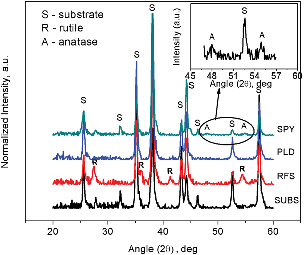
X-ray diffraction spectra of substrate and TiO2 films grown by three different techniques
Raman spectroscopy
The Raman active modes for anatase and rutile are A1g+B1g+B2g+Eg and A1g+2B1g+3Eg respectively. For rutile type TiO2, its features are at the values of 144 (B1g), 236 (Eg), 446 (Eg) and 610 (A1g). For anatase type TiO2, its Raman vibration modes are at 144 (B1g), 196 (B1g), 325 (Eg), 398 (Eg), 516 (Eg) and 638 cm−1 (A1g). In Fig. 2, the line marked RFS shows the Raman spectrum of TiO2 obtained by RFS. The spectrum consists predominantly of rutile phase. The new peak at 518 cm−1 corresponds to the nanocrystalline form of rutile phase.
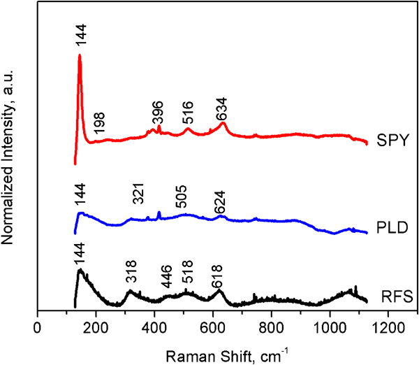
Raman spectrum of TiO2 thin film prepared by different techniques
The line marked PLD shows the Raman spectrum of TiO2 thin film prepared by PLD showing predominantly rutile peaks. The expected peaks around 516 and 638 cm−1 are shifted to 505 and 624 cm−1 respectively, indicating nanostructured growth. Further experiments are necessary to understand the shift and possible phase transformation to rutile phase. The other peaks at 377, 415, 747, 876 and 1067 cm−1 are expected to be from substrate.
The line marked SPY shows the Raman spectrum of TiO2 prepared by SPY technique of anatase phase. The extra peak at 446 cm−1 corresponds to the coexisting rutile phase.
Scanning electron microscopy
Figure 3 shows the SEM image of the films deposited on alumina substrate by RFS. A low magnification image is shown in Fig. 3a. The film is very dense, and the coating is uniform over the area of the substrate with large agglomerates formed due to morphology of the underlying alumina. Figure 3b shows the high magnification image. It can be observed that the agglomerates consist of fine nanoparticles of 15–20 nm size, which compares well with the grain size calculation from XRD peak broadening.
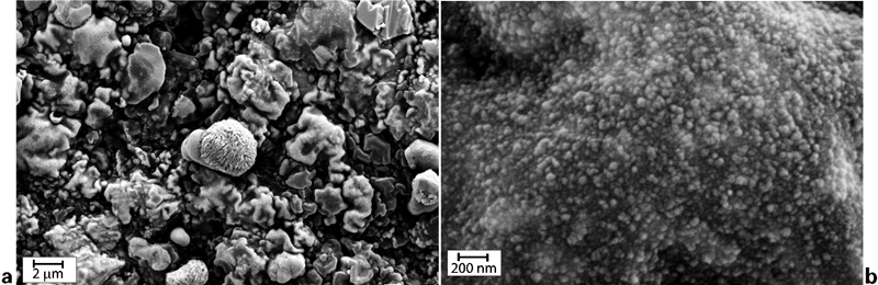
Image (SEM) of TiO2 thin films grown on alumina by RFS method a at low magnification and b at high magnification
Figure 4 shows the morphology of thin films grown on alumina by PLD technique at low and high magnification respectively. The film consists of wide range of particle size from 20 to 60 nm. Energy dispersive spectrum (EDAX) of the area confirms the presence of Ti and O atoms. Hence, it can be concluded that the region is amorphous with incomplete grain growth corroborating the absence of TiO2 crystalline peaks in XRD.
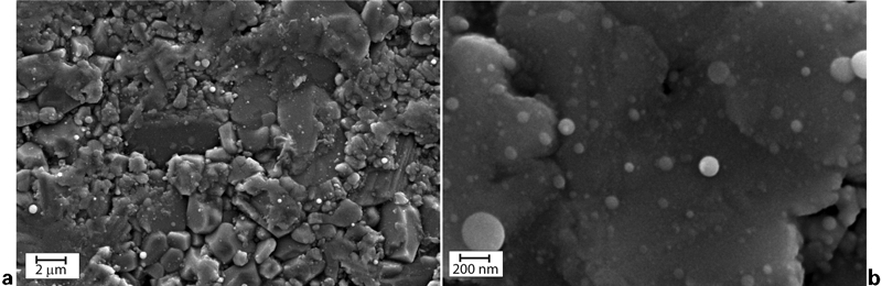
Image (SEM) of TiO2 thin films grown on alumina by PLD technique: a at low magnification and b at high magnification
Figure 5 shows the micrograph of films deposited by SPY. Figure 5a shows the low magnification image. As mentioned earlier, the film is uniform over the topography of the substrate and consists of fine nanoparticles. These nanoparticles possess a distinct shape in the form of elongated beads as shown in Fig. 5b. These nanobeads have a width of around 10 nm, which agrees well with XRD particle size determination and the average length of around 50–60 nm.
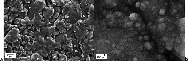
Image (SEM) of TiO2 thin films grown on alumina by SPY method: a at low magnification and b at high magnification
Nanoindentation
Nanoindentation studies were performed on films grown on Si (100) substrate. The film only hardness has been plotted for various deposition techniques, as shown in Fig. 6. It is observed that the films prepared by RFS technique shows higher hardness (23 GPa) than the other two techniques. This is due to denser films obtained by RFS technique involving atom by atom deposition, while in PLD, chunks of material are transported onto the substrate, leading to less denser films, and the SPY technique also deposits films with porosity. The hardness values are higher than those for single crystal and oriented rutile and anatase films reported in literature.21,22 The modulus of these films is in the range of 200–250 GPa.
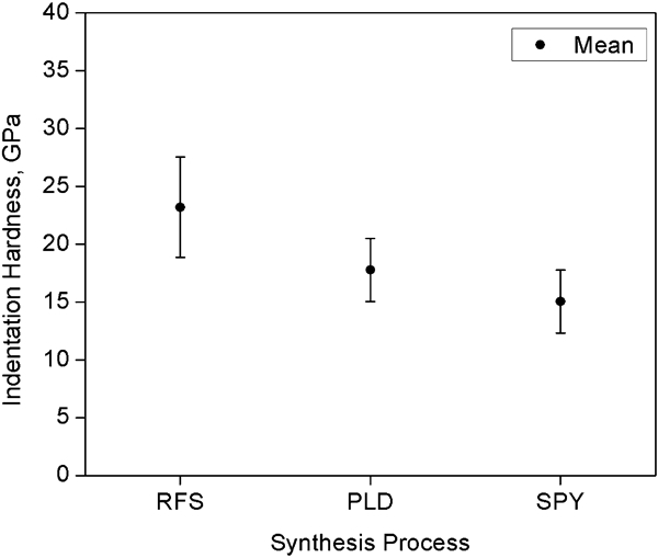
Hardness of TiO2 thin films deposited by various techniques
Ultraviolet-visible spectrophotometry
Ultraviolet-visible spectrophotometric experiments were performed on films grown on Si (100) substrate. The spectrum was recorded in reflectance mode. The absorption coefficient, α may be expressed as
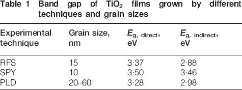
Band gap of TiO2 films grown by different techniques and grain sizes
When quantum confinement is present, the expression for band gap is derived by23
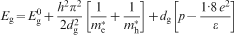
 denotes the band gap energy for the bulk material with large grain size (dg≫∞), m* terms are the electron and hole effective masses, e is the charge of the electron and ϵ is the dielectric constant and p represents the polarisation term.
The experimental values of the band gap obtained in this study follow the trend as represented by equation (3). The band gap of the material is found to decrease with increasing particle size. Consequently, there is a large shift from bulk values of band gap of TiO2 and that of nanocrystalline TiO2. Hence, a range of band gap can be obtained by suitably altering the processing methods and/or conditions. This affects the conductivity of the TiO2 films, which can be employed in obtaining tailor made films for gas sensing applications.
Conclusion
Thin films of TiO2 were grown by RFS, PLD and SPY techniques. The films as obtained through RFS showed rutile phase. The direct band gap was in the region of 3·37 eV. The films were composed of fine spherical nanoparticles of 15 nm sizes. The films fabricated through PLD technique were amorphous in as received state and possessed a direct band gap of 3·28 eV. The films prepared by SPY were of anatase phase. The direct band gap was around 3·5 eV. The morphology of films revealed the presence of nanobeads of 10 nm width and 50 nm lengths. Radio frequency sputtered films possess higher hardness and are denser than films prepared by PLD and SPY. Hence, by altering the processing technique, films of various microstructures are obtained. It is possible to obtain highly oriented films and specific morphology by performing various post-deposition processes. Spray pyrolysis offers a simple way of controlling shape and electronic properties of the thin films. Conductivity measurements are under progress to characterise the gas sensing behaviour of the films.
Footnotes
Acknowledgements
The authors would like to acknowledge F. Jose, N. C. Raut and R. Krishnan for the film synthesis and S. Kalavathi, V. Sivasubramaniam, M. Kamruddin (IGCAR) and Ankan Paria (IIT Kharagpur) for characterisation. The authors are also grateful for the encouragement and support from C. S. Sundar and Baldev Raj for his motivation and discussions.