
Abstract
Boron doping into diamond film can improve its conductivity and enhance its applications in electronic device, electrochemical and biomedical sensing devices. In the present study, boron doped diamond films were deposited on Si(100) using trimethylboron as a boron source by microwave plasma chemical vapour deposition with the B/C ratio in the gas mixture varying from 0 to 11 000 ppm. The boron doping resulted in the reduction in grain size of diamond and the increase in crystal imperfection. The number of twins in diamond grains increased for boron doped diamond films deposited at a high B/C ratio. Two new peaks at approximately 500 and 1220 cm−1 resulted from Fano interference in Raman spectra were observed and dominated for heavily boron doped diamond film. Boron doping into diamond films improved their field electron emission properties and remarkably reduced the turn-on electric field. The low turn-on electric field of 15·3 V μm−1 was achieved for boron doped diamond film deposited at B/C = 5600 ppm.
Introduction
Diamond is a wide band gap semiconductor material with extreme physical and chemical properties, such as the highest hardness and Young's modulus, the highest thermal conductivity, chemical stability, resistance to particle bombardment, negative electron affinity when hydrogen terminated on the surface, which makes it an excellent candidate for mechanical, field electron emission (FEE) devices, electronic and biomedical applications.1 Well adherent nanocrystalline diamond films were successfully deposited on pure Ti substrates and exhibited a low coefficient of friction and a negligible wear rate during sliding against a cemented carbide ball, which are of importance for tribology and biomedical implants.2,3 Recently, there has been a growing interest in diamond based electrochemical and biomedical sensor devices owing to its superior electrochemical properties.4 – 9 Compared with traditional carbon electrodes, such as glassy carbon and highly oriented pyrolytic graphite, diamond electrodes provide a very wide electrochemical potential window in aqueous media, low and stable background current, chemical stability, corrosion and fouling resistance, good compatibility and self-cleaning effect. Therefore, the planar boron doped diamond film electrode is an alternative to traditional carbon electrodes, and has been recognised as one of the most promising electrode materials to achieve higher sensitivity, selectivity and lower detection limit for sensing applications.
Apart from electrochemical applications, the diamond film is considered to be a highly promising field emission cold cathode material due to its highly stable negative electron affinity.10 – 13 The microstructure and morphology of a diamond film have an important effect on the field emission properties of diamond. The deposited globe-like diamond microcrystalline aggregate films by microwave plasma chemical vapour deposition exhibited excellent electron emission properties and stability.14 Diamond in nanocone geometry had been shown capable of reducing the turn-on field to 6 V μm−1,11 which was comparable to that of carbon nanotubes. However, the fabrication process of the particular surface geometries of diamond is complicated. The FEE properties of diamond also can be improved by introducing boron, nitrogen and phosphor atoms into diamond.15,16 The doping could be achieved through ion implantation and in situ chemical vapour deposition diamond film growth as well as via forced diffusion.17 With the development of chemical vapour deposition technique, the doping through in situ growth has become the most important doping method. The doped atoms can change the valence band structure of diamond. The defect or impurity levels are formed due to the existence of defects and impurities in diamond, which facilitates the electronic transmission and excitation, resulting in strong field emission. In comparison with nitrogen and phosphor atom, boron atom is currently easily doped into polycrystalline and nanocrystalline diamond films and used as an acceptor due to its small atomic radius. The doping of boron atoms in polycrystalline diamond films has been observed to reduce the threshold electric field for electron emission.18,19
Therefore, the boron doped diamond films have become the focus of research as cold cathode materials in FEE to realise the industrial applications aimed for flat panel displays and cold cathodes of microelectronics. Although the study of the field emission characteristic of diamond has made remarkable progress, the search for the improvement of FEE properties of diamond by element doping is still a focused research area. The growth and characterisation of boron doped diamond films are of considerable interest and practical application value, especially in field electron display industry. In this work, the authors deposited boron doped diamond films at different B/C ratios in the gas mixture by microwave plasma chemical vapour deposition using trimethylboron (TMB) as a boron source. The influences of boron doping on the growth characteristics, surface morphology and microstructure, as well as the FEE properties of boron doped diamond films were systematically investigated.
Experimental
The boron doped diamond films were deposited on mirror polished Si(100) substrates using microwave plasma chemical vapour deposition system with a 1·5 kW microwave generator. The substrates were precleaned ultrasonically in acetone and ethanol for 10 min. Then they were ultrasonically abraded for 60 min in a suspension of mixed diamond powders with a grain size of 5 nm and 3 μm in ethanol to obtain a high nucleation density. Next, they were again ultrasonically cleaned in deionised water to remove the diamond particles sticking to the substrate surface and dried in nitrogen gas blow before being inserted into the reactor chamber. The TMB was used as a boron source, which was diluted by H2 to 1000 ppm. The plasma was induced in gas mixture of 0·5%CH4–99·5%(H2,TMB) with a microwave power of 1200 W at total pressure of 30 torr and a total gas flow rate of 200 sccm. The diamond films with different boron concentrations were deposited by adjusting the B/C ratio in the gas mixture varying from 0 to 11 000 ppm. The substrate temperature was ∼800°C and directly measured by an optical pyrometer through a sapphire window. The deposition duration for all the boron doped diamond films was 8 h. The microstructure and surface morphology of the deposited boron doped diamond films were characterised by visible Raman (spot size: 1 μm; wavelength: 514·5 nm) spectroscopy and scanning electron microscopy (SEM; Philips 30 XL FEG). The FEE properties were measured in ultra high vacuum automatic scanning probe system with the vacuum of 10−6 Pa. The distance between the diamond sample and anode (scanning probe) was controlled through the stepper motor by a computer, and kept at 50 μm when measuring.
Results and discussion
The boron doped diamond films with different boron concentrations were prepared by adjusting the B/C ratio in the gas mixture. Figure 1 shows the surface morphology of the boron doped polycrystalline diamond films deposited at the B/C ratio of 0, 800, 2000, 5600, 8800 and 11 000 ppm. Those SEM images demonstrate that the surface morphologies are dependent on the B/C ratio in the gas mixture. The polycrystalline diamond films deposited at a B/C ratio less than 800 ppm show the clear crystal facet, uniform grain size of about 1–2 μm, and clear grain boundaries between grains, as shown in Fig. 1a and b. When the B/C ratio increases to 2000 ppm, the diamond grains begin to lose the characteristic of clear crystal facets, and the grain size becomes inhomogenous, as shown in Fig. 1c. Meanwhile, there is a large number of secondary nucleation on the diamond grain surfaces. Further increasing the B/C ratio to 5600 and 8800 ppm, well faceted diamond crystallites are gradually degenerated as well as the density of secondary nucleation increasing. The ridges and steps oriented parallel to one other are observed in the diamond grains, representing the feature of twinning bands within the grains intersecting with the surface, which is associated with the abundant boron atoms. When the B/C ratio further increased to 11 000 ppm, the heavily boron doped diamond film was obtained. The diamond grain size refined to below 1 μm due to the high secondary nucleation density, as shown in Fig. 1f.
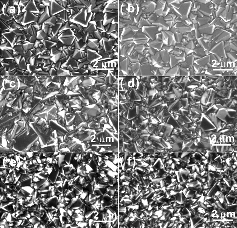
Surface SEM image of boron doped diamond films deposited at different B/C ratios
Figure 2 shows the cross-section SEM image of diamond films deposited at different B/C ratios in the gas mixture. It demonstrates that all the boron doped diamond films exhibit columnar growth and have column structure. The deposited boron doped diamond film was very dense, and no gaps were observed between the diamond and the substrate, indicating very good adhesion of the diamond film. By measuring the thickness of the deposited diamond films according to the cross-section SEM images, the growth rate of the film was determined, as shown in Fig. 3. With increasing the B/C ratio, the growth rate of diamond films decreases significantly at the B/C ratio below 2000 ppm, and then decreases slightly when the B/C ratio increases from 2000 to 11 000 ppm. The growth rate was reduced to be ∼0·17 μm h−1 for the boron doped diamond films deposited at a B/C ratio of 11 000 ppm. With the addition of TMB in the gas mixture, the plasma composition and chemical reaction have been modified, especially the decrease in H/H2 and CH/H ratios in the plasma. For the polycrystalline diamond growth, the CH radical is dominant growth species, and the growth rate is limited by hydrogen abstraction reactions at the diamond surface.20 Meanwhile, the doped boron atoms can terminate the growth sites and inhibit the further growth of diamond in the diamond growth process. Therefore, the growth rate of diamond decreased with increasing the B/C ratio. However, it was reported that the phosphorus or nitrogen atom promoted the diamond growth and resulted in the increase in growth rate for the phosphorus or nitrogen doped diamond films.21
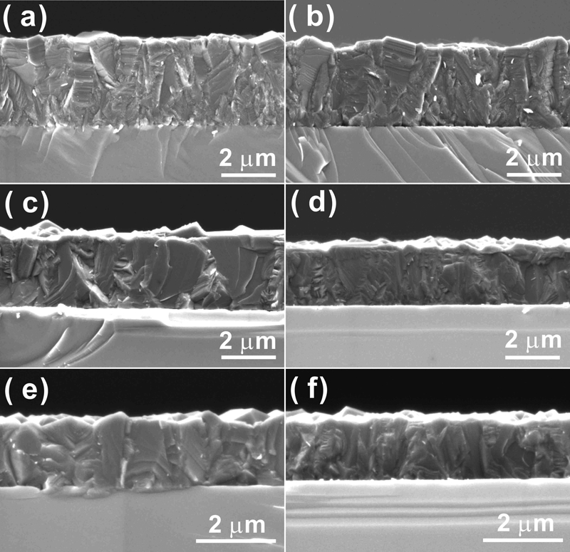
Cross-section SEM image of boron doped diamond films deposited at different B/C ratios
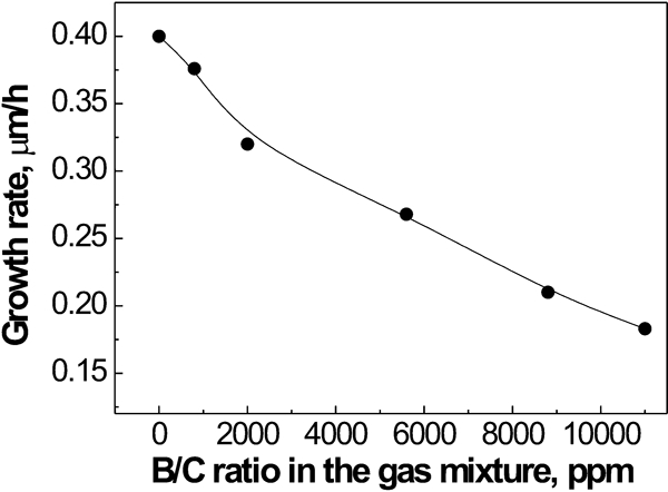
Growth rate of boron doped diamond films deposited at different B/C ratios
Figure 4 shows the visible Raman spectra acquired from the boron doped diamond films deposited at different B/C ratios. As shown in Fig. 4, the characteristic silicon substrate vibrations at 519 and 970 cm−1 were also observed due to the small thickness of the boron doped diamond film, besides the characteristic peak of diamond in the visible Raman spectra. The results reveal that the peak intensity at 1332 cm−1 of the deposited diamond films decreases, and the peak position shifts to lower wavenumber with increasing the B/C ratio in the gas mixture. For the undoped diamond film, the diamond phonon observed at 1332 cm−1 is a symmetric Lorentzian. However, for the boron doped diamond films, the asymmetry of diamond peak in visible Raman spectra appears and becomes more apparent with the increase in B/C ratio. When the B/C ratio increases to 5600 ppm, a new wide band arises at ∼1220 cm−1. As the B/C ratio further increases, the intensity of the peak located at ∼1220 cm−1 also increases. At the B/C ratio of 11 000 ppm, the asymmetry of diamond characteristic peak was further enhanced, and an obvious new peak at ∼500 cm−1 was observed. Moreover, the broad peaks located at around 500 and 1220 cm−1 become the main features in the boron doped diamond film, as shown in Fig. 4f. Studies have indicated that the asymmetry of diamond characteristic peak and the emergence of the broad peaks at approximately 500 and 1220 cm−1 are due to Fano interference effect as a result of boron doping in diamond films.22 The Fano interference is caused by quantum mechanics interference between the zone centre Raman active optical phonon and the continuum of electronic states induced by the presence of the dopant.
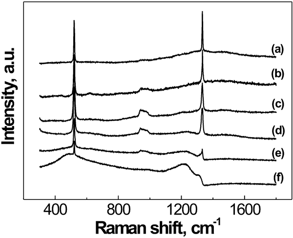
Visible Raman spectra of boron doped diamond films deposited at different B/C ratios
In boron doped diamond films, boron atoms substituted for partial carbon atoms and were incorporated into substitution sites. Because the number of valence electron of boron atom is one fewer than that of carbon atom, the boron atom would capture an electron from surrounding carbon atom to form the stable covalent bond structure. The substitution of boron atoms for carbon atoms results in the lattice distortion and the damage of symmetry as the radius of boron atom is slightly larger than that of carbon atom. Therefore, some defects, such as microtwins and stacking faults, appear when boron atoms replace carbon atoms and occupy the lattice sites of diamond, and the number of defect increases with the increase in B/C ratio. The gradual change in the Raman spectra also indicated that the microstructure of the boron doped diamond films was affected by boron doping. For heavily boron doped diamond films, the peaks located at 500 and 1220 cm−1 dominate the Raman spectrum because the Fano parameters saturate and it becomes difficult to discern the position of the zone centre phonon. Furthermore, the peak located at 500 cm−1 can be fitted with a combination of Gaussian and Lorentzian line shapes, and the fitted centre wavenumber can be used to estimate the content of boron atoms in the heavily boron doped films according to the following equation23

Diamond film is an ideal field emission material due to its negative electron affinity. The field electron emitting properties of the diamond films and the effect of B/C ratio on the FEE properties were investigated. Figure 5 shows the dependence of the emission current density on the applied electric field for the diamond film without boron doping, the boron doped diamond films deposited at B/C = 5600 ppm and 11 000 ppm. The results indicated that the turn-on electric field corresponding to an electron emission density of 0·01 mA cm−2 of diamond film varied significantly with the boron doping level. The turn-on electric fields were measured to be 25·0, 15·3 and 17·4 V μm−1 for the diamond film without boron doping, boron doped diamond film deposited at B/C = 5600 ppm and heavily boron doped diamond film deposited at B/C = 11 000 ppm respectively. The undoped diamond film exhibited high turn-on electric field for electron emission due to its insulation nature. Compared with the undoped diamond film, the FEE properties of diamond films are improved through boron doping. For the boron doped diamond film deposited at the B/C ratio of 5600 ppm, the turn-on electric field remarkably decreases as a result of the modification of film surface morphology, the introduction of defects and the decline of work function resulted from the doped boron atoms. However, the FEE property shows no further improvement for the heavily boron doped diamond film deposited at B/C = 11 000 ppm. On the contrary, the turn-on electric field increases to 17·4 V μm−1 for the boron doped diamond film deposited at B/C = 11 000 ppm, although the film has much higher conductivity. It is ascribed to the electron trapping of the heavily boron doped diamond film, which demonstrates the hole conduction rather than the electron conduction. The acceptor states can trap the electrons and result in a higher turn-on electric field for the heavily boron doped diamond film.24 Fowler–Nordheim theory is usually used to analyse the results of FEE. Figure 6 shows the corresponding Fowler–Nordheim curves of the diamond film deposited at different B/C ratios. The data follows the linearity of ln(J/E2) versus 1/E plot, which indicates the electron emission follows the FEE mechanism of a quantum mechanical tunnelling over a barrier.
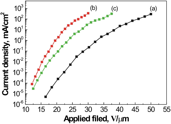
Field electron emission properties of boron doped diamond films deposited at different B/C ratios
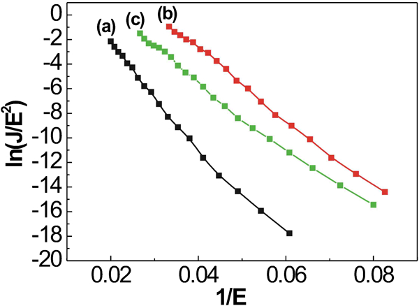
Corresponding Fowler–Nordheim plots of ln(J/E2) versus 1/E for boron doped diamond films deposited at different B/C ratios
Conclusions
The boron doped polycrystalline diamond films were prepared by microwave plasma chemical vapour deposition systems in the gas mixtures of CH4–H2–TMB using TMB as a boron source with the B/C ratio varying from 0 to 11 000 ppm. The boron doping resulted in the degradation of clear crystal facets of diamond grains, the reduction in grain size and increase in defects. The doped boron atoms terminated the diamond growth sites and inhibited the further growth of diamond. The number of twins in diamond grains increased for the boron doped diamond film deposited at a high B/C ratio. It was found that the asymmetry of diamond characteristic peak in the visible Raman spectra was enhanced at a high B/C ratio, and two new peaks located at approximately 500 and 1220 cm−1 which resulted from Fano interference appeared and dominated for the heavily boron doped diamond film. The FEE properties of the boron doped diamond films were observed to be remarkably superior to that of the undoped diamond film, and can be tuned by controlling the boron atom concentration in the diamond film. The low turn-on electric field of 15·3 V μm−1 was obtained for the boron doped diamond film deposited at B/C = 5600 ppm.
Footnotes
Acknowledgements
This work was financially supported by the Natural Science Foundation of Jiangsu Province of China (grant no. BK2008419) and PhD Programs Foundation of the Ministry of Education of China for Young Teachers in University (grant no. 200802881003). Support from the NUST Research Funding (project no. ZDJH07) is also gratefully acknowledged.