
Abstract
Precision injection moulding of miniaturised products with microfeatures, such as channels for microfluidic applications, poses the greatest challenges in terms of tooling technology and process optimisation. The injection moulding process window of polypropylene was validated using a metrological approach for the production of a microfluidic substrate. The dimensional accuracy of microchannels that are 48 μm wide and 110 μm deep and the quality surface topography replication (surface roughness from 30 to 360 nm) were investigated using non-contact measuring instruments, such as an optical coordinate measuring machine and a white light interferometer respectively. The effect of the dimensional scale range on the micro-/nanofeature replication was evaluated, and it was found to be the dominant parameter if compared with the effect of the other process related parameters investigated (melt and mould temperatures and injection speed).
Introduction
Applications of polymer based microfluidic systems cover a broad range of devices with different functions, such as capillary electrophoresis, deoxyribonucleic acid analysis, cell handling, microreactions, clinical chemistry and diagnosis.1 The latter category is of great interest and takes advantage of the mass fabrication capability of replication processes, such as injection and microinjection moulding. In order to avoid contamination from different biological samples, disposable devices are needed for this application.
The dimensional accuracy of microchannels is of great importance in microfluidic systems. The fundamental measuring tasks to be performed in the quality control of microfluidic systems are the width (define as the distance between two opposing surfaces) and the depth (defined as the distance between two surfaces of the same orientation but placed in a vertical direction) of a microchannel.2 A microchannel's width and depth must comply with the dimensional specifications in order to be able to contain the correct volume of reagents and biological fluids to be analysed and to convey the requested flowrate designed for the function to be delivered. Surface topography is also of great importance in polymer microfluidics; hence, the replication capability of the process and the surface quality of the tool have to be evaluated and possibly optimised. The surface finish on microfluidics has different roles, depending on the location on the surface device. First, low roughness is required to allow the assembly by laser welding of a lid on top of the microfluidic unit for sealing purposes and, second, to diminish the interaction between the biofluid to be analysed and the channel/reservoir surfaces.
In the present paper, the precision moulding of a microfluidic system for blood analysis was analysed and validated using a metrological approach applied to both microchannel dimensions (width and depth) and to surface topography on a reservoir chamber and on the microfluidic substrate surface. The dimensions were measured using an optical coordinate measuring machine (CMM); optical profilometry, such as white light interferometry (WLI), was used for the topographic characterisation of polymer surfaces. Optical techniques provide fast non-contact measurements, which are, in general, recommendable when inline process controls are needed on soft materials and when sample contaminations are to be avoided.
Micromanufacturing
A key issue in biomedics is the realisation of convenient, easy to implement and disposable microfluidic systems, in particular for blood processing and analysis. For this purpose, different designs based on microchannel bend structures have been proposed and developed.3 One of these devices has been selected as a benchmark for the present study (Fig. 1). In the chosen microfluidic system, the function of separating blood from plasma is delivered by two different and concurrent mechanisms: a centrifugal force field due to the bent microchannel (resulting in different settling velocities between particles and the surrounding fluid) and a ‘plasma skimming effect’, which was observed at the microscale at bifurcating capillary vessels. Separation originates at the bifurcation point due to the different flowrates on the two branches (i.e. microchannels; Fig. 1) and the presence of sharp edges (i.e. very small fillet radius of 25 μm): particles tend to enter the branch with higher flowrate. The final result is an uneven haematocrit distribution in the two channels after the bifurcation.
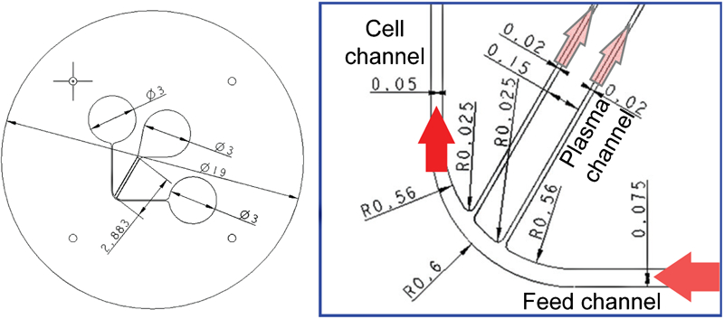
Microfluidic system for blood analysis: layout, nominal dimensions and working principle4
It is clear that for the proper functioning of the system, the roughness and geometry of channels and surfaces have to be finely controlled. Such requirements pose the greatest challenges in terms of tooling technology, injection moulding replication capability and process optimisation. Tooling process chain and injection moulding experiments are described in the following sections.
Tooling
With increasing trend towards miniaturisation and integration of different microfeatures, only a combination of processes can lead to the accurate manufacture of micromoulds. The concept of hybrid tooling was therefore introduced and applied. Hybrid tooling can be defined as ‘the capability of producing a mould insert combining two or more processes in sequence (i.e. on the same process chain for tooling)’.5 The term indirect machining covers the fact that the master structure produced by machining is the positive geometry, which is identical in shape to the final product (i.e. the opposite of what is needed for the actual mould insert).6
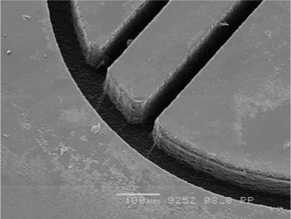
An innovative process chain based on indirect hybrid tooling was developed and implemented. Microelectrical discharge machine (μEDM) milling was selected as the starting micromachining process. The material substrate (or master) needed to be suitable for both μEDM milling (to be conductive or semiconductive) and selective etching after the electroforming is completed. Because of the microfluidic application, it was preferable to have a flat and smooth substrate surface to ease the sealing during the packaging of the final product (i.e. bonding of a lid on top of the microfluidic system). For these reasons, an 8 in. silicon wafer (1000 μm thick) was used as substrate to be machined by μEDM milling. The process chain was composed by the following steps (Fig. 2):7 μEDM of microstructures on the silicon substrate (master), pretreatments including cleaning and deposition of a thin layer of Ti/Cu by physical vapour deposition coating, electroforming of nickel and copper for the insert fabrication, selective etching of silicon in a warm alkaline solution, mechanical machining of the back of the insert and of the external shape, final cleaning and selective etching of the Ti/Cu layer (see nickel microtool detailed views in Fig. 3).
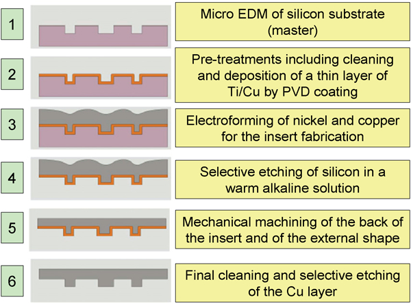
Microtool manufacturing by hybrid tooling process chain7
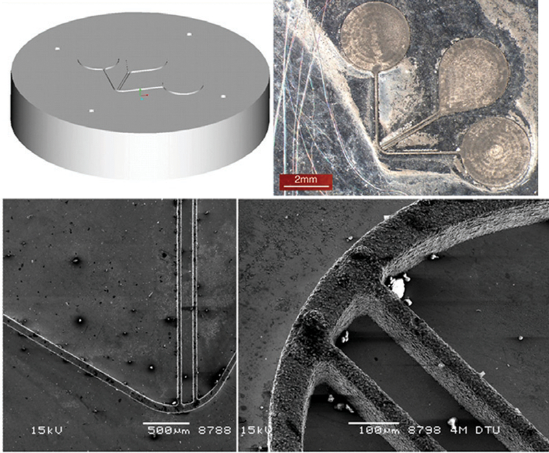
Microtool fabricated by hybrid tooling8
Injection moulding
Polymer microfluidic chips were injection moulded using a commercially available polypropylene grade provided by Basell and produced by means of a series of statistically designed injection moulding experiments. The injection mouldings were executed on a conventional injection moulding machine with a reciprocating screw of diameter of 35 mm and a clamping force of 60 t. During the design of experiment (DOE) phase, three process parameters have been controlled: temperature of the melt, temperature of the mould and injection speed. The process parameters were varied between two levels, resulting in a full factorial three-factor two-level experimental design (23 = 8 experiments). The process levels were set as follows:
Tmelt(max) = 260°C was selected following the recommendations from the material supplier in order to avoid polymer overheating and subsequent material degradation, especially due to the residential time in the barrel in the period between two consecutive moulding cycles
Tmelt(min) = 220°C was selected following the recommendations from the material supplier in order to obtain an effective polymer melt flow and as a consequence effective replication and stable process realisation
Tmould(max) = 75°C was set following the recommendations from the material supplier in order to allow successful demoulding of the part from the cavity and at the same time performing the injection process within a suitable cycle time (i.e. short cooling time)
Tmould(min) = 55° was the lowest temperature allowing microfeature replication and complete filling of the cavity at the slowest injection speed
InjVel(max.) = 350 mm s−1 was limited by the capability of the machine in terms of clamping force capable of withstanding the injection pressure developed at such injection speed (i.e. avoiding flashes and distortions)
InjVel(min.) = 150 mm s−1 was the minimum speed providing effective replication at low melt and mould temperatures respectively.
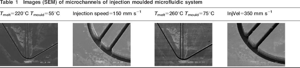
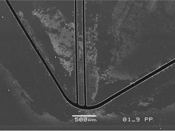
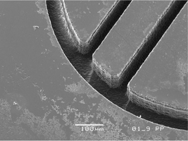
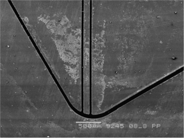
The focus of the experiments was to validate the process windows for the injection moulding of polymer microfluidic systems with regards to surface topography characteristics and dimensional replication of microchannels. First, a preliminary inspection of the parts was carried out for a qualitative validation of the process window. For this purpose, light optical microscopy and scanning electron microscopy (SEM) were employed (Fig. 4 and Table 1). Scanning electron microscopy in particular was applied in order to obtain high resolution and high magnification images of the microstructures. Subsequently, surface topography measurements using WLI and dimensional measurements using an optical CMM were performed to carry out a quantitative investigation of the replication capability of the injection moulding process in the selected process window.
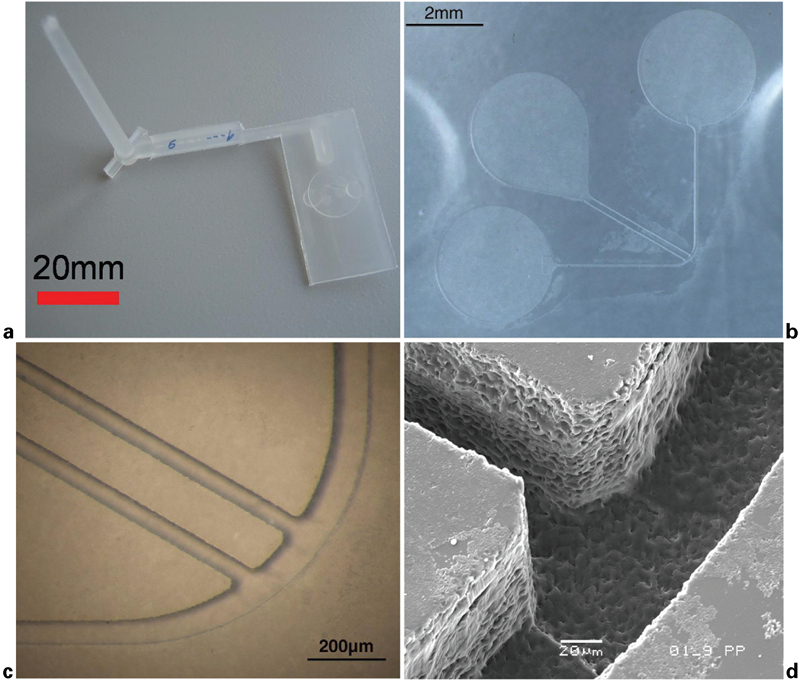
Blood/plasma separation unit of microfluidic system produced by injection moulding (material = polypropylene)
Images (SEM) of microchannels of injection moulded microfluidic system
Dimensional measurements
The width at the top of the microchannels (corresponding to the width at the base of the walls in the tool) and the depth of the microchannels (corresponding to the height of walls in the tool) were chosen as measurands for process validation. Measurements were carried out with an optical CMM, which is a non-contact instrument suitable for measurement on soft materials (i.e. polymers). It also allows fast measurements, which makes it suitable for inline quality control. For both vertical and horizontal measurements, a comprehensive uncertainty budget was created following the method derived from the ISO-GUM 9 , 10 and here extended to sub-100 μm features including not only the measuring equipment (machine calibration for microscale measuring range, resolution, measuring repeatability and focusing procedure) and workpiece (temperature effect, alignment and measurand definition) but also the injection moulding process (process window, process variability and production repeatability).
Measurement variations due to different sources were calculated as standard deviation for both height and width dimensions (Table 2):
Measuring uncertainty and different sources of measurement variation
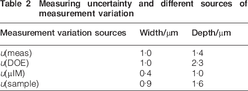
instrument repeatability [u(meas)]: repeated measurements on the same spot of the same specimen
process window span [(u(DOE)]: measurements related to the eight different experimental designs
injection moulding process variation [u(μIM)]: measurements on five different specimens produced under the same processing conditions
sample variation [u(sample)]: measurements on three different locations on the same sample.
The uncertainty of dimensional measurements was assessed and implemented on the statistical analysis. After measurement variation contributors, other sources of uncertainty were taken into account and are listed as follows:
instrument calibration [u(cal,cmm)]: the instrument was verified by performing repeated measurements on artefacts, such as a calibrated optical scale for horizontal (i.e. X and Y) measurements and a calibrated step
u[cal,cmm(x, y)] = 0·85 μm
u[cal,cmm(z)] = 2·1 μm
artefact calibration uncertainty [u(cal)]: the calibration of the reference artefact is provided by the manufacturer and reported in the calibration certificate
u[cal(x, y)] = 0·25 μm
u[cal(z)] = 0·20 μm
uncertainty due to the temperature [u(temp)]: the temperature related standard uncertainty was calculated for a maximum temperature variation of ±2°C (assuming a rectangular distribution) and using a coefficient of linear expansion for polypropylene of α = 110×10−6/°C

The combination of all the contributors listed in Table 2 gives as result the combined manufacturing standard uncertainties, calculated using the error propagation law as described in the ISO-GUM standard,9 where y is the measurand, n is the number of uncertainty contributors, f is the model function of the measurement and u(xi) is the standard uncertainty of the ith uncertainty contributors.
Once applied to the above mentioned uncertainty budget, the final expanded uncertainty results in the following


Results are reported in Figure 5 Figs. 5 and 6, where the effects of the variations within the respective limits of the three controlled process parameters (injection speed and melt and mould temperatures) are graphically summarised. The graphs show how variations of process parameters within their limits produced only slight variations on the replication geometry. Therefore, the investigated process window was validated: in the entire processing condition range, conformance between the injection moulded part and the microtool was found, particularly when the uncertainty was taken into account. The optimised conventional injection moulding (which is needed to provide relatively large shot volume to mould millimetre sized parts) produced fully replicated high aspect ratio microfeatures, such as 48 μm wide (Fig. 5) and 110 μm deep microchannels (Fig. 6). All the process parameter combinations led to features in the polymer component having dimensions completely compatible with the respective dimensions in the tool.
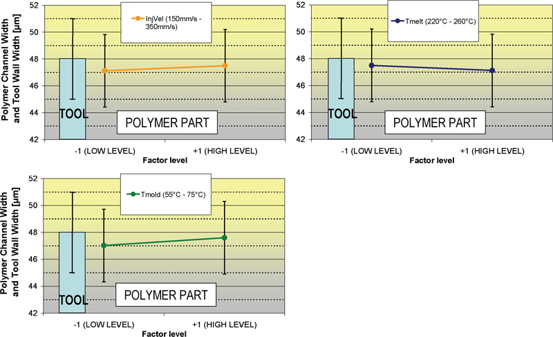
Replication capability in terms of microchannel width (bars represent expanded uncertainties): main effects plot of three investigated process parameters on average polymer channel width compared with corresponding dimension (width) on tool
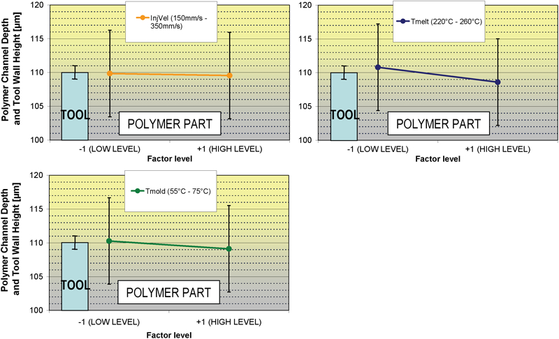
Replication capability in terms of microchannel depth (bars represent expanded uncertainties): main effects plot of three investigated process parameters on average polymer channel depth compared with corresponding dimension (height) on tool
Surface topography characterisation
Owing to the hybrid micromanufacturing technology employed for the tool making process, two different types of surfaces were obtained within the microcavity:
the polymer chip substrate surface, having a finely finished flat surface, with a roughness Ra<100 nm, realised by nickel–copper electroforming and selective etching of a silicon master
the microchannels and reservoir chambers surfaces, with a roughness Ra in the range of ∼500nm, realised by nickel–copper electroforming and selective etching of the silicon substrate machined by μEDM (microelectrodischarge machining).
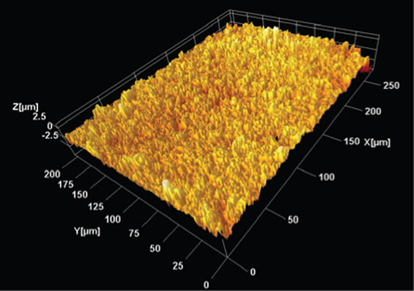
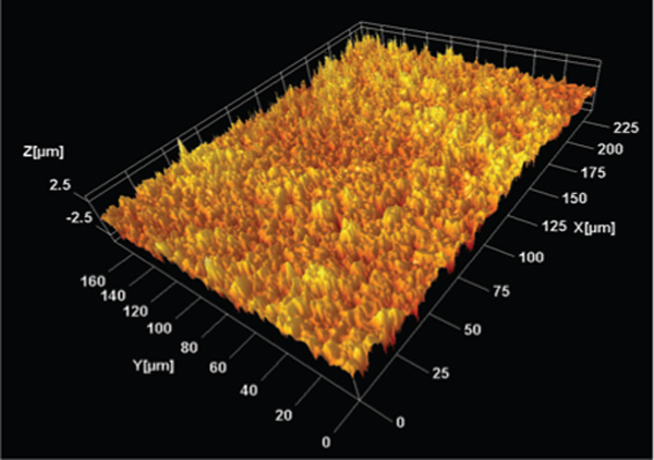
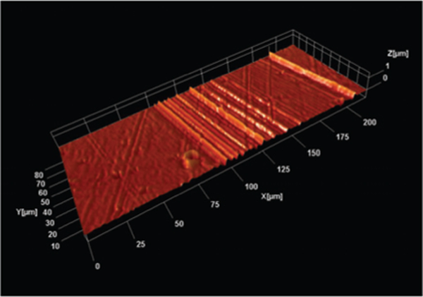
White light interferometry was employed to map the surface topography generated by the injection moulding process at different injection conditions on different positions, located on both areas indicated in Fig. 7: surface inside the reservoir chamber and surface of the microfluidic platform substrate.
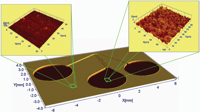
White light interferometry scanning on two selected regions on polymer microfluidic system: polymer chip substrate surface (left) and reservoir chamber surface (right)
Measurement strategy and equipment
White light interferometry is a powerful technique for surface profilometry, allowing contactless reconstruction of topography and quantitative characterisation of surface roughness. White light interferometry allows fast and accurate measurements and is therefore a suitable technology for inline quality control of surface topography. For the present study, a commercial instrument was applied, implementing a Mirau configuration, best suited for measurements with high magnification objective lenses. A scheme of the instrument is given in Fig. 8: it includes a Mirau interferometer objective, a motorised stage, a charge coupled device camera and a white light source. A beam splitter and a reference plate are placed inside the microscope objective: the beam reflected off the measured surface and the reference beam reflected by the reference plate form an interferogram, i.e. an interference pattern of light and dark fringes. The analysed sample is moved vertically with nanometre accuracy by a piezoelectric stage, thus producing phase shifts in the interferograms. Sensing the coherence peak during the vertical scan allows the calculation of a topographic surface map.
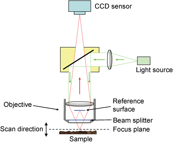
White light interferometer scheme
The instrument used in connection with the present work implements a ×50 objective, with a numerical aperture of 0·55 and a working distance of 3·4 mm. Such objective allows measurements over an area of 276×205 μm with a lateral resolution of 0·37×0·43 μm and a maximum detectable slope of <25°. The system provides measurements over a vertical range of 100 μm with a vertical scan speed of 2·1 μm s−1 and a vertical step size of <0·1 nm. In order to analyse the influence of process parameters on surface replication of the microinjection moulded parts, a three-dimensional investigation was carried out with the WLI technique. In particular, the average roughness Ra was chosen as a representative parameter to be analysed by means of DOE.
The WLI was equipped with a five-degree of freedom stage, which, together with the charge coupled device camera, helped the proper installation of the sample to be investigated. The set of microchannels was used as a reference system for the accurate positioning and orientation of the objective on different microparts. This was a fundamental requirement in order to measure the same surface regions obtained with different process conditions. The surface roughness was measured on four different positions: two lying on top of the microfluidic platform and two on the reservoir chamber. For each of the right process setups of the full factorial DOE, two samples were randomly selected from the production batch and measured. A total of 64 scans were carried out. Each measurement covered an area of 276×205 μm with a sampling of 752×480 pixels. The same measuring setup and strategy were adopted to measure the tool surface in the corresponding surface as in the polymer part.
After the measurement, the data sets were post-processed in order to isolate roughness from waviness and form contributions. Extending the approach proposed by the ISO 11562 standard13 for analysis of surface profiles, a Gaussian filter was applied on the scanned topographies.
Calibration
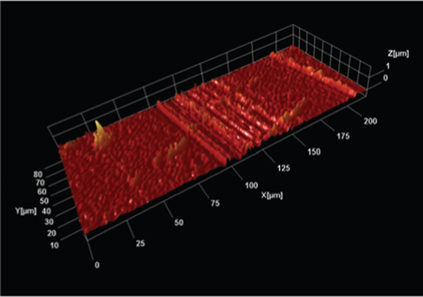
The WLI was implemented for the estimation of the average roughness Ra: since such a parameter is determined by local topography vertical deviations, it is important to verify the performance and calibrate the z scan system of the instrument. Calibration was carried out by measuring two calibration gratings, which featured a one-dimensional array of rectangular SiO2 steps on a Si wafer substrate, normally implemented for the calibration of scanning probe microscopes. Five measurements were repeated over a range of 86·32×64·20 μm, with a 752×480 pixel sampling on two reference standards, featuring 104·0±1·5 and 540±2nm high steps respectively (see scanning results in Fig. 9). In order to comply with the similarity principle, a polymer grating with comparable surface finishing would have been desirable; however, silicon reference standards are more commonly employed for calibration due to their accurate manufacturing process and time stability and were therefore to be preferred.
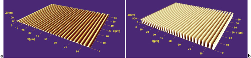
White light interferometry scanning on two TGZ type calibrated gratings (magnification factors: X direction = ×1; Y direction = ×1; Z direction = ×10)
Two methods are normally implemented for the calibration and determination of vertical scaling factors: the histogram method and ISO 5436.14 Both methods provide similar results that usually agree within the uncertainty limits. Since optical methods are particularly sensitive to edge regions,15 where surface regions with relatively high slopes are encountered, the ISO 5436 method was chosen. The method prescribes to exclude discontinuity areas from computation, and it is depicted in Fig. 10. Extending the analysis to the whole scanned areas, it is possible to determine the average scaling factor cz as the ratio between the measured height and the reference value
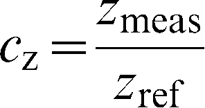
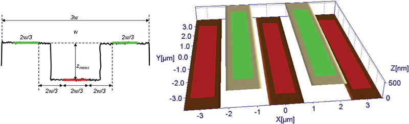
Illustration of step height determination according to ISO 5436: central parts of structure top and bottom terraces, equally spaced from edges, are taken into account to measure step height, whereas edge regions are left out of computation
One of the critical factors that typically affect the goodness of optical profilometer measurement is the installation slope. Indeed, the five-degree of freedom stage allows positioning of the sample relative to the objective axis with a maximum deviation from the perpendicular direction smaller than 0·4° but nevertheless apparently increases the estimated roughness. This can be associated first to the non-optimised illumination of the analysed surface and second to the increased number of points locally overcoming the maximum detectable slope (i.e. void pixels) determining the roughness measurement overestimation.16
In order to estimate the sensitivity to the installation slope, measurements were taken at increasing average relative angles, from 0·1 up to 2°, considering tilts around the x axis, y axis and the two combined. The results are summarised in Fig. 11. The average deviation due to installation slope was then extrapolated assuming a linear dependence. Since the average slope for the microfluidic system was estimated to be of 0·21°, a final deviation of about 1·1% of the measurand was calculated.
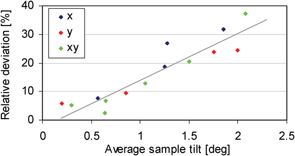
Effect of installation slope on estimation of average roughness Ra: different markers refer to rotation around two axes x, y and combined xy; independently from tilt axis, larger is slope of sample relative to objective axis, higher is relative deviation from average roughness
White light interferometry measurements uncertainty
The uncertainty of roughness measurements was assessed and implemented on the statistical analysis to verify the reliability of the obtained results. In the following, the considered contributors and the related average standard uncertainties in the measurements of the micromoulded part with the WLI are presented and discussed.
Instrument vertical calibration uncertainty [u(z)]: The instrument calibration was verified by performing repeated measurements on calibration gratings, which feature one-dimensional arrays of rectangular SiO2 steps on a Si wafer substrate, with two different step heights, i.e. 104·0±1·5 and 540±2 nm (Fig. 9). The two step heights have been selected because they represent the two roughness ranges encountered on the two different investigated areas. Vertical calibration standard uncertainty was estimated by calculating the standard deviation over five measurements on each calibration grating:
u(z,100 nm) = 0·5 nm (corresponding to 0·43% of the grating calibrated vertical range)
u(z,500 nm) = 0·9 nm (corresponding to 0·16% of the grating calibrated vertical range).
Grating calibration uncertainty [u(cal)]: The grating calibration uncertainty values are provided by the manufacturer with a coverage factor of k = 2 (corresponding to a confidence level of ∼95%); therefore, the standard calibration uncertainty is calculated as follows:
u(cal,z,100 nm) = 0·75 nm
u(cal,z,500 nm) = 1·0 nm.
Uncertainty due to background noise [u(noise)]: Repeated measurements on a silicon flat were performed in order to determine the background of the instrument; u(noise) was estimated by calculating the mean value of the average roughness Ra measurements on the silicon flat
u(noise) = 0·3 nm.
Repeatability of the measuring process due to the instrument [u(rep,meas)]: The measurement repeatability was estimated by performing 10 measurements on the same polymer specimen and on the same position and calculating the standard deviation of the measured average roughness values:
u(rep,meas) = 0·28% of the measurand (for the chip platform surface)
u(rep,meas) = 0·34% of the measurand (for the reservoir chamber surface).
Repeatability of the measuring process due to the relocation of the measurement area [u(rep,reloc)]: The measurement repeatability due to relocation was estimated by repositioning the WLI objective on the same sample with shifts of a few tens of micrometres nine times in order to simulate the effect of position accuracy on the Ra measuring result. The standard deviation of the measured average roughness values was calculated and used as estimate of u(rep,reloc) as follows:
u(rep,reloc) = 1·3% of the measurand (for the chip platform surface)
u(rep,reloc) = 1·1% of the measurand (for the reservoir chamber surface).
Uncertainty of the microinjection moulding process [u(μIM)]: The deviation of measurements on two different samples from the same production batch obtained with the same processing conditions was calculated as follows:
u(μIM) = 1·1% of the measurand.
Uncertainty due to the installation slope [u(tilt)]: Uncertainty contributor estimated in order to take into account that slopes of >25° that cannot be correctly detected by WLI cause a loss of accuracy:
u(tilt) = 1·12% of the measurand
Once all the uncertainty sources have been analysed and the standard uncertainty evaluated for each source, the combined expanded uncertainties for roughness measurements were calculated (applying)9 with the two following formulas


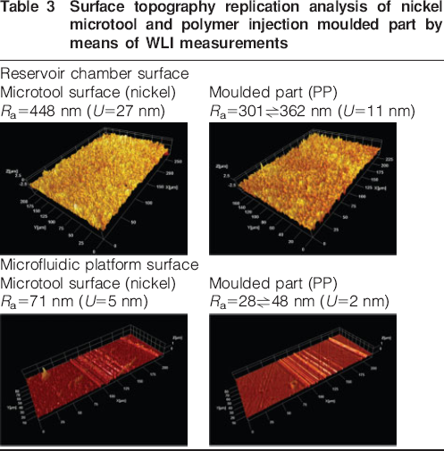
The same calibration procedure was applied to the corresponding tool surface. Measuring results and uncertainties are indicated in Table 3. The comparison with polymer replica and the influence of different injection moulding parameters are discussed in the following sections.
Surface topography replication analysis of nickel microtool and polymer injection moulded part by means of WLI measurements
Measurements on reservoir chamber surface
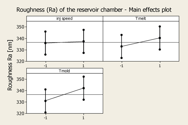
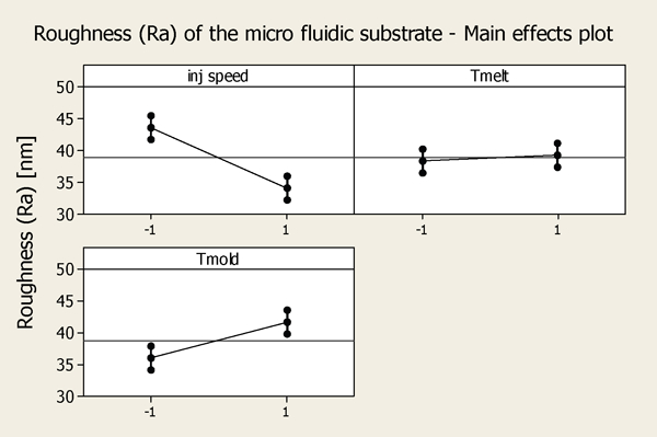
The measurements on the reservoir chamber surface were analysed, and the effect of the different injection moulding parameters on the average surface roughness Ra was determined. The measuring uncertainty was calculated, and an average roughness Ra = 337 nm was measured over the whole DOE. The results are graphically reported in Fig. 12, where it can be noticed that an increase of both mould and melt temperature led to an increased roughness of the polymer surface (i.e. better replication of the tool surface topography). On the other hand, the higher injection speed did not have an effect on the replication quality. The average replication capability calculated as the ratio between the reservoir chamber surface roughness and the corresponding Ra of the tool was 75%: the injection moulding could not provide a full replication of the tool surface texture in the reservoir chamber. The graphs also show the challenge of obtaining a low measuring uncertainty when performing optical surface topography measurement on the polymer surface, especially if compared with the variations produced by the process. In fact, a standard deviation of 11 nm due to the DOE window span was calculated and was in the same range of the measuring uncertainty.
Polymer surface roughness in reservoir chamber (bars represent expanded uncertainties): main effects plot of three investigated process parameters on average surface roughness
Measurements on substrate surface
The measurements on the microfluidic system substrate surface were also analysed by means of the DOE statistical tool. The effect of the different injection moulding parameters on the average surface roughness Ra was calculated, also taking uncertainty into account. As graphically represented in Fig. 13, strong effects can be observed with variations larger than the measuring uncertainty. In particular, a higher temperature of the mould led to a slightly higher surface replication (see the large tilt of the segment in Fig. 13). On the other hand, a higher injection speed caused a decrease in the roughness of the polymer surface (see the negative tilt of the segment). This was probably the result of flow instability due to the higher injection speed that inhibits surface replication of surface features in the nanodimensional scale. Finally, it can be observed that recommended melt temperatures should be employed and not exceeded to avoid polymer degradation.
Polymer surface roughness in microfluidic substrate area (bars represent expanded uncertainties): main effects plot of three investigated process parameters on average surface roughness
The ratio between the microfluidic substrate surface roughness and the corresponding Ra in the tool, ranging from 40 to 67%, clearly indicates the challenge for a conventional injection moulding process to replicate surface features in the nanometre scale, even when a large process window is investigated.
Influence of dimensional range on surface replication
The surface topography measurements on both types of surface have been related to their respective tool surface and subsequently expressed in terms of surface replication factor (as defined in the previous sections) for all the injection moulding conditions. Then, taking advantage of the statistically designed experimental plan, the obtained set of replication factors were affected by both the process conditions and the reference surface roughness in the tool. As shown in Table 3, the microfluidic platform surface had a low level of average roughness with Ra = 71±5 nm (i.e. Ra in the dimensional range of tens of nanometres); alternatively, the reservoir chamber surface had a higher level of average roughness with Ra = 448±27 nm (i.e. Ra in the dimensional range of hundreds of nanometres).
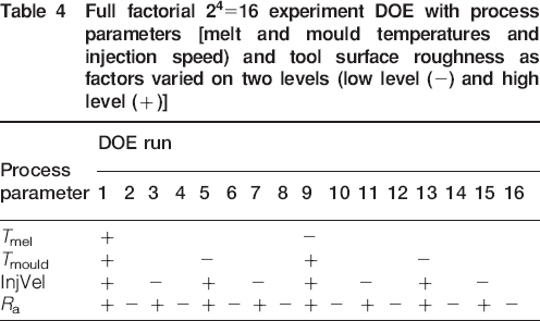
A further statistical analysis has been conducted in order to quantify the effect of the surface roughness dimensional range on the replication factor when compared with the influence of the process parameters. The new DOE resulted in four-factor (melt and mould temperatures, injection speed and Ra of the tool) and two-level (low and high level) full factorial DOEs (Table 4).
Full factorial 24 = 16 experiment DOE with process parameters [melt and mould temperatures and injection speed) and tool surface roughness as factors varied on two levels (low level (−) and high level (+)]
This analysis showed that the surface roughness dimensional range is a much more influencing replication factor than the other process parameters. In particular, with the increase in the surface roughness of approximately one order of magnitude (i.e. from tens to hundreds of nanometres), the replication factor increases (Fig. 14). The measurements showed that injection moulding has a limitation in terms of the replication capability of features below the micrometre scale with a decrease in performance and a decrease in surface roughness even when a large process window is investigated.
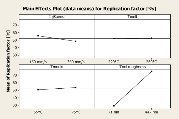
Replication factor main effect plot showing influence of both process parameters and tool surface roughness
Conclusions
Polymer microfluidic chips were injection moulded on a commercially available polypropylene grade. The process windows in terms of injection speed and melt and mould temperatures were investigated. Dimensional and surface measurements were carried out with an optical CMM and a WLI respectively. The dimensional accuracy of the polymer microfluidic systems was validated over the whole experimental conditions. On the other hand, a limitation in terms of replication capability of submicrometre roughness was observed. In particular, with a decrease in the surface roughness tool from Ra≈450 nm to Ra≈70 nm, a decrease in the ratio between the polymer surface roughness and the corresponding Ra in the tool from 75 down to 40% was observed.
The analysis suggests that an adapted compression moulding process with either modified initial filling17 or final filling phase18 should be implemented when shot volume parts in the gram range with submicrometre and even nanometre range features need to be replicated.
Additionally, the traceability and quality of the measurements have been assured by establishing a comprehensive uncertainty budget for all the measurements. The importance of carrying out a DOE analysis with integrated measuring uncertainty was demonstrated in both dimensional and surface measurements. Especially when performing DOEs, uncertainty and dimensional measurements play important roles of being the link between the process effects on the part and the numerical data to be analysed.
Footnotes
Acknowledgements
This paper reports the work undertaken in the context of the project ‘Converging technologies for microsystems manufacturing’ (COTECH). This is a large scale collaborative project supported by the European Commission in the Seventh Framework Programme (grant no. CP-IP 214491-2). The work was also carried out with the support of the 4M Network of Excellence ‘Multimaterial micromanufacture: technology and applications’ (European community founding FP6-500274-1; ![]() ). Tooling, polymer replication and dimensional measurement activities were carried out in connection with the work program of the Processing of Polymer Technology Division (4M Work Package 4) and of the Metrology Division (4M Work Package 5). Surface topography measurement activities were performed within a collaborative research programme carried out between the Section for Micro/Nano and Precision Manufacturing (MPP) at MEK-DTU (Kgs. Lyngby, Denmark), Department of Innovation in Mechanics and Management (Padova, Italy) and CIVEN (Italian high-tech cluster of nanotechnologies applied to materials, Venice, Italy).
). Tooling, polymer replication and dimensional measurement activities were carried out in connection with the work program of the Processing of Polymer Technology Division (4M Work Package 4) and of the Metrology Division (4M Work Package 5). Surface topography measurement activities were performed within a collaborative research programme carried out between the Section for Micro/Nano and Precision Manufacturing (MPP) at MEK-DTU (Kgs. Lyngby, Denmark), Department of Innovation in Mechanics and Management (Padova, Italy) and CIVEN (Italian high-tech cluster of nanotechnologies applied to materials, Venice, Italy).