
Abstract
This paper presents a review of the different electron microscopy techniques for characterisation of weld microstructures with an emphasis on the techniques to determine morphology, composition and structure determination of ferritic weld metal. The focus will be on techniques which provide an advantage due to either ease of use or greater depth of information, thereby supplementing the information obtained by traditional characterisation techniques such as scanning electron microscopy and transmission electron microscopy. The use of electron backscattered diffraction with orientation imaging microscopy as a tool to understand phase transformation paths and ferrite variant selection will be discussed. The use of energy dispersive X‐ray spectrometry and electron energy loss spectrometry as complementary techniques to determine chemical composition of precipitates will be described. The advantages of annular dark field imaging and bright field scanning transmission electron microscopy for imaging precipitates and defects will be discussed.
Introduction
The use of conventional scanning and transmission electron microscopy techniques for characterisation of microstructures and precipitates in metallic systems is well known. This review details the characterisation of weld microstructure using recent advances that use the scanning electron microscope (SEM) or the transmission electron microscope (TEM) as the instruments of choice. Characterisation of weld microstructures has dealt with many distinct areas.1– 16 The following section describes the different microstructural features of interest and introduces the techniques that are used for characterisation.
Prior austenitic grain sizes and their effect on the mode of austenite transformation to ferrite are well established. High strength ferritic weld microstructure is predominantly bainitic and the packet sizes of bainitic sheaves is considered the critical ‘grain size’ for crack propagation and Hall–Petch strengthening. However, apart from optical microscopy based image analysis methods for austenite grain size determination, the use of electron backscattered diffraction (EBSD) based techniques to estimate the effect of alloying additions on austenite grain size and subsequent effects on austenite decomposition have gained popularity.
In the case of continuously cooled bainitic microstructures, very little systematic characterisation work has been performed to evaluate the effect of cooling rate and alloy composition on variant distribution of bainitic laths within each austenitic parent grain. The use of EBSD in conjunction with orientation imaging microscopy (OIM) techniques, and knowledge of the phase transformation mode of austenite, can be used to understand variant selection and their effect on weld properties. A summary of the developments in this area is presented.
Weld metal properties are known to be affected by local brittle zones, of which martensite–austenite–cementite constituents is a subset. However, there has been no easy way of determining the effect of alloying additions on the formation of these local brittle zones or to quantify the amounts of retained austenite and cementite formed in the different regions of the microstructure. The use of a focused ion beam (FIB) to do site‐specific sample preparation for TEM imaging of martensitic regions within small pockets of retained austenite is ideal for this purpose.
The identification of inclusion composition, structure and morphology, and quantification of inclusion size distribution has been studied in different systems. The link between inclusion size distribution on fatigue properties and the effect of hard, brittle inclusions on cleavage crack initiation has prompted research in this field. The effect of inclusions on nucleation of intragranularly nucleated ferrite critical for weld metal toughness has been studied in great depth. The use of scanning transmission electron microscopy (STEM) imaging techniques in tandem with analytical electron microscopy techniques such as energy dispersive spectrometry (EDS) and electron energy loss spectrometry (EELS) to study elemental segregation and characterise inclusion and precipitate content is a powerful technique and examples of the use of these techniques in ferritic weld metal is detailed. In addition, the use of energy filtered transmission electron microscopy (EFTEM) as an imaging technique for studying precipitation in Cr–Mo weld metal is detailed.
Table 1 shows a comprehensive list of characterisation techniques and the applications to resolve the microstructural features relevant to weld metal microstructures.
Summary of electron microscopy based techniques for weld metal characterisation*
*EBSD: electron backscattered diffraction; OIM: orientation imaging microscopy; BF‐TEM: bright filed TEM; DF‐TEM: dark field TEM; SAD: selected area diffraction; FIB: focused ion beam; HAADF: High angle annular dark field; STEM: scanning TEM; CTEM: conventional TEM; EDS: energy dispersive spectrometry; EELS: electron energy loss spectrometry; EFTEM: energy filtered TEM.
Electron backscattered diffraction/orientation imaging microscopy
Electron backscattered diffraction patterns are obtained in the SEM by the interaction of the primary electron beam with the sample surface at a steep inclination to minimise absorption and maximise diffraction. The sample surface needs to be relatively strain free and clean as the interaction of the electron beam with the sample will be restricted to the surface layers (∼10 nm). The diffraction patterns are imaged using a CCD camera and an automated image analysis technique is used to obtain orientation, phase and structure information.
Venables and Harland pioneered this technique in 1973,17 but it is only in the last 20 years that this technique has gained popularity. The reviews by Dingley18 and Humphreys19 detail the developments in this field and document the critical technological advancements. The visualisation of polycrystalline structures using EBSD pattern maps is now a very well established and popular technique.19– 22 There have been several efforts to evaluate different types of steel microstructures ranging from low carbon steel to dual‐phase and transformation induced plasticity (TRIP) steels.22– 27 There have also been recent papers that derive the texture of the parent austenite from the information on the texture of the ferrite grains.
A few case studies of the use of EBSD/OIM to characterise ferritic weld microstructures are described below. All microstructures presented in this review paper were taken with an XL‐30 ESEM fitted with a field emission gun that can operate up to 30 kV providing a 20 Å digital resolution. The microscope is equipped with an EBSD system and phase identification system from TSL.
Prior austenitic grain boundary determination
The prior austenitic grain size determination is critical to understand the mode of phase transformation of austenite to ferrite and the consequent effect on strength and toughness. Most characterisation work on prior austenitic grain size determination utilises a selective etching technique or a heat treatment to delineate the boundaries and measure them using standard stereological techniques. However, with higher strength ferritic steels and welds the austenitic grain boundaries are not delineated clearly enough to accomplish this measurement with accuracy. Electron backscattered diffraction offers a convenient and accurate method of determining the austenitic grain boundary locations even in the absence of retained austenite in the microstructure. In addition, EBSD is also capable of scanning large areas and obtaining statistically significant number of austenite grains (depending on grain size) for this estimation. The details of this technique are explained below.
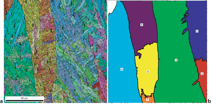
Humbert gey procedure
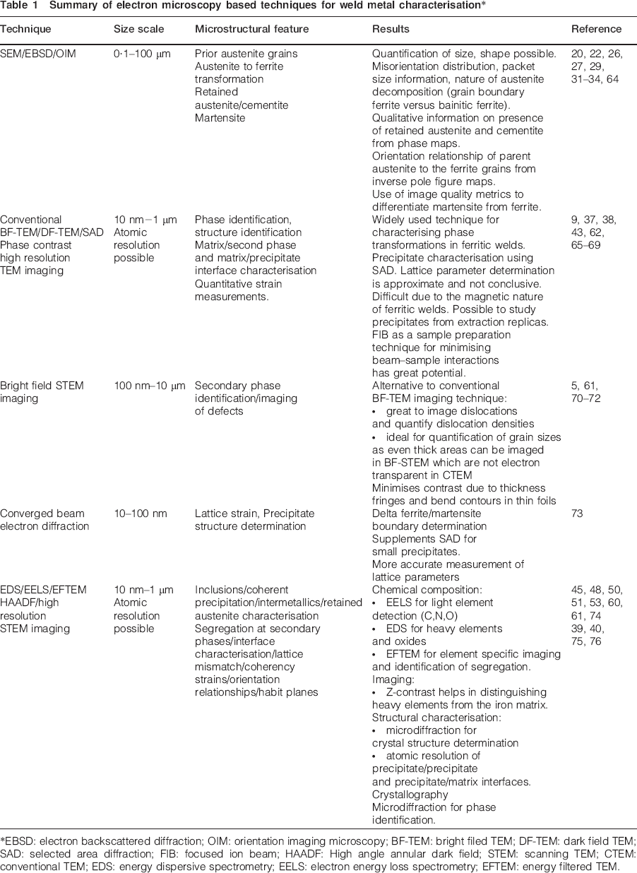
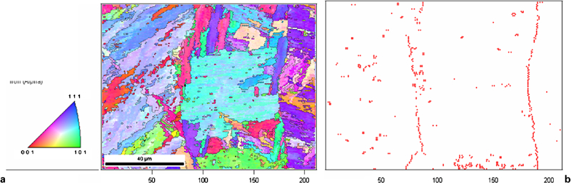
This procedure is described in Ref. 28 for α–β transformations in titanium; however, it can be used for any displacive transformation and is illustrated with a case study. Figure 1a shows an inverse pole figure (IPF) from the as welded region of a high strength ferritic weld with a completely bainitic microstructure. The approximate weld metal composition is Fe–1Al–3Mn–1Ni. This weld deposit was made with an experimental 2·0 mm diameter self‐shielded flux cored arc welding process (FCAW‐S). The ferrite variant distribution is related to its parent austenite and the orientation relationship (OR) is close to the Kurdjumov–Sachs (KS)/Nishiyama–Wassermann (NW) OR. In the case of bainitic and martensitic transformations, it is known that the variants have a distinctive OR with the austenite grain into which they grow. Determining the orientation of the different ferrite grains with respect to a sample reference frame, the misorientation between the neighbouring ferrite grains can be calculated. With prior knowledge of the crystal symmetry and ORs between the austenite and ferrite, the minimum misorientation (disorientation) between neighbouring grains can be calculated. For a given OR, the disorientation of the different variants (24 for KS, 12 for NW) formed off of the same parent austenite is shown in Fig. 2a for both KS and NW ORs. Figure 2b shows the distribution of the misorientation within one austenite grain from Fig. 1. The discrete nature of the orientation distribution aids in distinguishing one austenite grain from another and in determining the orientation of the parent austenite.28, 29 If neighbouring ferrite grains are not related to one another by any of the distinct disorientations specified by the OR, they belong to a different austenite grain. Using this as a constraint, the ferrite/ferrite grain boundaries that are misoriented according to the rules imposed by the OR of the ferrite with its parent austenite can be filtered. The remaining ferrite/ferrite boundaries are plotted to delineate the prior austenitic grain boundaries as shown in Fig. 1b assuming a KS OR. Note that the prior austenite grains are significantly larger than the apparent scale of the transformed microstructure seen in Fig. 1a. Once the prior austenitic grain boundaries have been identified, the variant distribution within a prior austenitic grain can be studied in greater detail.
a IPF showing bainitic microstructure within columnar prior austenitic grains and b misorientation filtered orientation map showing outline of prior austenitic grains: isolated pixels are because of improper indexing
a distribution of varaints according to minimum misorientation for different ORs seen in steels and weld microstructures and b misorientation distribution of variants within prior austenitic grain from a
Austenite to ferrite decomposition
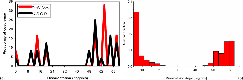
The austenite to ferrite transformation in weld literature has been classified on the basis of visual or morphological differences amongst the different ferrite allotriomorphs.30 This classification is sufficient and very useful in determining the effect of alloying additions for traditional C–Mn and most low alloy weld metal microstructures. However, with the increase in alloying additions to increase strength, the development of welding consumables for Cr–Mo, dual phase, and TRIP steels, this classification system is inadequate in discerning the differences in the weld microstructures. Electron backscattered diffraction /OIM provides a unique methodology to characterise the different ferritic allotriomorphs. The review paper on the use of EBSD to distinguish different ferrite transformation products and the ability to distinguish between acicular ferrite, upper bainite, lower bainite and martensite by Gourgues31 gives excellent detail on the procedure. For example, the different types of ferritic weld microstructures can be discerned by plotting IPFs. The IPF shown in Fig. 1a is a typical bainitic microstructure with carbide free bainite being the dominant microstructural constituent. Figure 3a is an IPF from the as welded region of a weld produced with an Fe–1·0Al–0·2C–0·5Mn composition from an E70T‐7 (AWS 5·20) electrode. This microstructure contains large amounts of grain boundary nucleated allotriomorphic ferrite, widmanstatten ferritic laths.
a IPF of as welded region of weld with mixture of widmanstatten ferrite (WF) and bainite (B), b IPF of as welded region of weld with predominantly carbide free bainite and martensite (M), c IPF of martensitic twins from b showing alternating orientations and d pole figure of martensitic twins from c showing misorientation between two twin orientations
Morito and Furuhara27, 32 have studied the variant selection mechanism in Fe–Ni steels that were isothermally transformed at different temperatures. The variant selection was classified assuming a KS OR. The same methodology can be used to study variant selection for continuously cooled weld microstructures. Figure 3b is obtained from weld metal deposited with an experimental electrode and the self‐shielded flux cored arc weld process, showing a mixture of carbide free bainite and martensite. The choice of twin related variants can be clearly and unambiguously determined using this technique. The variant classification methodology employed by Furuhara is used to label the twin related variants seen in Fig. 3c. Figure 3d shows the pole figure corresponding to the twin related variants. Several research groups have also demonstrated the possibility of self‐accommodation and plastic strain reduction in the austenite during transformation in different types of steels23, 26, 29 using EBSD analysis and these approaches are equally valid for weld metal microstructures.
Cayron33, 34 has shown the ability to reconstruct austenitic grains and to generate automatically the different variants produced within the parent austenitic grains using theoretical groupoid structure formed by the variants and their operators. This reconstruction technique is illustrated in Fig. 4. Figure 4a is an IPF of the as welded region of a ferritic weld whose composition is Fe–1·0Al–0·04C–2Mn. The weld is completely bainitic and no retained austenite could be detected. However, the ARPGE program34 is capable of reconstructing the prior austenitic grains with only the Euler angles and the OR as inputs. In addition to reconstructing the prior austenitic grains, the program is also capable of calculating the different ferrite variants within each parent grain. Details of this technique are provided in the original papers.33– 36
a IPF and image quality map of as welded region of self‐shielded flux cored arc weld showing predominantly bainitic ferrite and b prior austenite grains reconstructed from data from a using ARPGE program developed by Cayron34
Scanning transmission electron microscopy
Conventional transmission electron microscopy (CTEM) combined with selected area diffraction (SAD) has been widely used as a characterisation technique for weld metal and precipitate characterisation.10, 37, 38 However, the STEM provides several important advantages over the CTEM mode. The image in a STEM mode is collected serially by rastering the beam over the sample, the signals received are amplified and digitised before displaying them on the screen. The main difference between STEM and CTEM modes is the use of a converged beam to raster the sample in STEM mode, in comparison to a defocused beam of nearly parallel electrons in the CTEM mode. In a (S)TEM microscope, which is a dual mode instrument that can be operated in both CTEM or STEM modes, the condenser apertures are used to define the convergence angle ‘α’ that is rastered over the specimen. The signals from the sample are scattered over different angles depending on the nature of their interaction. Imaging in STEM mode uses two types of detectors. In ‘bright field’ STEM (BF‐STEM) imaging, the transmitted electron intensity is recorded with a bright field detector that is positioned on the optic axis of the microscope. These images are closest to the imaging conditions in conventional BF‐TEM imaging. The other detector is the annular dark field (ADF) detector which collects the electrons that are scattered 15–150 mrad and gives a dark field STEM (DF‐STEM) image. Using an appropriate condenser aperture to give a large convergence angle and small camera length, it is also possible to use the detector to form a high angle annular dark field (HAADF) image which uses electrons scattered through 50–150 mrad to form an image.39, 40 This imaging technique is quite useful to minimise diffraction contrast and show the atomic number Z dependence due to the scattering dependence on Z. This makes HAADF imaging ideal for imaging precipitates that are coherent with the matrix, but are chemically different from the matrix, while minimising the obscuring effects of the strong strain contrast for the highly dislocated grains that are quite common in weld microstructures.
Bright field STEM is ideal for characterising the structure and morphology of the complex precipitates, inclusions and microphases that occur in ferritic weld metal. This imaging technique is also quite useful for imaging thicker regions of the foil and expands the useful portion of the samples prepared by traditional sample preparation techniques such as ion milling or electropolishing. Figure 5 shows a BF‐STEM image of a packet of retained austenite and twinned martensite within the as welded region of a weld metal designed to mimic the composition of TRIP steels.41
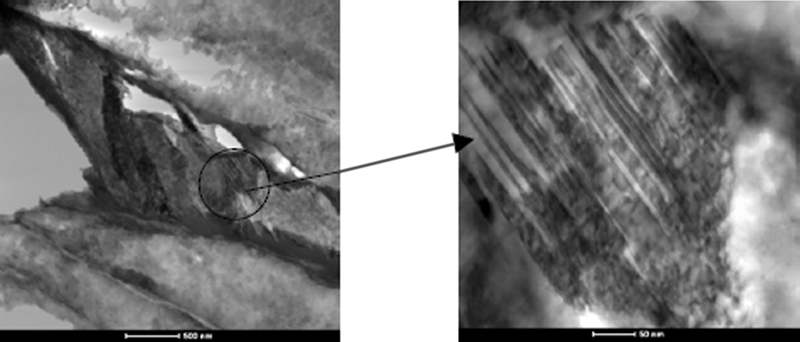
Image of BF‐STEM showing pocket of retained austenite with twinned martensite within retained austenite region from Ref. 41
The following section provides an example of the characterisation of inclusions/precipitates and minor phases. Such as small packets of martensite/austenite in ferritic weld metals, using STEM in conjunction with EDS, EELS and EFTEM.
Inclusion characterisation using EDS/EELS
Open arc welding processes utilise different methods to protect the deposit from oxygen and nitrogen contamination. Depending on the arc welding process, multiple sources can be responsible for the inclusion content of the weld. In addition to the oxygen and nitrogen introduced intentionally through oxides added in the flux, oxygen can also originate from the shielding gas or oxygen pick‐up from the atmosphere as well as slag generated by the intentionally added fluxing additives.
The inclusions that form in the molten weld pool get trapped during solidification in the interdendritic regions. In addition, there may be additional carbides and nitrides that precipitate during solid state transformation of the weld metal. By accurate measurements of inclusion size distribution and employing realistic modelling of the inclusion nucleation and growth, it is possible to determine the critical size of inclusions that control mechanical properties.
Over the past 50 years, the transmission electron microscope has become a critical tool for characterisation of defects and quantitative/qualitative measurement of second phase precipitates.42 The development of EDS detectors for the S(TEM) has made mapping of the chemical composition of phases and precipitates possible. Quintana43 characterised the inclusions formed in an open arc weld deposit with two different aluminium contents. They showed that the formation of inclusions in these welds is a complex process dependent on composition of the different deoxidisers and denitriders in the system. They showed that the aluminium rich weld had predominantly aluminium nitride inclusions while the low aluminium weld had an aluminium oxide with titanium nitride skin growing on the oxide. They also showed some evidence of aluminium oxide particles on titanium nitrides cuboidal inclusions (Fig. 6). They used EDS to estimate chemical compositions of these inclusions. Spanos44 used EDS on a gas shielded weld deposited with an ultra low carbon welding consumable to map the different elements present in the dominant inclusions. There have been very few efforts to characterise the crystal structure and the chemical composition of complex inclusions beyond qualitative EDS analysis and simple diffraction work to supplement the chemical analysis. The presence of light elements such as carbon and nitrogen in the inclusions makes quantitative assessment difficult. Electron energy loss spectrometry is an ideal technique for characterising light elements such as carbides/nitrides in steels. A 0·01%C minimum detectable limit was determined by Menon45 using a LaB6 electron emitter and a parallel EELS spectrometer. Walters46 did detailed analysis of non‐metallic inclusions in C–Mn weld metal using EELS/TEM analysis and suggested possible morphologies and chemical compositions. Scott47 used extraction replicas to lift out the precipitates from the matrix to quantify carbon and nitrogen. The interesting feature in their extraction technique is the use of RF sputtered amorphous alumina. The RF sputtered alumina has the advantage that it provides a rigid support for the precipitates and does not undergo charging in the electron beam. They used this technique to analyse carbonitrides of titanium. He and Baker48 also used parallel EELS to quantify the nitrogen content in Zr(C,N). The lattice parameter of the precipitates was determined from SAD measurements.
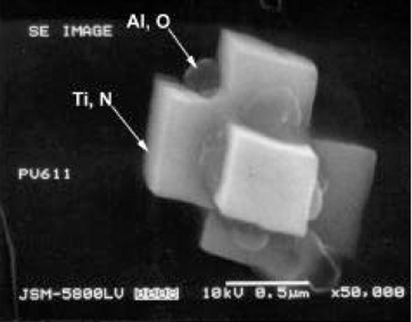
Complex inclusion seen in ferritic welds showing titanium nitride with aluminium oxide skin from Ref. 43
The case study described below is an inclusion characterisation of a weld deposited with an open arc welding process.5 The inclusions were characterised, firstly in the matrix using electropolished samples, and then further analysed after extracting them onto carbon films. The characterisation was performed using a Tecnai TF‐20 microscope. The DF‐STEM images of the as welded region show that the precipitates have a facetted structure with a distinctive core/shell configuration (Fig. 7a). EDS line scans across the precipitates in this weld indicate a transition in composition from an aluminium/magnesium rich core to a titanium/zirconium rich shell. Figure 7b shows a typical line profile across one of these complex precipitates. The aluminium and magnesium composition traces show increases over the core of the precipitate, and drops down to baseline levels in the shell region. Titanium and zirconium composition traces are much higher in the shell region and drop in the core region. The oxygen line profile also has a peak at the core region of the precipitate. These results indicate that the core of these precipitates is a complex oxide of aluminium and magnesium. The low magnification DF‐STEM image of the precipitate (Fig. 7a) provides an indication of the distinctive interface morphology of the core and shell regions. In addition to the EDS analysis of the precipitates, EELS was used to establish the presence of nitrogen, oxygen and carbon in the core/shell region of the precipitate due to its ability to detect light elements and better spatial resolution. Selected inclusions that were overhanging from an edge or a hole in electropolished samples were used for characterisation to minimise the signals from the matrix. A 1 nm wide electron probe in the STEM mode was used to image the area and the EELS spectra obtained were compared to standard energy loss peaks49 and identified accordingly. Figures 8a shows EELS spectra taken from the shell region of the precipitate, consistent with the shell region is a titanium/zirconium nitride (as confirmed with electron diffraction). There is no indication of oxygen in the shell region. An arrow indicates the position of the oxygen edge in the EELS spectrum. Figure 8b shows an EELS spectrum from the core region of a similar precipitate where the core region is through the thickness of the foil and shows the presence of oxygen, in agreement with the EDS oxygen profiles obtained from similar precipitates.
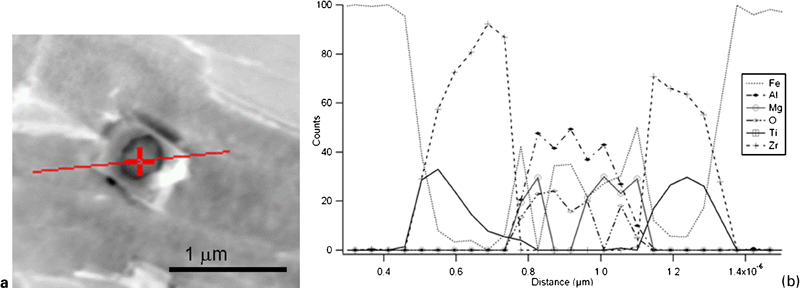
a core–shell precipitate from weld with titanium and zirconium and b EDS line scan analysis from core and shell regions showing Al and Mg rich core and Ti/Zr rich shell from Ref. 5
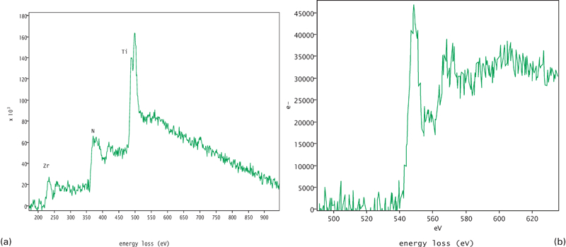
Analysis by EELS from a shell region showing Zr, Ti and N [note absence of oxygen edge (arrow)] and b core region from similar precipitate where core shows presence of oxygen5
Precipitate characterisation using EFTEM
High temperature creep properties and cracking susceptibility of Cr–Mo steels and weld metal have been shown to be controlled by the type of carbides/carbonitrides formed in the weld and the heat affected zone. This has been the focus of many investigations that involve EFTEM. This technique utilises inelastically scattered electrons (similar to EELS) and an energy filter to selectively use certain energy windows to produce element specific images that are visually similar to EDS elemental maps. References 50–54 provide the details of the technique. The work of Courtois55 on niobium carbonitrides in steels details the quantification of precipitate sizes as well as compositions. In their work, Fe–M2,3 and Nb–N2,3 edges were used for imaging. The three window method is used for generating the niobium elemental map with the main window centred on the niobium edge and two pre‐edge windows (3 eV in width) are used to extrapolate the background around the edge. The area fraction of the precipitates was then determined from the elemental images and converted into volume fractions by measuring the thickness of the foil using EELS. Similar work has been carried out on nitrides of vanadium, Laves phases and Cu precipitates in steels by Hattestrand and Andren56 using jump ratio images50 of V, Nb, Cr, W and Cu. Sarosi57 demonstrated the use of EFTEM for quantifying γ′ precipitate size in nickel based superalloys, and also used a novel technique to measure thickness to quantify the volume fraction of the precipitates.
Atomic scale resolution of precipitates using HAADF imaging
As mentioned above, HAADF (or Z contrast) imaging in the STEM is achieved by rastering a coherent fine probe over the sample and collecting high angle scattered electrons (50–150 mrad) using an ADF detector to form an image whose intensity is a convolution of the microscope's point spread function and an object function. The microscope's point spread function is the illuminating probe intensity spread while the object function is an intensity distribution with local peaks at atomic columns. This mode uses highly scattered electrons and is an incoherent imaging technique that has certain advantages over high resolution TEM mode. The high resolution TEM mode is a phase contrast imaging technique which involves interpretation of images as the image contrast is modified by defocus, spherical aberration and sample thickness. However, the HAADF imaging mode results in a directly interpretable image with the contrast dependent mainly on the atomic number (Z1·5 to Z1·7 dependence) of the columns over which the probe resides, and shows no contrast reversal over a wide range of sample thicknesses. Some examples of HAADF imaging used in conjunction with EELS and EFTEM for imaging precipitates are referenced.5, 54, 58– 60 An example of what is possible with HAADF imaging in conjunction with DF‐STEM imaging for crystal structure identification of complex inclusions is shown in Fig. 9 from Ref. 5. The Z contrast image is from the shell region of a core–shell (Zr,Ti)N precipitate in the [001] zone. The corresponding DF‐STEM image is shown alongside indicating the prominent growth facets. The insets show the corresponding SAD pattern and the atom positions corresponding to the intense bright spots in the image. In this orientation, the Ti/Zr atoms and the nitrogen atoms share the atomic columns with the Ti/Zr atoms contributing to the intensity of the image. The uniformity of contrast suggests that both Ti and Zr are randomly distributed with no preferential formation of either nitride. This real time identification of atomic columns can be used to position the probe for atomic scale EELS spectroscopy and has been utilised in the analysis of other candidate oxide systems.61 Though this technique has not yet been used extensively in characterisation of weld microstructures, there is plenty of scope for using this technique to achieve fundamental understanding of heterogeneous nucleation sites and nanoscale precipitation in ferritic weld metal.
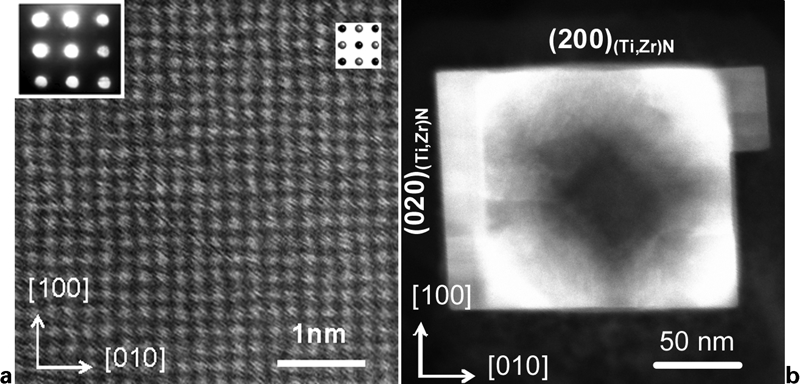
a Z contrast STEM images along [001] orientation [bright intensity shows positions of Ti or Zr atoms in lattice; structure is also indicated (black: Ti, Zr; grey: N); insets shows SAD patterns along respective zone axis] and b DF‐STEM image of core–shell precipitate along [001] zone axis
Sample preparation
Traditional sample preparation for TEM involves thinning samples mechanically followed by either punching out or cutting out a 3·0 mm disc, then electropolishing using a suitable etchant. This technique is still ideal for looking at representative areas and to carry out initial exploratory research. However, any review on recent advances in microscopy techniques for weld microstructure characterisation is incomplete without referring to the FIB technique for site specific specimen preparation. As the name suggests, this technique uses an ion beam to mill the sample to electron transparency. There are different methods to prepare TEM samples using the FIB. The most common method is the ‘H‐bar’ method where a sample is mechanically polished, mounted on a grid and then milled from both sides in the FIB. The second is the ‘lift‐out’ method, where the sample is directly extracted from the area of interest by creating a trench with the ion beam and then cut out of the whole object, transferred onto a carbon coated grid using a micromanipulator under an optical microscope. This method is very site specific and less destructive. The third process is using the ‘in situ lift‐out’ method,62 in which a micromanipulator (e.g. the Omni‐probe) is fitted within the FIB chamber enabling specimens to be extracted directly from the surface of the object. This method is ideal for minimising damage, and allows further milling to thin the sample either inside the FIB or subsequently using a low energy ion mill. This also eliminates the need to use a carbon coated grid that will complicate the characterisation of carbide precipitates. An additional, very important advantage of the ‘in situ lift‐out’ technique for magnetic samples like ferritic steels is that it minimises the mass of the sample introduced into the electron column, thus making possible high resolution work on microstructures that are both magnetic and highly strained. This approach is ideal for characterisation of hard spots in welds which have been ascribed to be a mixture of martensite–austenite–cementite. One such example is shown in Fig. 10 where a FIB foil is imaged using BF‐STEM, and ultra fine martensitic twins can be readily observed. A facetted nitride precipitate can also be seen within the grain. These samples are ideal for EELS analysis as the samples can be thinned multiple times and cleaned with low energy ion milling. In addition to the use of FIB for TEM sample preparation, serial sectioning within the FIB in conjunction with SEM imaging can give great detail of the morphology of complex bainitic microstructures in addition to providing insight into the phase transformation paths. The use of the FIB to examine coalesced bainite by Keehan63 in ferritic weld deposits is an excellent example of such a study.
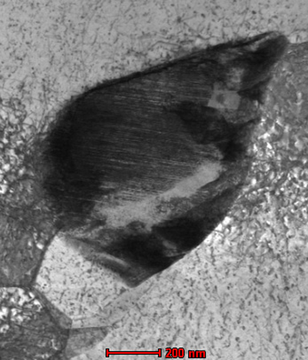
Image (BF‐STEM) from FIB foil showing very fine martensitic twins: facetted core–shell precipitate can also be seen within martensite–austenite region
Summary
This review has attempted to cover some of the electron optical techniques that have not yet gained wide spread popularity in the welding community to the same extent as in other material research areas. While there has been extensive work carried out on characterisation of weld microstructures using conventional analytical electron microscopy, the use of EBSD/OIM and FIB/STEM/EELS/EFTEM is under utilised. The work performed by Hofer and co‐workers on using EFTEM to characterise precipitate evolution in Cr–Mo steels50 and that of Furuhara and co‐workers on using EBSD/OIM to characterise lath martensitic microstructures,27 can also be adopted for in depth analysis of weld microstructures. The development of crystallographic analysis tools similar to that developed recently by Cayron33 maximises the information that can be extracted from the data collected through EBSD and provides new insights into the effect of welding procedures, alloy content on grain size distribution, and phase transformation in ferritic/martensitic welds. The use of BF‐STEM imaging is ideal for examining electropolished samples as it maximises the area available for characterisation and minimises the effect of strain and thickness in comparison with CTEM techniques. Imaging using HAADF STEM can provide great detail about the morphology and crystal structure of inclusions that form during solidification. This technique in tandem with EELS has the ability to provide atomic scale information about the structure and chemical composition of these complex inclusions. The FIB provides a method to perform site specific work on fracture surfaces and high resolution electron microscopy on magnetic samples by minimising sample mass, thus decreasing the interaction between the sample and electron column. These advanced characterisation methods provide revolutionary new capabilities for understanding microstructure development and performance of welded materials.
Footnotes
Acknowledgements
The authors acknowledge The Lincoln Electric Company, for their support.