
Abstract
Electron microscopy has been an important technique for the advancement of materials and joining science allowing studies from the macro‐ to the atomic scale. Such studies are normally performed ex situ, i.e. the material is analysed before and after it has been submitted to an external condition such as welding, deformation and/or heat treatment. Nevertheless, researchers have always looked for experimental approaches to study dynamic processes in real time, i.e. in situ. In the last few decades, advances in electron microscopy have made possible the implementation of in situ experiments that mimic production and service conditions within both transmission electron microscopes (TEM) and scanning electron microscopes (SEM), depending on the scale, material and phenomenon of interest. In the study presented here, the advantages and challenges associated with in situ SEM experiments are discussed with particular focus on structural materials. An introduction to SEM and in situ experiments, their features, limitations, challenges, and the associated instrumentation is given, followed by a review of relevant research work in this field.
Introduction
Starting with the development of the electron optics theory by Busch (1926), passing through Ernest Ruska's transmission electron microscope (TEM) implementation (1931), continuing with Manfred von Ardenne pioneering work on the scanning electron microscope (SEM) (1938), and finally V. K. Zworykin's SEM prototype (1942), which anteceded the launch and series production of SEMs leaded by Charles Oatley at Cambridge Scientific Instruments (1965). Since then, electron microscopy has been widely used as a fundamental technique to obtain valuable information about the inner structure of matter.1– 3
Electron microscopists recognised early on that many challenges in materials science, some of them related to phase transformation and failure mechanisms, required experiments involving real time observation of the studied material subjected to specific conditions, such as atmospheric pressure, temperature, electrical or magnetic fields, and load, among others. This led to the rise of in situ electron microscopy experimentation in the 1960s.4 In situ is defined as where a particular phenomenon is observed and studied in real time. However, the characteristics of the electron microscope limit the conditions and phenomena that can be studied in situ.5
The development of in situ electron microscopy has been pushed forward by TEM technology,6 revealed by the higher number of in situ TEM publications compared to SEM.7 However, the new generation of SEMs shows innovative hardware and software solutions that result in improved performance. This progress has turned the SEM into an extraordinary tool to develop more complex and realistic in situ experiments, achieving even subnanometre scale. The number of scientists dedicated to this field is still small because of the misconception that the development and use of such instrumentation is costly and extremely complex, regardless of the high scientific potential of this technique. At present is situ experiments can be used to address aspects such as phase transformations, cracking, and failure phenomena associated to welding thermal history or thermomechanical service conditions; short term diffusion in dissimilar joints; and even materials solidification. In the near future, new SEM imaging, vacuum, nanomanipulation, and nanofabrication technologies will make it possible to replicate conditions as the ones associated to structural and functional materials joining. Therefore, this paper aims to encourage more researchers, especially within the materials welding and joining community, to engage in the development and use of in situ SEM experiments to overcome fundamental and technological challenges related to the joining of conventional and advanced materials.
In the study presented here, a brief review on scanning electron microscopy and its application to in situ material studies is given, providing a brief overview of the features, advantages, limitations, challenges and potential of such techniques for the understanding of material fundamentals and the development of new materials and joining technologies. Recent advances in SEM in situ instrumentation used for heating and/or straining experiments are also presented. Finally, selected SEM in situ experiments, which use mechanical and thermomechanical testing devices in combination with advanced imaging (special detectors), analysis techniques [X‐ray energy dispersive spectroscopy (XEDS) and electron backscatter diffraction (EBSD)] and/or instrumentation (focused ion beam, FIB), are given to elucidate specific structural material questions.
In situ scanning electron microscopy technology and challenges
Overview of scanning electron microscopy
Scanning electron microscopy is a technique that allows hard and soft, structural, functional and biological materials to be studied at the micro‐ and nanoscale8 by scanning a low to medium energy focused electron beam over the sample surface. The primary electrons are generated in a thermionic, Schottky, or field emission source and accelerated from ∼0·1 up to 40 keV, and finally scanned across the sample's surface by deflection coils.9 The image produced is based on the interaction between the electron beam and the sample. As a result of this interaction, different types of signals are generated from each point of the sample among these signals; the most commonly used are the secondary electrons (SE), the backscattered electrons (BSE), the backscattered diffracted electrons (EBSD) and the characteristic X‐rays.10, 11
The image modes are based on these different signals, which require specific instrumentation to collect and process them. For SE imaging, a combination of a scintillator and a photomultiplier, know as Everhart–Thornley (E–T) detector, is used, which takes advantage of the secondary electrons low energy to deflect them towards a collection grid. In the case of BSE, their high energy prevents the electron deflection towards the detector. Therefore, a solid state detector, a P–N junction diode, is located above the sample, near the pole piece of the last lens of the microscope. In order to allow the continuous electron source operation and to reduce scattering for both, the primary electrons during flight from the source to the sample and the electrons generated or scattered at the specimen as they travel to the detectors, the microscope internal pressure is normally kept at very low levels (vacuum). Table 1 shows the resolution of different image modes and the vacuum level to several types of SEM's.
Characteristic spatial and energy resolution, and vacuum level in conventional (C‐SEM), low vacuum (LV‐SEM) and environmental (ESEM) scanning electron microscopies
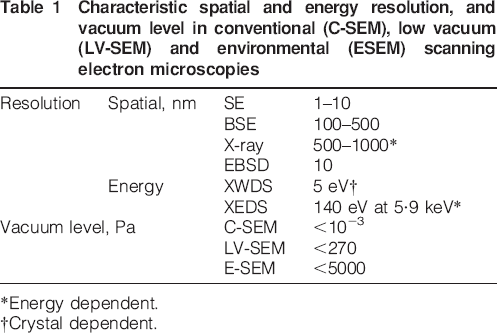
*Energy dependent.
†Crystal dependent.
Challenges associated with in situ SEM testing
The phenomena that can be studied in situ within the SEM are fundamentally limited by the associated instrumentation, specially the SEM, and the intrinsic characteristics of the studied phenomenon, such as required time, spatial and/or energy resolution.12, 13 Several limitations inherent to the SEM structure and function are related to the vacuum environment, which reduces spurious electron scattering by gas molecules and acts as an electrical and thermal insulator. It precludes the analysis of hydrated organic samples and the development of studies involving liquids. The thermal insulating property of vacuum reduces the risk of damaging the microscope components during heating experiments. However, this also makes heating and cooling the sample and measuring its temperature more challenging.14 Nevertheless, the vacuum prevents both sample and instrumentation oxidation during high temperature experiments.
The presence of several sensitive devices (detectors, high precision stage, etc.) tightly positioned around the sample results in space constraints inside the SEM. Some of the components of the microscope use low noise earthed or floating electronics than can interfere with the in situ experiment instrumentation causing spurious signals or even preventing the correct functioning of the SEM.15 In addition, primary beam electrons, BSE, and SE may be deflected by spurious magnetic and electrical fields, arising from the instruments used for the in situ experiment,16 thus compromising the SEM resolution and the image signal to noise ratio (SNR).17 Such SNR is highly dependent on the amount of primary electrons hitting the sample at each specific position corresponding to an image pixel. This amount of electrons is controlled by the electron gun, the SEM optics and the beam scanning rate. Therefore, an image can usually be improved by decreasing the scanning rate, although this exacerbates problems related to mechanical and electronic stability. As in situ experiments address dynamic phenomena, time resolution is very important. Therefore, a compromise should be established between image quality and time resolution. SEMs may provide images from 30 frames/s up to ∼1 frame/min, precluding the study of fast processes.18
The challenges associated with high temperature experiments include: sample drift due to the thermal expansion of the specimen and stages,4, 14, 19 drastic reduction of SNR in SE images obtained from samples kept above 900°C due to thermionic electron emission20 and gas evolution from the sample.
Specimen size and geometry are key factors for in situ mechanical behaviour and failure mechanisms experiments because these factors control the possibility to observe the intended phenomena and the results scalability from the micro‐ or nanoscale to the macroscale.13, 19, 21– 23
In situ SEM instrumentation
In situ SEM experiments can be divided into two major categories: mechanical and other phenomena. The former category covers mechanical phenomena such as deformation, fracture and such like. The second category can be grouped into experiments involving phenomena such as phase transformations, corrosion, etc.5, 13 However, overlap between these two categories is not uncommon and the different experiments require quite differentiated and specific instrumentation.
Several special set‐ups have been designed and built to perform in situ SEM experiments.24– 28 Figure 1 shows some devices for in situ SEM mechanical and thermomechanical testing. A conventional hydraulic mechanical testing system within a large vacuum chamber hosting a horizontal SEM column is presented in Fig. 1a.15 This unique large scale set‐up provides outstanding possibilities to perform mechanical in situ SEM tests on real size specimens. Other devices suitable for conventional SEMs, such as the ones shown in Fig. 1b and c, are used to reproduce mechanical or thermomechanical solicitations and to study bulk materials behaviour under quasi‐static or dynamic stress conditions.29, 30 The high temperature deformation set‐ups make possible studies involving recrystallisation, cracking and failure mechanism at a wide range of temperatures, phase transformations induced by thermal and mechanical energy, and corrosion in different atmospheres. Recently in situ SEM instrumentation for mechanical behaviour studies have been built using microelectromechanical system (MEMS) technology, allowing the application and measurements of low load and strain in small volume of material.31– 33
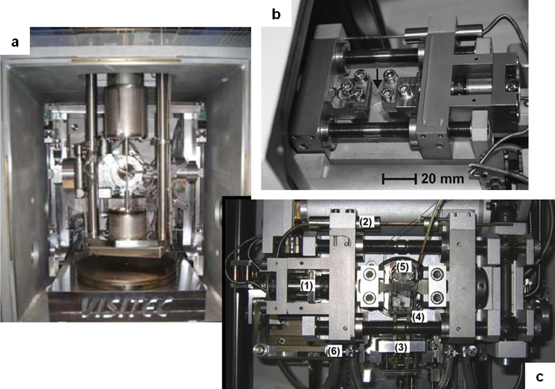
Devices for in situ SEM mechanical testing at different scales
Advances in SEM design and image systems have driven the expansion of in situ SEM studies in recent years.34 Outstanding improvements to electron guns, optics and detectors have resulted in spatial resolutions below 1·0 nm achieved,35 and improved SE, BSE, XEDS36, 37 and EBSD38, 39 imaging. For example, the number of acquired and indexed EBSD patterns per second has been growing at a very high rate, exceeding 300 indexed pixels per second without compromising the orientation data quality.40, 41
The introduction of large area silicon drift detectors (SDDs) for SEM microanalysis has made it possible to obtain qualitative and quantitative XEDS maps in few minutes.42 There are now available 80 mm2 SDDs that can handle 200·000 cps, providing 129 eV resolution (Mn Kα). These EBSD and XEDS technology improvements have mostly been driven by conventional SEM. However, they open great opportunities for dynamic in situ studies in materials joining science.
Nevertheless, the development of specific detectors has been necessary to make in situ studies involving severe conditions possible, such as high pressure (up to 2600 Pa) and temperature (up to 1500°C). Among the most commonly used commercial detectors to deal with these extreme conditions are: SE detector for high pressures, which works as a gas proportional counter;43 high temperature BSE (HT‐BSE) detector, which is immune to thermal electrons and photons emitted by hot samples;44 high temperature SE (HT‐SE) detector, which uses the gas proportional counter principle, applies bias voltages to the sample holder, heat shielding assembly, and final pressure limiting aperture to amplify the signal and suppress the thermal electrons effect.43, 45 However, HT‐BSE detectors have limited spatial resolution and efficiency and produce poor quality images. The commercially available HT‐SE detector is only effective in an environmental SEM (ESEM), precluding its use with conventional high vacuum SEM or even low vacuum SEM (LV‐SEM). Therefore, a high vacuum HT‐SE detector based in post‐detection signal processing has been developed, which is different from the previously used thermal electrons separation before detection.46 This high vacuum HT‐SE detector uses a conventional E–T detector, a high frequency primary beam blanker and signal processing hardware. Figure 2 shows SEM images obtained using conventional SE E‐T, HT‐BSE, and HT‐SE detectors, revealing the improved performance of the HT‐SE detector when compared with the HT‐BSE detector.47
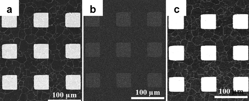
Gold patterns on stainless steel 316L substrate obtained with a conventional E–T SE detector, b HT‐BSE detector and c HT‐SE detector47
Two milestones in SEM evolution have had a significant impact on in situ experimentation. The first was the ESEM and LV‐SEM in the early 1980s,48, 49 the second was the addition of a FIB column to the SEM, resulting in the dual beam scanning microscope (DB‐SM). The ESEM and LV‐SEM allow implementation of in situ experiments involving different gas atmospheres.50, 51 The FIB and DB‐SM revolutionised TEM specimen preparation and the microfabrication technology by the use of material milling and deposition capabilities.52– 55 Nowadays, the DB‐SM powerful milling capability is widely used for the preparation of micrometer in situ mechanical test specimens from specific regions or phases (Fig. 3).13 Micro‐ and nanoindentation and manipulation systems are being adapted to SEM, making a wide variety of original in situ studies possible.56
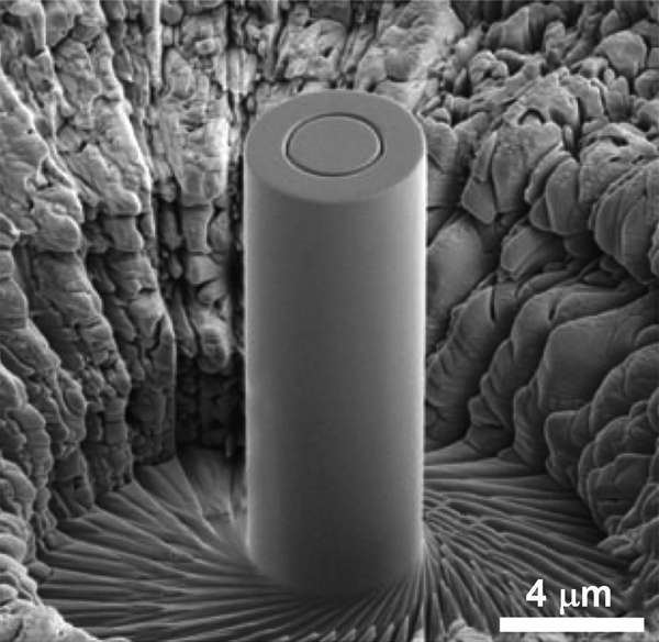
Single crystalline Ni microcompression specimen of 5 μm diameter machined by FIB13
Examples of in situ scanning electron microscopy studies in materials science
Many in situ SEM experiments have been successfully performed in the last years. The most common and successful ones involving structural materials deal with mechanical and failure behaviour at different temperatures, phase transformations induced by mechanical and thermal energy, and corrosion under different atmospheres and temperature conditions.18
Mechanical or thermomechanical in situ experiments
Mechanical, thermomechanical and heating are among the more relevant experiments to the welding and joining community because of the possibility to study phase transformations, stress/strain effects, residual stresses evolution, cracking and failure mechanism associated with the joining process or undergone by welded joints. Study of the mechanical behaviour of materials was one of the first in situ electron microscopy applications.4 Frequently, in situ mechanical experiments mimic some macroscopic mechanical test features as sample geometry and strain/stress rate. Such macroscopic mechanical tests are normally performed under standard conditions,57 allowing results to be compared. Nevertheless, size effect is an important factor that precludes correlation between macroscopic and microscopic mechanical test results. Thus, most SEM in situ mechanical experiments are considered very important tools to perform phenomenological studies, but are not yet an alternative to engineering properties quantification. However, when the micro‐ and nanoscale properties are the focus of the investigation, such in situ tests may provide both phenomenological and quantitative properties information. Such in situ mechanical tests allow the study of deformation processes31, 58 through the direct observation of the involved fundamental mechanism (deformation bands and twins). It is also possible to study the activation of slip systems and the interaction between them and other deformation mechanisms. Failure mechanisms can also be addressed through the observation of crack nucleation and propagation,32, 59 including fatigue crack behaviour.30, 60– 62 An example of the potential of these SEM in situ studies to fully understand and quantify materials mechanical behaviour and its relationship with the micro‐ and nanostructure is the study of the debonding between manganese sulphide (MnS) inclusions and the surrounding steel matrix, which was investigated by in situ SEM tensile testing at room temperature.63 Tests were carried out for two different orientations of the inclusions with respect to the loading axis, longitudinal (L) and short transverse (S). The in situ observation showed that the bond between the MnS inclusions and the matrix was particularly weak in the S direction, with the sulphides delaminating from the matrix at very low applied stresses. On the other hand, when the external load was applied in the L direction, the MnS inclusion interface fractured at high stress levels, even close to the yield stress. Figure 4 shows an in situ SEM test sequence with the external load applied in the S direction, where the interface debonding is evident.
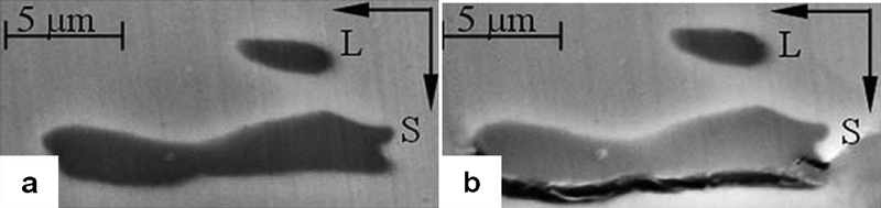
In situ SEM study of MnS inclusions debonding from steel matrix: external load in S direction resulting in applied stress of a 20 MPa and b 1586 MPa63
Another study evaluated the crack propagation rate under thermomechanical cycling for Ni‐base alloy 718 by the use of in situ ESEM experiments.64 Figure 5 shows the crack growth after 80 cycles where the applied temperature ranged from 300 to 550°C and from 300 to 630°C for times of 55 and 75 s respectively. It was found that the temperature at which maximum mechanical load was applied was decisive for both the crack propagation rate and the fracture surface morphology, regardless of whether the temperature was cycled or kept constant. The study indicated that isothermal fatigue propagation data can be used to predict crack propagation rates provided that the isothermal data are taken from the temperature at which the mechanical load peaks are known. There are similar experiments reported elsewhere in the literature.30, 65
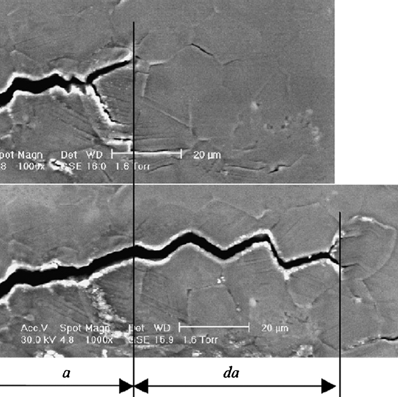
Crack propagation rates under thermomechanical cycling of Ni base alloy 718: measured projected crack growth da = 57 μm for dN = 80 cycles64
In order to understand the fundamentals of the solid state cracking phenomena, ductility dip cracking (DDC), which plagues thick plate welding of Ni base alloy 690,66– 68 an in situ SEM high temperature deformation experiment was developed.12, 47 Autogenous ERNiCrFe‐7 and ERNiCr‐3 weld metal, corresponding to alloys 690 and 600 respectively, were evaluated at temperatures ranging between 700 and 1000°C. The microstrain/stress state was addressed and quantified using digital image correlation (DIC) methodology.12, 24, 69– 72 The DDC susceptibility (threshold strain ϵmin) for both alloys was quantified and compared with macroscale test based on Gleeble thermomechanical simulation, as shown in Fig. 6. The values of ϵmin for alloys ERNiCrFe‐7 and ERNiCr‐3 were 7·5 and 16·5% respectively, confirming the better resistance of ERNiCr‐3 to DDC, as was previously indicated by the strain to fracture (STF) Gleeble based test.73 In addition to the ϵmin quantification, the grain boundary sliding (GBS) and intergranular primary precipitates role on the DDC mechanism were investigated using images obtained during in situ SEM high temperature deformation.
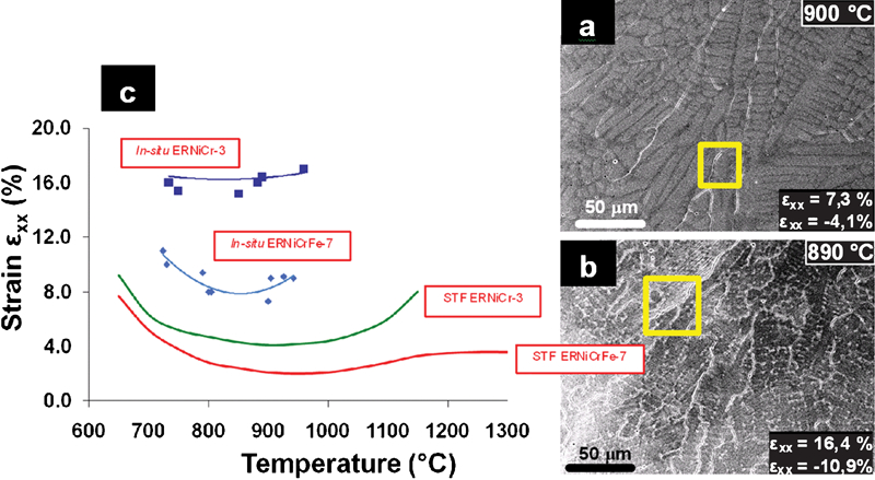
In situ SEM high temperature deformation of Ni base alloys 690 (ERNiCrFe‐7) and 600 (ERNiCr‐3) to study ductility dip cracking phenomena. Snapshots of crack initiation in a) ERNiCrFe‐7 alloy at 900°C and b) ERNiCr‐3 alloy at 890°C. c In situ and strain to fracture (STF) ductility dip cracking susceptibility curves for ERNiCrFe‐7 and ERNiCr‐3 Ni based alloys.12 STF results adapted from Ref. 73
Alloys ERNiCrFe‐7 and ERNiCr‐3 have a differentiated grain boundary (GB) morphology, presenting predominantly flat and undulated GBs, respectively.66, 67 Such GB morphology has an important effect on GBS and therefore, on the DDC resistance. Figure 7 shows two different GBs on alloys ERNiCrFe‐7 and ERNiCr‐3 before and after the in situ SEM high temperature deformation test. The superimposed quadrilaterals allow quantification of two separated GBS components called pure sliding Sp and deformation sliding Sd.12, 47 Table 2 shows the measured Sp and Sd values for the GBs presented in Fig. 7. Direct observation of the deformation process allows errors induced on the GBS quantification by free surfaces displacement after microvoid or microcrack nucleation and propagation to be avoided. As Table 2 shows, favourably oriented and flat GBs on ERNiCrFe‐7 alloy exhibit larger Sd and Sp values than the undulated GBs on ERNiCr‐3 alloy. Such different GBS behaviour is mainly due to the grain boundary topography. GBS is favoured along flat GBs, as the one presented in Fig. 7a and b, promoting strain accumulation at triple points and intergranular second phases. Therefore, direct observation of this high temperature deformation phenomenon has made it possible to establish a direct link between such as welded microstructures characteristics, the GBS phenomena and the consequent limited ductility of ERNiCrFe‐7 alloy in the temperature range between 700 and 1000°C.
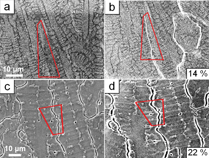
Grains boundaries on alloys ERNiCrFe‐7 (a, b) and ERNiCr‐3 (c, d) during in situ SEM high temperature deformation tests performed at 912 and 927°C respectively. a and c show unstrained microstructures, while b and d correspond to average horizontal imposed strain ϵxx of 14 and 22% respectively. Superimposed quadrilaterals allow quantification of pure Sp and deformation Sd grain boundary sliding components
Grain boundary sliding quantification for alloys ERNiCrFe‐7 and ERNiCr‐3 after in situ SEM high temperature deformation: some data correspond to grain boundaries presented in Fig. 7*
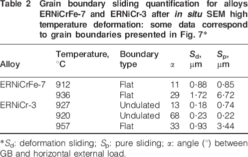
*Sd: deformation sliding; Sp: pure sliding; α: angle (°) between GB and horizontal external load.
In situ studies using XEDS and EBSD
Several in situ SEM experiments follow the material response to external conditions using XEDS and/or EBSD techniques.74, 75 When these two techniques are combined, the XEDS system first identifies the elements present, which are used as a filter for the crystallographic database. Then the EBSD pattern can be indexed, allowing phase identification and crystallographic information to be extracted. Therefore, the parallel use of XEDS and EBSD data provide a means to address the interrelating effects of local texture and chemical composition as well as providing a dramatic improvement in the reliability of orientation mapping results in materials with multiple phases.76 However, the time required to collect and process this data limits their use for in situ studies to relatively slow dynamic processes.
When heating and/or straining capabilities are combined with EBSD mapping, it is possible to study the crystallographic response to straining, either at high temperature, or just the crystallography of phase transformations. Thus, the study of texture evolution, orientation changes, grain boundary migration during static recrystallisation,77, 78 grain growth, orientation relationship development79, 80 and phase transformation81 are possible. Dedicated equipment, such as the modified SEM chamber door with a tensile stage attached to it shown in Fig. 8a and b, has been developed to allow in situ EBSD data collection during straining experiments.82 Compression and bending fixtures have also been implemented for this type of study (Fig. 8c and d). This instrumentation allows collecting data as presented in Fig. 8e and f, where inverse pole figure maps of AA 5754 sheet is shown before and after tensile loading to 2250 N corresponding to point B in the stress–stroke curve in Fig. 8g. The colour change within the grains reveals orientation change due to the large amount of dislocations. Figure 8g shows the stress versus stroke curve for the in situ tensile test of AA 5754 and the DIC quantified microstrain.
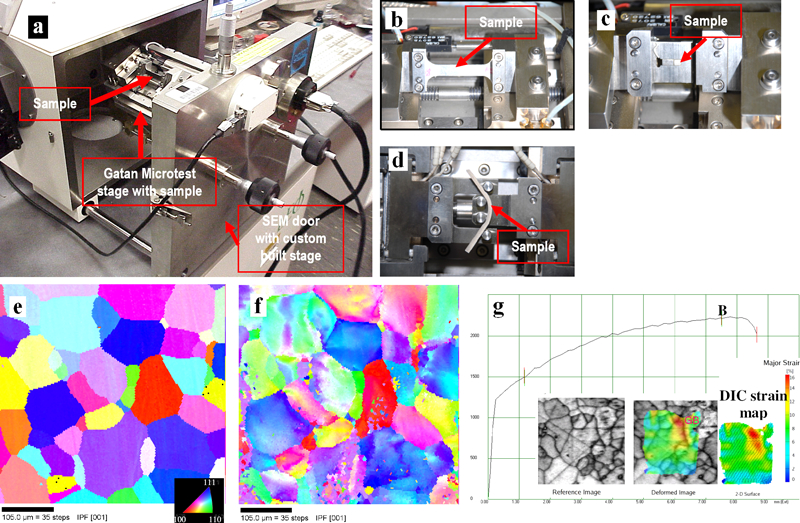
Microstraining system compatible with EBSD measurements. a SEM chamber door with attached microtensile stage; b–d tensile, compression and bending fixtures. Inverse pole figure maps showing grains in AA 5754 sheet e before and f after tensile loading to 2250 N (point B in stress versus stroke curve in g). g Stress versus stroke curve for in situ tensile test of AA 5754 and DIC quantified microstrain82
Figure 9 presents an in situ SEM phase transformation study for Ti.83 It is shown as an schematic illustration of hcp (α)–bcc (β) phase transformation of Ti during heating (Fig. 9a–c) and subsequent cooling (Fig. 9d–e). Figure 9f–h shows the SEM images during the in situ heating–cooling cycle. Figure 9i shows the superimposed pole figures from the indicated regions, revealing the Burgers orientation relationship between the α matrix and the acicular β particle at 882°C during the heating. Figure 9j presents the pole figures obtained by EBSD revealing the as received (α texture) and after heating (β texture). Figure 9k shows the lath structures post‐β–α transformation, separated by low angle grain boundaries. This experiment has made possible the visualisation of α‐Ti (hcp) transformation at 882°C to β‐Ti (bcc), and the Burgers orientation relationship development between both phases at such high temperature. The final lath shape morphology, together with the specific orientation relationship, revealed the shear dominated (martensitic) transformation mechanism.
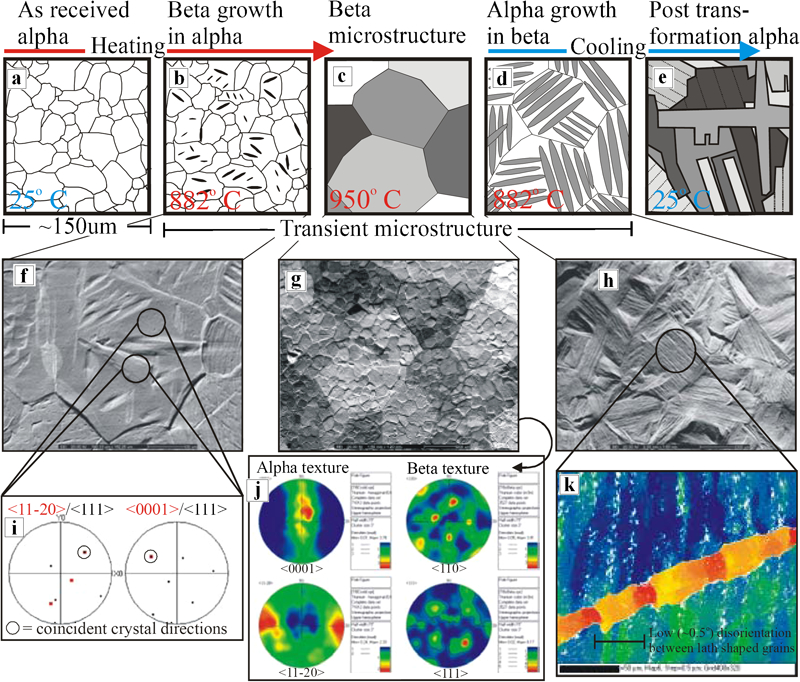
Schematic illustration of hcp (α)–bcc (β) phase transformation in Ti a–c during heating and d, e subsequent cooling. f–h SEM images during in situ heating–cooling cycle. i Pole figures indicating Burgers orientation relationship established between α matrix and acicular β particle. j Pole figures comparing as received α texture and after transformation β texture. k Lath structures post‐β–α transformation, separated by low angle grain boundaries83
FIB use for in situ experiments and materials characterisation
With the introduction of FIB to the materials community and the addition of such capability to the SEM, configuring what is known as the DB‐SM, a wide variety of possibilities were opened for materials characterisation, microfabrication and in situ experimentation. The destructive three‐dimensional characterisation by sequential material slicing using FIB followed by SE, BSE, XEDS or EBSD imaging complements in situ studies. For example, where three‐dimensional material analysis using DB‐SM can be performed in a fully automated manner.84– 87
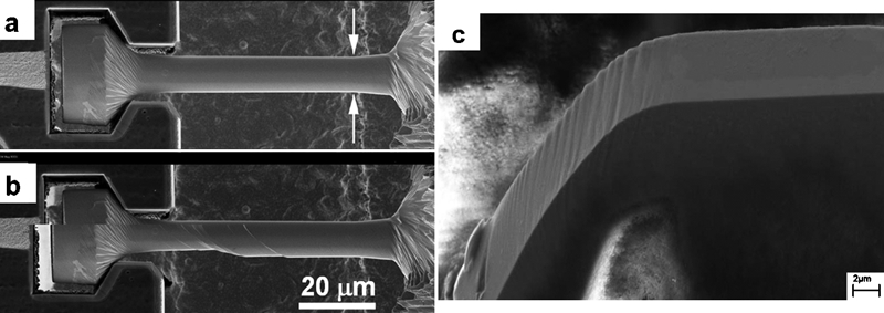
In addition, the potential of FIB as a supporting tool for in situ SEM experiments has been demonstrated by experiments where the samples with dimensions on the order of few microns were manufactured using FIB. In situ SEM compression and tension tests were conducted on cylindrical samples, fabricated using FIB.88– 90 In these experiments, the proposed microtension system, which uses a SiC grip and dog bone specimen, allows sample self‐alignment and reduces stress concentration, resulting in the gradual necking of the sample during the in situ tensile test, as shown in Fig. 10. Another example of FIB used for microsample fabrication is for the production of single crystal copper microbeams with 〈011〉 orientation and thicknesses between 1·0 and 7·5 μm, which were loaded with a nanoindenter, while recording force versus displacement curves.91 In this study, it was possible to identify a strong size effect on the dislocation behaviour, with the flow stress reaching ∼1·0 GPa for the thinnest samples.
In situ SEM welding
A pioneering study by MacCallum et al. 92 and Knorovvsky et al. 93 used a modified SEM to perform microelectron beam welding using the electron microscope beam to melt the material and perform the welding operation. The SEM modification allows an important increase in the beam power. A change in the W filament associated with small variations on the condenser lens currents and the use of a large limiting aperture (1000 μm) allows a 25 μA probe current to be obtained, which produces enough power to melt very small components. Several materials such as as Ni base alloys (LIGA), alloy steel, Chromel, Alumel and Tophe C have been successfully welded. The tested geometries included spot on plate, bead on plate, cross‐wires, gears on hubs and bar to bar butt welds. Figure 11 shows an example of microelectron beam welding of LIGA (nearly pure Ni) microgear to tool steel gauge pin shaft.93 Such applications are limited; however, they solve relevant technological applications related with MEMS applications.
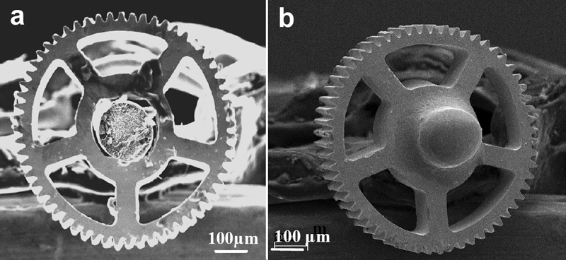
Electron beam welding of LIGA (nearly pure Ti) microgear to tool steel gauge pin shaft:93 weld produced using 1000 μm limiting aperture, 25 μA probe current, 30 keV accelerating voltage and 6 μm diameter spot
Perspectives for In situ SEM studies
The evolution of in situ SEM experiments is tightly linked to the evolution of the SEM and peripheral devices. The most relevant advances in SEM in last few years have been consistent improvements in spatial resolution, which today is below 1·0 nm, automation and signal processing, XEDS and EBSD detectors and the introduction of the DB‐SM.
The 50th anniversary of the first X‐ray map has recently been commemorated. Today automated X‐ray compositional imaging is possible by collecting a complete spectrum at each image pixel and forming a data cube called a spectrum image.94, 95 The introduction of SDD technology for XEDS has brought significant improvements in collection angle and count rate, without compromising the energy resolution. However, SDDs have poorer efficiency for photons with energy above 10 keV due to its reduced thickness. The XEDS mapping speed has been increasing; however, analysis of large areas continues to be a challenge.96 Therefore, parallel use of multiple XEDS detectors to improve the effective collection angle allows much faster data acquisition and may have an impact on in situ experiments requiring time resolved chemical information.97, 98 The XEDS mapping of non‐planar surfaces continues to be a challenge and some attempts to use multiple detectors to improve this type of analysis still present data interpretation limitations.99
The technical and scientific literature shows that EBSD applications continue to expand with the introduction of better processing software and faster and more sensitive detectors. Nevertheless, important areas such as strain quantification at the submicron scale continue to be a challenge and the limits of this field are yet to be determined.100 Another area where there is room for improvement is crystal rotation resolution, where some recent post‐processing methods show promising results.101 However, in some of these areas, including sample surface condition, the technique may be reaching some fundamental limits. However, with the much faster EBSD data acquisition and processing available nowadays, the use of such technique for in situ studies should expand allowing exiting science in the area of phase transformation crystallography.
Advances and widespread use of FIB and DB‐SMs are driving outstanding in situ experiments. Nowadays, in situ experiments involving FIB capabilities are moving towards smaller scale experiments and more fundamental problems. However, the possibilities are still almost unexplored, especially in the case of materials joining.
Sample size is a parameter that may define the scalability of the obtained results and the capability of the in situ test to reproduce the phenomenon of interest. Therefore, some experiments could or should be performed in small samples, but others may require larger ones to mimic the intended external conditions. In this sense, in situ SEM technology has grown in one direction, miniaturisation, where the resolution power of electron microscopy is best used. However, depth of field is another important advantage of the SEM technique, allowing the detailed observation of large and irregular surfaces with outstanding image sharpness. In this direction, some large SEM sample chambers have been built, which can fit large mechanical components or even a regular tensile machine. There are still vast opportunities for large scale in situ experiments to address countless engineering challenges.
Owing to their advantages when compared to the more traditional ex situ experiments, in situ studies are gaining in popularity among the scientific community. Along with such experiments, the integration of different characterisation techniques and/or tools is growing in popularity. Therefore, an increase on the integration of SEM systems with other techniques to compose sophisticated material science in situ experiments could be expected in the near future.
Finally, even in situ SEM experiments have not been as widely used by the materials joining community as they could be. This review demonstrates the unlimited opportunities behind this scientific approach to address fundamental and technological challenges related with welding and joining of conventional and new materials.