
Abstract
This paper presents the results of shear tests performed on Cu/In–48Sn/Cu diffusion soldered interconnections at the room and elevated temperatures of 373 and 423 K. Before the tests, the microstructure characterisation and chemical microanalysis of the joint area were performed. Termination of the diffusion soldering process led to the significant increase in the ultimate shear strength values. These values differed because of the type of the intermetallic phase that fulfilled the joined area: 11·2 MPa for [Cu6(Sn,In)5] and 28·5 MPa for [Cu41(Sn,In)11] phase. The shear tests performed at higher temperatures revealed a very good strength of the joints (9·8 MPa), especially for those with only the [Cu41(Sn,In)11] phase where fracture occurred inside the copper substrate. In the case of joints where unconsumed solder, [Cu6(Sn,In)5] and/or [Cu41(Sn,In)11], phases were present, the fracture surfaces observations allowed concluding that the crack propagated mostly through the intermetallic/solder interface or inside the intermetallic phase.
Introduction
The diffusion soldering technology is the joining technique which takes advantage of the intermetallic phase (IP) formation due to its good thermal stability. The intermetallics form also in the conventional soldering at the solder/conductor interface. In such a case, a thin and continuous IP layer is an essential requirement for good wetting and bonding, and it also improves the mechanical properties of such joint. Unfortunately, a too thick IP layer may degrade the reliability of the solder joint if the intermetallics form undesirable morphologies, like whiskers and scallops, which promote stresses inside the joined zone.1 Diffusion soldering is very frequently described as transient liquid phase bonding (TLP), although the resulting microstructure is usually a solid solution of the joined substrates. The fundamentals of TLP have recently been review by Gale and Butts,2 who concentrated on the mechanisms of the TLP including both microstructure and wettability aspects as well as specific engineering applications.
For the conventional solders, the working temperature is limited to 333–373 K below the soldering temperature (usually 493–533 K for Pb–Sn solders). For diffusion soldering, the thermal stability is much higher because the growth of the IP is fully controlled, and a very thin interconnection is totally fulfilled by the IP.3– 5 So far, several alloy systems have been designed and successfully used for diffusion soldering, among them Cu/Sn/Cu, 6 6,7 Cu/In/Cu8 and Cu/In–Sn/Cu.9
The mechanical strength of the interconnections is one of the most important parameters that should be controlled, especially in devices undergoing stresses and shakes. The paper presents the results of mechanical tests performed on the Cu/In–48Sn/Cu diffusion soldered interconnections combined with the microstructure and chemical composition characteristics. As the joints working in the electronic systems are usually endangered on the shear stresses, the shear test was chosen as a representative mechanical strength factor.
Experimental
Pure copper (99·999%) was used as joint material, and it was grinded and cleaned in an ultrasonic cleaner for 30 min. High purity components In and Sn (99·999 wt-%) were melted in appropriate amounts and cold rolled to obtain thin foils of In–48Sn (48 at-% of tin) eutectic alloy. The thin foil was clamped between two Cu pieces and diffusion soldered without any inert atmosphere (shear test at the room temperature) or in vacuum (shear test at 373 and 423 K).
The microstructure observations performed on both optical electron microscope and scanning electron microscope (SEM) required the preparation of the cross-section area.
The SEM observations were performed using a Philips XL30 microscope at accelerating voltage of 20 kV. Information about the chemical composition was collected by measuring the generated radiations of Cu Kα, In Lα and Sn Lα X-ray lines using the Link ISIS energy dispersive X-ray spectrometer (EDX) and subsequently quantified using Cu, In and Sn pure standards and ZAF correction procedure.
The shear test was carried using an Instron 6025 machine with displacement rate of 0·2 mm min−1 and maximum load of 1 kN. The tests were performed at room temperature and at 373 K. The sample geometry for the shear test together with the photo presenting the sample mounted in the Instron machine holder was presented elsewhere.9 The sample holder was constructed to ensure the occurrence of pure shearing stresses, and three samples for each soldering conditions (temperature/time) were mechanically tested.
Results
The detailed microstructure and chemistry characterisation of the diffusion soldered Cu/In–48 at-%/Cu joints before the shear test were previously described.10 This examination revealed that, depending on the temperature and the time of diffusion soldering, two phases can exist in the joint (Fig. 1). The η[Cu6(Sn,In)5] is formed as the first one in the temperature range of 453–493 K. After a longer time of annealing, the δ′[Cu41(Sn,In)11] phase starts to grow at the η/Cu interface, in which part of the tin atoms has been replaced by atoms of indium, and therefore, its stability changes from 621–859 to 473–859 K. In the 573–623 K temperature interval, the concurrent growth of η and δ′ was observed, but after a sufficiently long time, the soldering process was terminated with the only one δ′ phase in the joint. The presence of η and δ′ phases was confirmed using EDX analysis on the SEM and referred to the appropriate isothermal section of the Cu–In–Sn equilibrium phase diagram.10
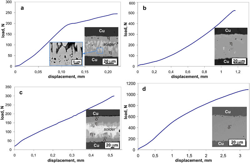
Load–displacement curves and SEM images of Cu/In–48Sn/Cu joints produced at a 473 K/3 h, b 473 K/3 days, c 573 K/5 h and d 573 K/3 days
Therefore, for this study, the existence of those phases was only randomly checked using EDX analysis on SEM. Four different types of joints resembling the various soldering temperatures and times were selected for the shear strength test. They are shown in Fig. 1 together with the typical load–displacement curves obtained due to the shear test. It can be seen from Fig. 1 that the value of load necessary to fracture the sample was dependent on the phases existing in the joint.
In the case when both η phase and unconsumed solder were present, the load was found to be 244 N (Fig. 1a), while for the soldering process to be completed and the joint consisted of only η phase, the load necessary for failure increased to 523 N (Fig. 1b). The same tendency was observed for the δ′ phase. After annealing at 573 K for 5 h (Fig. 1c), both phases together with unconsumed solder were present in the interconnection, and the load necessary for the sample failure was equal to 300 N, while annealing for 3 days (Fig. 1d) resulted in an increase in the load necessary for failure of more than three times (1086 N).
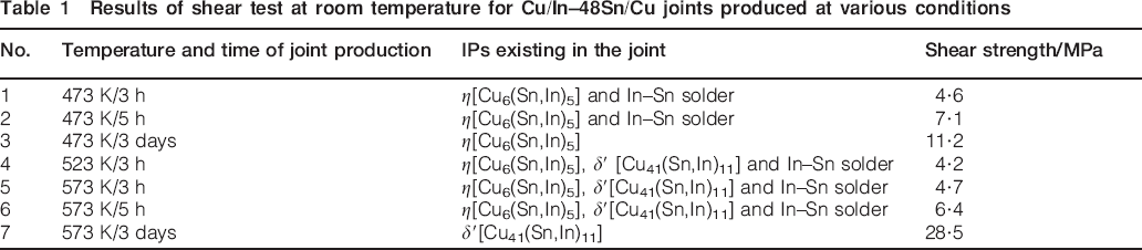
Table 1 contains the data concerning the conditions of joint manufacturing, the type of the IP detected and the corresponding values of shear strength for the Cu/In–48 at-%Sn/Cu joints. It is noteworthy that the ultimate shear strength (USS) increases with the increase in annealing time for the joints manufactured at 473 and 573 K. This is associated with the phases existing in the joint. One can easily see that the highest shear limit of 11·2 MPa (after annealing at 473 K) is in the case of only the η phase was present in the joint. The same tendency was noticed after annealing at 573 K when only the δ′ phase was identified in the joint (shear limit equal to 28·5 MPa).
Results of shear test at room temperature for Cu/In–48Sn/Cu joints produced at various conditions
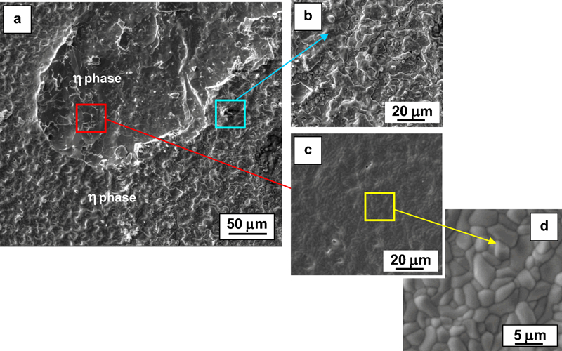
After the shear test, the samples were observed on the SEM. Figure 2 presents the typical micrographs of sample fractures obtained at 473 and 573 K after shorter (3 h) and longer (3 days) times of annealing. The rounded shape zones of plastic deformation were surrounded by areas possessing a characteristic crystalline character, which was especially visible at higher magnification. The microchemical analysis in the rounded shape zones of the samples annealed at 473 K for 3 h (Fig. 2a) revealed the existence of the η phase, while the chemical composition of the applied solder was found in the neighbourhood. Analogously, for the shorter annealing time at 573 K (Fig. 2b), the δ′ phase was present in the plastically deformed zones and unreacted In–Sn solder in the remaining part of fractured sample. In the case of samples annealed for 3 days, the η (Fig. 2c) or δ′ phase (Fig. 2d) was identified in the whole fractured area after diffusion soldering at 473 and 573 K.

Images (SEM) of Cu/In–48Sn/Cu joints diffusion soldered at a 473 K/3 h, b 573 K/3 h, c 473 K/3 days and d 573 K/3 days after shear test: higher magnification of some selected areas of joints is shown in boxes
From the point of view of the joint performance in the various devices, the joint should be characterised by good mechanical properties at elevated temperatures that are proper for service conditions of the joint. Therefore, the additional shear test was performed at 373 K for the joint produced at 473 K as well as the shear test at 373 and 423 K for the joints produced at 573 K. Having in mind that the best shear limit was previously obtained for only η or δ′ to be present in the joint, the applied time of annealing was long enough to transform the whole In–Sn solder into the IPs.
Table 2 contains all the details of the shear test performed at elevated temperatures. The values of the USS at 373 K for the joint manufactured at 473 K for 3 days and 2 weeks were rather similar and are equal to 9·5 and 9·8 MPa, respectively. In the case of the joints manufactured at 573 K for 1 and 2 weeks, the shear test performed at 373 K resulted in the sample failure not within the joined area. The strength of the interconnection was so high that the destruction appeared in the copper substrate fixed in the Instron handle. The same behaviour was observed after the test performed at higher temperature of 423 K.
Results of shear test at elevated temperature for Cu/In–48Sn/Cu joints produced at various conditions

Observations of the fractures after shear test indicated that, in all the samples, the η phase was present in both plastically deformed (see example in Fig. 3a and c) and brittle areas (Fig. 3a and b). Additionally, small grains with diameter of 5 μm and less with distinctly visible boundaries were found after soldering for 2 weeks (Fig. 3d).
Images (SEM) of Cu/In–48Sn/Cu joints diffusion soldered at 473 K for 2 weeks after shear test at 373 K: higher magnification of b brittle and c, d plastically deformed areas is also presented
Discussion
The first important information coming from the shear tests performed in the Cu/In–Sn48 at-%/Cu joints manufactured during diffusion soldering was that the temperature and time of soldering should be selected in such a way to have the whole solder material transformed into the IP(s). It can be noticed that the increasing values of the USS for samples with the same phase composition depend on the mutual proportion of these phases (compare in Table 1 no. 1 with 2 and 5 with 6), reaching the highest value for joints where the diffusion soldering process has been completed. Otherwise, the resulting value of USS is the lowest (4·2–6·4 MPa) regardless the fact that one or more IPs coexisted in the joints together with the unconsumed solder. Such a situation can be compared to that observed for conventional soldering. The shear strength of lead free solders, especially within the SAC group, as well as the relation between the intermetallic layer width and the joint shear strength in conventional soldering were the subject of many reports.11, 12 Mostly, these reports show the negative influence of the intermetallic layers formed at the pad/solder interface on the mechanical properties of the joints.13– 15 There are also works in which the impact of the wide layers of the IPs was not significant in terms of joint strength.16, 17 The influence of the layer width of η[Cu6Sn5] (after soldering) and η[Cu6Sn5] and ϵ[Cu3Sn] (after aging) obtained in leadless ceramic chip carrier surface mount solder joints with PbSn as solder material was described by Chan et al. 18 It was found that the increase in the η phase layer width resulted in a decrease in the joint strength in a linear way. The authors explained this phenomenon by the loss of tin from the solder material in favour of the growth of the intermetallics and by the changes in the IP layer morphology into a less irregular one. This all holds true as long as the crack propagation path goes through the PbSn solder. However, after longer times of annealing, it is expected to go through the PbSn/IP interface. Lee et al. 19, 20 reported that even small additions of copper to the lead free solders improved the joint strength and reduced the rate of degradation of the adhesive strength during thermal storage. It was caused by the presence of the Cu6Sn5 IP, taking different shapes depending on the copper amount. In our studies, better USS values give the joints with one IP instead of two. Termination of the diffusion soldering joints with solely δ′ phase resulted in the best values of USS equal to 28·5 MPa.
The observation of the surface fractures of the joints containing unconsumed In–Sn solder material showed the rounded shape areas of IP embedded in the matrix, identified as eutectic In–Sn alloy (Fig. 2a and b). This means that interfacial separation occurs between the solder and the IP. Such a behaviour results from the residual stresses existing due to the formation and growth of the new phase and also due to the irregular shape of the interface with the solder (Fig. 1a and c).
The fracture surfaces of the samples where only one IP was present (η or δ′) were characterised by a similar microstructure, both after the shear test performed at room (Fig. 2c and d) and elevated (Fig. 3) temperatures. The use of higher magnification revealed that failure of the sample within those areas occurred intergranularly, which was especially visible for the samples diffusion soldered for 2 weeks and subjected to shear test at 373 K. Moreover, the rounded shape areas having the chemical composition corresponding to the η phase are probably the voids coming from the solidification shrinkage and/or Kirkendall effect. The small grains of ∼5 μm in diameter are the evidence of their free surface, as clearly visible in Fig. 3d.
The observed dual η morphology, where the grains beside the Cu substrate were always substantially smaller than those in the central part of the joint (see enlarged box in Fig. 1a), allowed to assumed that the crack propagation in the joints where the diffusion soldering was terminated (there is no unreacted In–Sn solder) occurs primarily plastically through the interface between small and large grained areas. This interface was clearly visible due to the presence of the located voids.16 On the other hand, the areas with brittle fracture surfaces are attributed to the transgranular fracture through the large grains.
It should be emphasised that the shear test performed at elevated temperatures brought surprisingly good results. The ultimate shear stress at 373 K for the samples with only η phase or the η phase coexisting with δ′ was close to 10 MPa (Table 2). In spite of the fact that, in joints produced for longer time, both phases η[Cu6(Sn,In)5] and δ′[Cu41(Sn,In)11] coexisted, the contribution to the shear strength of the δ′ phase was not observable. Most probably, this was due to the relatively low thickness of this phase present next to the copper substrate. The crack propagated through the weaker η[Cu6(Sn,In)5] phase, which was proved by the EDX analysis of the fracture surfaces. Moreover, the test performed for the samples diffusion soldered at 573 K (where only the δ′ phase existed) resulted in the failure of the Cu substrate both at 373 and 423 K (Table 2) while the joint was not destroyed. This is very promising from the viewpoint of the joint application in the devices serving at the elevated temperatures. However, at this stage of research, we can only speculate that maybe such behaviour is attributed to the further diffusion processes, which can occur faster under loading, leading to the adhesion increase in the joint.
Summary
In this study, shear tests on the Cu/Cu interconnections obtained in low temperature diffusion soldering process using a eutectic alloy of indium–tin were carried out. The tests performed on the joints where the diffusion soldering process was not finished revealed that the fracture occurred through η/solder interface and the USS values grew with increasing thickness of the IP. The greatest value of 11·2 MPa was obtained in the joints fulfilled by the η phase and propagation of crack run at the fine and coarse grained microstructure interface (Kirkendall voids). On the other hand, the shear strength of the interconnection with two IPs and unconsumed solder was found to be lower than in the case of one IP. The best results in the mechanical tests showed the diffusion soldered joints containing only the δ′ phase. The shear tests carried out at elevated temperatures of 373 and 423 K did not cause reduction in strength, and the destruction of the samples took place outside the joint area.
Footnotes
Acknowledgements
This work was performed in the frame of the European Action COST 531 on lead free solder materials.