
Abstract
A three-dimensional finite element model of micro electron beam welding is developed where the Kanaya–Okayama heat source formulated in Part I of this work is used to represent the electron beam. The large number of process variables is grouped into two non-dimensional parameters, namely, Peclet number and relative beam penetration, and their effect is analysed numerically to arrive at the optimum conditions of microwelding. Based on the minimum heat input of the process, the optimum Peclet number is found to be 100, and the beam penetration is twice that of the weld depth. The optimum parameters obtained using the Kanaya–Okayama heat source model are similar to the previous findings using the exponential decay heat source model; however, the predictions of the temperature field in the solid as a result of microwelding are relatively lower in case of the Kanaya–Okayama heat source model because of the differences in distribution of heat into the condensed matter. The lower weld surface temperatures in microwelding using the electron beam suggest significantly less ablation than in laser beams.
Introduction
Welding at micrometre scales and below requires the use of higher intensity heat sources with their focussed spot sizes and small residence times. The challenges that are inevitably associated with employing high intensity heat sources are excess evaporation and poor quality welds.1 However, it is recently reported that volume heating is the key to avoid excess vapourisation at higher heat intensity levels and hence successfully weld at micrometre scales and smaller.2– 6 The adaptation of any such volumetric heat source to weld at micrometre scales has a huge potential to revolutionise welding applications in microelectromechanical systems, medical and aerospace industries.
Electron beams, owing to the ability of the electrons to penetrate a few micrometres into the material, can act as a volumetric heat source for microwelding applications.7 Treating electron beam as a volumetric heat source depends on selecting the right combination of beam parameters such as voltage, current, spot diameter and beam velocity based on the properties of the target material. The large number of process parameters involved necessitates developing a suitable numerical model that improves the prediction capability and decreases the experimental design costs.
An important step in the numerical modelling of micro electron beam welding (μEBW) is representing the volumetric heat distribution of the electron beam accurately. Many researchers have adopted simplified mathematical models to represent the electron heating of matter. Hwang and Na8 identified a square region of finite depth over which the beam rasters, as the heat generating volume in their domain, and solved for temperature field in the solid numerically. Knorovsky et al. 9 represented the electron beam heat source by considering a cylindrical volume with uniform heat generation. Both of the above mentioned models assumed the heat generation to be uniform across a volume and have not accounted for the spatial variation of heat intensity under the beam. Recently, Gajapathi et al. 5 represented the energy decay trend of the electron beam along the depth of the solid by an exponential decay heat source model. However, the electron energy decay does not really occur exponentially along the depth, and hence, considering such a heat source geometry in the numerical model would not provide a good representation of the practical situation.
The Kanaya–Okayama heat source model developed in Part 1 of this work, which is a closer representation of the three-dimensional heat distribution due to an electron beam, is used in this paper to carry out numerical simulation of μEBW; the numerical approach is similar to that developed by the authors in the past.4– 6 The current numerical model is validated by comparing the temperature field in two asymptotic cases, one in the region near the heat source and the other far away from it. The numerical model is then used to evaluate the effect of welding parameters that are grouped into two non-dimensional numbers, namely, the Peclet number and the relative beam penetration depth, on the evolution of temperature in the solid. The optimum microwelding conditions, in terms of Peclet number and relative beam penetration depth, are obtained based on the minimum heat input. The temperature field predictions are also compared between the Kanaya–Okayama model and the previously used exponential decay heat source model, and important differences are highlighted.
Mechanisms of heat transfer in μEBW
In μEBW, an electron beam is used to melt the material under the beam, creating a molten bead with a width similar to the beam width and a depth similar to the penetration of electrons into the condensed phase. A schematic representation of the process is shown in Fig. 1, where the heat source travels at speed U along the centreline. The shape of the heat distribution on the surface and along the penetration of the electron beam heat source is also pointed out in the same figure. The temperature field in the solid during the process can be obtained by solving the heat conduction equation.
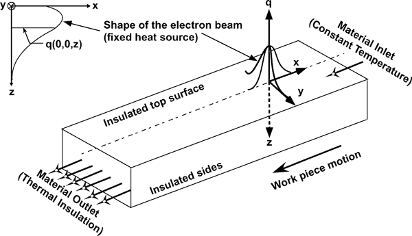
Schematic of model showing brick shaped solid, trend of heat distribution of electron beam that travels over solid and pertinent boundary conditions valid in moving reference frame
The hypothesis of continuum is valid at the micrometre scale considered in the present study; however, at small scales, special considerations might be necessary to model heat conduction. For scales approaching nanometres, heat transfer occurs quite differently, and a different phenomenological understanding of heat conduction is required to formulate the problem. Heat conduction in solids is described as the transport of energy by electrons and phonons, where the two carry the heat in different manners. Electrons play a major role in conduction in solids, whereas phonons are the only source of conduction in insulators.10 In the present problem, the electrons from the beam transfer their momentum and energy to the electrons in the substrate. In summary, the energy from the incoming electrons is used to heat the electrons in the body, which is then distributed (conducted away) by the interactions between electrons and phonons.
The conductions through electrons and phonons are to be dealt with separately if the length scales of the substance and the ‘residence time’ of the heat source are in the order of the mean free path and the mean free time of these energy carriers. The mean free path is defined as the distance between two successive collisions, and the mean free time is the time of rest between the two collisions. Electrons have a mean free path less than a few nanometres and a mean free time in the order of femtoseconds, depending on the energies of the electrons. On the other hand, the mean free path of the phonons ranges from nanometres to micrometres, and the mean free time is in the order of picoseconds to nanoseconds, depending on the temperature.10 The length scales involved in the present research are >100 nm, and the weld speeds are not high enough to cross the residence time limits of nanoseconds. Hence, the study of ballisitc behaviour of electrons is not important here. The heat conduction can be assumed diffusive, and the macroscopic Fourier heat conduction is valid. Nevertheless, the applicability of such a model for nanowelding or joining semiconductor materials, where electrons and phonons play equal role in energy transport, requires developing of appropriate nanoscale heat transport models.
The governing heat conduction equation in a coordinate frame attached to the moving heat source and the boundary conditions representative of semi-infinite solid are described by the authors in their previous work.4– 6 The FWHM of the Gaussian function, representing the power density distribution on the target surface, is considered as the beam diameter d. The other important physical processes occurring during welding such as melting, evaporation and effect of temperature dependent thermophysical properties of the material are outside the focus of the current study.
Numerical analysis
The numerical model of μEBW in this analysis is similar to that developed earlier4, 5 but using the Kanaya–Okayama heat source developed in Part 1 of this work, which is a closer representation of the electron beam. The finite element based numerical package COMSOL Multiphysics is used to solve the Fourier heat equation in moving coordinate system. The computational domain here is only one-half of the brick shaped geometry, shown in Fig. 1, owing to the symmetry of the practical situation along the centreline. Meshing of the subdomain is carried out following the guidelines reported previously.4 Figure 2 depicts a typical grid used in the current analysis. For the example considered in this work, the numerical solution is obtained for silicon as the material, with thermophysical properties considered constant and listed in Table 1.
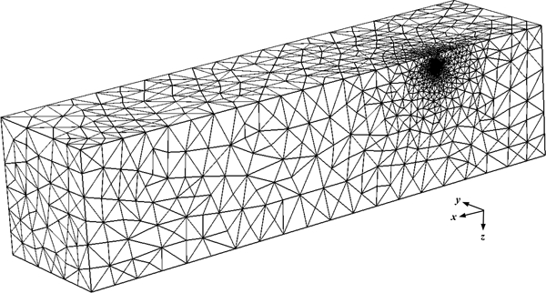
Computational domain meshed with non-uniform tetrahedral elements
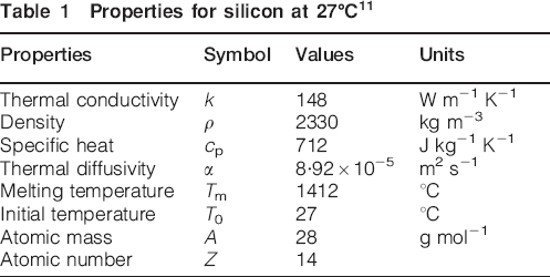
Properties for silicon at 27°C11
Validation of numerical model
The current numerical model can be validated against the well known point heat source solution developed by Rosenthal12 by modelling a very concentrated volumetric heat source. Rosenthal's solution, however, predicts infinite temperature at the origin of the point heat source and hence cannot be compared with the numerical solution close to the beam. The temperature profile under the beam is analysed by solving the limiting case in which heat conduction is negligible, as proposed by Gajapathi et al. 5
Far field temperature
The temperature field in a semi-infinite solid of constant properties due to heat conduction from moving point heat sources is provided by Rosenthal12 as
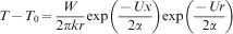
To represent the volumetric heat source of the present model as a point heat source, the beam diameter and the maximum electron penetration range are assigned small values of 0·2 and 0·1 μm respectively. The meshing procedure suitable to resolve such concentrated point heat source, described in Ref. 5, is followed. For comparing with the analytical solution, the beam power and the beam travelling speed are kept constant at 10 W and 450 m s−1 respectively, and the properties of silicon shown in Table 1 are used.
The numerical solution with the concentrated heat source, resembling a point heat source, is compared against its analytical solution given in equation (1); the variation of temperature along the centreline on the surface of the solid is compared in Fig. 3. The temperature field obtained using the numerical approach, represented as black dots in the same figure, shows good agreement with the analytical solution. The break in the continuous line, as seen in Fig. 1, is around the centre of the point heat source where the temperature rises to infinity.
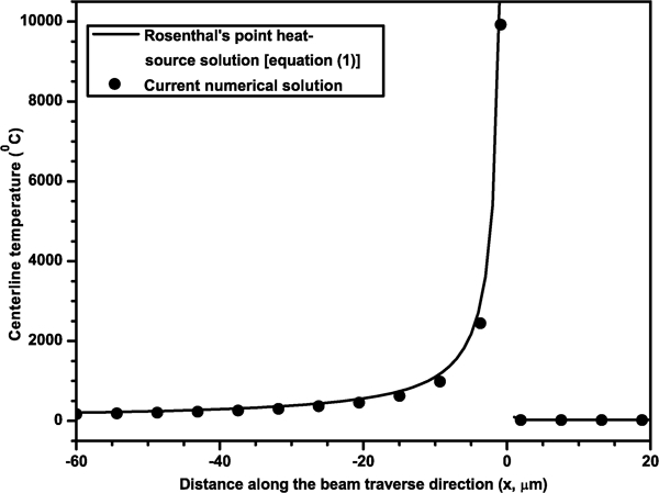
Temperature variation along centreline of solid is compared between Rosenthal's point heat source solution and current numerical model for W = 10 W, U = 500 m s−1, k = 148 W m−1 K−1, d = 0·2 μm and R = 0·1 μm
Temperature field near beam
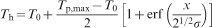
The temperature field near the beam can be analysed analytically for the asymptotic case of fast moving heat source. In this case, the Fourier heat equation reduces to an ordinary differential equation after neglecting the heat diffusion terms. The solution methodology described previously5 is followed in this work to obtain the maximum temperature distribution analytically in the solid. It is to be noted here that in the absence of heat diffusion during the process, the temperatures calculated are the highest values that can be attained for the given welding conditions. For the Kanaya–Okayama heat source model, the variation of asymptotic temperature Th along the beam traverse direction (x axis) and at the depth of peak electron energy deposition is derived as
Numerically, the asymptotic case of negligible conduction can be represented by considering an artificially low thermal conductivity of the material.3, 5 A value of k = 0·01 W m−1 K−1 is chosen in this study so that the temperature field reaches its asymptotic maximum and becomes insensitive to any further decrease in thermal conductivity.
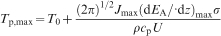
For moving heat sources, the non-dimensional Peclet number (Pe) is used as a metric to define how fast the supplied heat diffuses into the material relative to the travel speed of the heat source. The Pe can be defined as

The variation of Th is compared between the analytical solution in equation (2) and the numerical model with higher Pe value, as shown in Fig. 4; a good agreement is found between the two. Due to the absence of heat conduction during the process, the maximum temperature rises until the process peak temperature and does not fall after the beam passes over.
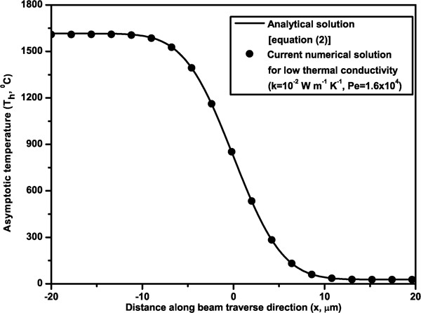
Temperature variation along centreline of solid ignoring conduction is compared between analytical solution in equation (2) and current numerical model for W = 10 W, k = 0·01 W m−1 K−1 and Pe = 1·6×104
Optimal beam voltage and beam travelling speed
The two critical parameters of μEBW are the beam voltage that governs the beam penetration R relative to the maximum melting depth zm and the beam travel speed represented by Pe of the process.5 The numerical model of μEBW using the Kanaya–Okayama heat source is used to obtain the optimum process parameters.
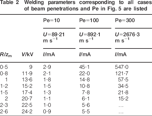
The optimum electron beam voltage and Pe desired to obtain a microweld of given melting depth is decided by selecting the process with the least heat input.5 The heat input in welding can be defined as the relative amount of energy supplied per unit length of the weld:14 HI = VI/U. The beam voltage of the process is varied to obtain different electron penetrations R, and the beam current is adjusted suitably so that the maximum melting depth zm of all the processes remains constant at 2·5 μm. A constant beam diameter of 10 μm is chosen for all the cases, and the values used for welding parameters such as voltage, current and beam velocity in each case are listed in Table 2. The heat inputs of such processes are compared at three different beam travelling speeds corresponding to Pe = 10, 100 and 300 in Fig. 5.
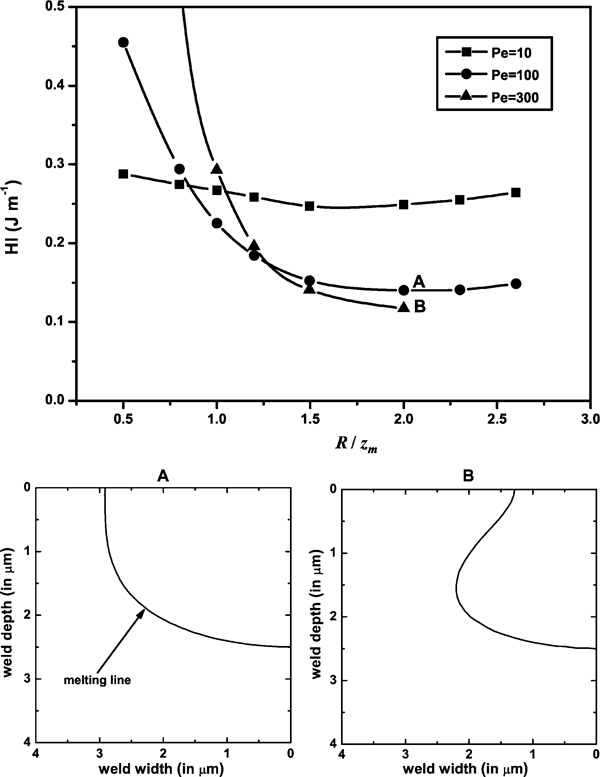
Variation of heat input with relative electron penetration range for three different Pe processes of 10, 100 and 300: weld cross-sections having same weld depth of 2·5 μm are shown for specific processes marked as A and B
Welding parameters corresponding to all cases of beam penetrations and Pe in Fig. 5 are listed
The higher heat input values for the processes having Pe = 10 in Fig. 5 are because of the large amount of heat being quickly diffused outside the weld region. The electron interactions and hence the increase in electron range are secondary in such heat diffusion dominated processes due to which the heat input curve is close to being straight. There is a significant drop in the heat input curve as the Pe of the process is increased to 100. Moreover, it is observed that the heat input is minimum, corresponding to the relative electron penetration range of R/zm = 2. The high heat input requirements for smaller electron penetrations (R/zm<2) can be attributed to the large dependence on heat conduction to propagate the electron energy until the melting depth, whereas at larger electron penetrations (R/zm>2), high energy electrons travel beyond the melting depth, causing unwanted heating of the additional material volume.
The processes with Pe beyond 100, for example, Pe = 300, do not result in any significant gain in heat input especially at larger electron penetrations (R/zm>1·2), as seen in Fig. 5. The weld cross-sections are compared between the processes with Pe = 100 and Pe = 300, corresponding to R/zm = 2 in the same figure. It is observed that the Pe = 300 process with a slightly lower heat input also has a smaller weld cross-section as compared to the process with Pe = 100. For the same electron penetration, the processes with higher Pe result in less heat diffusion, and hence, smaller weld cross-sections are obtained.
Comparison of Kanaya–Okayama and exponential decay heat sources
Temperature variation along depth
The temperature variation along the depth is compared between the Kanaya–Okayama and exponential decay heat source models in Fig. 6a and b for three different processes with Pe 1, 100 and 1000. The beam spot size and voltage are kept constant for all the processes. The beam current is varied such that all the processes produce the same maximum melting depth of 2·5 μm for this example. Along the vertical axis of the plot, the temperature excess of the initial condition is normalised with respect to the melting temperature gradient, and the depth of the solid is represented on the horizontal axis by normalising it with respect to the maximum electron penetration range. Numerical simulations have been carried out separately for both heat source models at different Pe; the material properties of silicon in Table 1 are used.
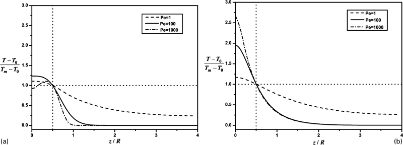
Variation of normalised maximum temperature along depth in non-dimensional form for processes with Pe = 1, 100 and 1000 is compared between a Kanaya–Okayama heat source model and b exponential decay heat source model: melting depth is kept constant at 2·5 μm and relative beam penetration is 2
For a process with constant Pe, it is observed that the Kanaya–Okayama heat source model predicts lower temperatures at any given point along the depth of the material compared to the exponential decay heat source model, as seen in Fig. 6. This can be attributed to the difference in electron energy decay behaviour of the two models. For the high Pe process of 1000, the Kanaya–Okayama heat source model obtains the peak temperature underneath the surface due to its inherent heating characteristics and also the high Pe causing the heat distribution trend to stand out. The exponential decay heat source model, due to its nature of depositing the maximum of its incoming energy on the surface, produces relatively larger temperature difference within the molten region.
Maximum temperature on surface
The maximum temperature at the weld surface Ts,max for the processes with different Pe is compared between the Kanaya–Okayama and exponential decay heat source models in Fig. 7, where the maximum melting depth is kept constant at 2·5 μm. The beam voltage is chosen such that the electron penetration range is twice the melting depth for all the cases. The material properties of silicon in Table 1 are used for the numerical simulations. It is observed in Fig. 7 that the maximum temperature of the process corresponding to the Kanaya–Okayama heat source model is smaller in the entire regime of Pe as compared to the exponential decay heat source model. This is because the maximum energy dissipation in the Kanaya–Okayama heat source model occurs underneath the surface, leading to less heating of the surface. The difference in maximum temperatures between the two heat source models becomes more prominent at higher Pe, as seen in Fig. 6, as the significance of heat diffusion decreases.
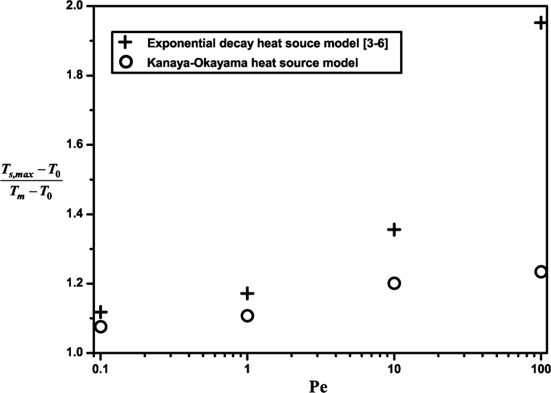
Effect of Pe on normalised surface maximum temperature is compared between Kanaya–Okayama heat source model and exponential decay heat source model: maximum melting depth is constant at 2·5 μm and electron penetration range is twice melting depth for all processes
Discussion
The optimum welding parameters obtained in case of the current Kanaya–Okayama heat source μEBW match that of the exponential decay heat source model reported in Ref. 5. A Pe of 100 has been reported as ideal by both models. Moreover, the optimal electron penetration variable in the previous model is reported as 0·8–1·2 times the maximum melting depth,5 for which the equivalent relative electron penetration range (R/zm) can be calculated as 1·8–2·8. In this work, the optimal electron penetration range is obtained as twice the maximum melting depth, which falls in the range reported earlier.
Previous study of μEBW using the exponential decay heat source model showed that the volumetric heating source produces lower weld surface temperatures as compared to the surface heating sources.5 The present study using the Kanaya–Okayama heat source model confirms this finding and further suggests that the surface temperature falls even lower as the peak of the incoming electron energy deposition occurs underneath the surface. Hence, the electron beam can be used at very high heat intensity levels that are necessary to carry out microwelding, as opposed to the surface heating sources such as laser beams that result in excessive ablation.
The length scale chosen to define Pe in this study is the beam diameter, based on which the optimum Pe is found to be 100. Such a consideration is valid when the length scale of beam diameter is of the same order of magnitude as the beam depth. The optimum Pe is expected to increase when the beam diameter is chosen much larger than the weld depth.
The current numerical model is not valid in the regime of welding conditions that cause keyhole formation. For example, for the weld described in plot A of Fig. 5 with weld parameters V = 20·65 kV, I = 6·08 mA, U = 892·1 m s−1 and d = 10 μm, there is no keyhole expected. However, if the voltage is reduced to 2 kV and the current increased to keep the same heat input, the electrons penetrate only ∼10% of the melt, leading to very high surface temperatures and most likely resulting in keyhole formation, leading to incorrect model predictions.
Conclusions
This work presents for the first time a numerical and analytical treatment of μEBW using the Kanaya–Okayama heat source model. This model applies to a desired weld penetration mode involving negligible evaporation and the absence of a keyhole. The calculations performed here use a realistic heat source model to confirm that it is possible to carry out μEBW in situations considered impossible for lasers or electron beams in keyhole mode.
The numerical model of μEBW predicts the temperature distribution in the solid for different choices of beam scanning speed and acceleration voltage. This analysis indicates that the peak temperature in the substrate is always lower than previous predictions using an exponential decay model of heat source; the difference is very clear at Peclet numbers above 100, while it is negligible below 0·1.
The sensitivity study performed here indicates that the optimum voltage has an interaction volume twice as deep as the desired weld penetration. The optimum beam velocity corresponds to a Peclet number of 100. These optimum values are obtained considering low heat input and adequate controllability. These values, obtained using the Kanaya–Okayama heat source model, are similar to those predicted previously using the exponential decay heat source.
Footnotes
Acknowledgements
This work was partially supported by the Natural Sciences and Engineering Research Council of Canada (NSERC).