
Abstract
A gold–aluminium material combination is typically employed as an interconnection for microelectronic devices. One of the reliability risks of such devices is that of corrosion of aluminium bond pads resulting from the galvanic coupling between an aluminium bond pad and a gold wire. The research presented in this manuscript focuses on studying bond pad corrosion by selecting an appropriate model system and a dedicated set of electrochemical and analytical experimental tools. Taking into account the complex three-dimensional structure and the small dimensions of Au–Al interconnections (around 50-100 μm), a dedicated and novel experimental approach was developed. Au–Al covered silicon chips were developed under clean room conditions. Three-dimensional electrodes were mimicked as flat, two-dimensional bond pad model systems, allowing the use of microelectrochemical local probe techniques. Thin gold films were applied on Ti–Al covered silicon surfaces, and their morphology and electrochemical behaviour were analysed using the localised electrochemical cell, scanning vibrating electrode technique, scanning electron microscopy–energy dispersive X-ray spectroscopy, scanning electron microscopy–focused ion beam and Auger electron spectroscopy. The results revealed that the electrochemical behaviour of thin gold films was influenced by the underlying metal layers and the microstructural changes during heat treatment. The effect of the underlying layers on the electrochemical properties of the top gold layer was attributed to a mixed potential behaviour and microgalvanic interactions, which was more pronounced after heat treatment. Overall, the current experimental approach can be employed to study the mechanism of electrochemical events that are occurring on metallic interconnections in different electronic devices.
Introduction
Gold–aluminium interconnections are used in microelectronic devices in which Au wires are connected to Al metallisation pads. Al bond pads, being unpassivated, are vulnerable to corrosion. One of the most likely reasons for corrosion is macroscopic galvanic coupling between an aluminium metallisation pad and a gold wire. Additional local corrosion issues are related to the effect of the ball bonding process. This process includes the microwelding of gold wires to an aluminium metallised silicon chip using ultrasonics, moderate device preheating and force to initiate the joining of a gold ball to an aluminium pad. The impact of the ball bonding process can result in reliability issues due to microstructural changes, i.e. the formation of Au–Al intermetallic compounds (IMCs) across the interface upon heating. Intermetallic compounds can lead to severe local microgalvanic corrosion and, in the end, to the loss of ball metallisation contact.1–6 An example of Al bond pad corrosion is shown in Fig. 1.
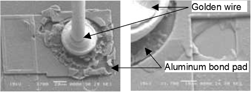
Typical example of aluminium bond pad corrosion by Au–Al galvanic interaction
A common approach to the study of the mechanism of bond pad corrosion is that of employing reliability experiments on the devices at high external stimuli, such as moisture, temperature and voltage.7–9 These stimuli are intended to accelerate the failure mechanism. Traditionally, these acceleration factors are determined by extrapolation of the test results over a wide range of the external stimuli, assuming that the failure mechanism does not change. In this approach, it is often assumed that stimuli do not interact with each other. However, this approach might become ambiguous under certain condition, e.g. when a product heats up due to power dissipation as a consequence of an applied electrical potential. Nowadays, the scientific field of corrosion technology and electrochemistry is experiencing a scientific revolution due to the development of local probe techniques, which enable the study of the relation between microstructure and corrosion properties at the micrometre scale. However, it is difficult to study the local electrochemical behaviour on the three-dimensional surface of the wire–bond interconnection. In the current work, a novel experimental approach to study bond pad corrosion was implemented. Two-dimensional model systems for the wire–bond pad interconnections were manufactured under clean room conditions. Thin Au films were applied on Ti–Al covered silicon surfaces using plasma vapour deposition (PVD). Local electrochemical behaviour of these model systems was analysed for the first time to our knowledge using local electrochemical techniques.
Experimental
Material preparation and heat treatment procedure
Three different types of samples were manufactured. A schematic representation of the samples is presented in Fig. 2. The description of the samples is as follows.
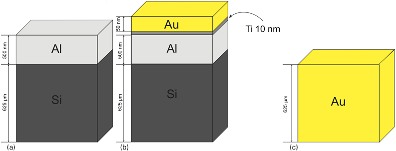
Schematic drawing of a Al covered (sample 1), b Au–Ti–Al covered (sample 2) silicon surfaces and c pure Au (sample 3) substrates
Sample 1: Al covered silicon wafer surfaces (NXP Semiconductors, The Netherlands)
Silicon wafers with a natural oxide layer (p type, boron; orientation: 1-0–0, resistivity of 2-5 Ω cm, thickness of 525±15 μm, diameter of 100 mm) were used. A 500 nm Al layer was deposited using PVD system (MRC Eclipse Mark IV, USA). Targets of analytical grade Al (99·9%) were used.
Sample 2: Au–Ti–Al covered silicon wafer surfaces (DTU Danchip, Denmark)
Silicon wafers with a natural oxide layer (p type, boron; orientation: 1-0–0, resistivity of 2-5 Ω cm, thickness of 525±15 μm, diameter of 100 mm) were used. A Ti layer was applied on the Al layer in order to improve the adhesion of the Au layer to the Al layer. Al, Ti and Au layers were deposited using a PVD system (MRC Eclipse Mark IV, USA) during consecutive runs respectively. Targets of commercially pure Al, Ti and Au were used. The thicknesses of the Al, Ti and Au layers were 500, 10 and 50 nm (standard deviation, 10%) respectively.
Note that the intermediate Ti layer was added in order to improve adhesion between Au and Al at the Au/Al interface. The presence of the Ti layer might influence the interdiffusion between Al and Au. During the current study, the authors have also PVD processed the Au layer directly on top of the Al layer. However, adhesion of the Au layer directly applied on the Al layer was considered insufficient because of apparent delamination. While this study was not aimed to optimise the PVD process conditions, further studies may focus on the feasibility and fine tuning of the PVD application process for direct application of Au on Al without the need for an intermediate Ti layer.
Sample 3: Pure gold sample
The wafers were diced into (3×3 mm) sample pieces suitable for the local electrochemical measurements. Different sets of samples were heated for the following temperature–time combinations: 170°C for 4 h, 225°C for 10 min and 300°C for 4 h. The first two temperature–time combinations were selected to represent the most important heating steps during the device manufacturing process, e.g. moulding (170°C) and soldering (225°C). Heating at 300°C was chosen in order to observe excessive microstructural changes leading to localised regions of significantly different electrochemical nature to be observed with electrochemical local probe techniques.
Experimental techniques
Scanning electron microscopy–energy dispersive X-ray spectroscopy
The scanning electron microscopy–energy dispersive X-ray spectroscopy (SEM-EDS) (JEOL JSM 6500F) technique was used in order to obtain information about the surface topography and its chemical composition. Based on an interaction volume simulation (Monte Carlo simulation), an accelerating voltage of 4 kV was used during the SEM-EDS analyses. The accelerating voltage was determined to cover an interaction depth of 50 nm of Au.
Scanning electron microscopy–focused ion beam
The focused ion beam (FIB) workstation (LEO 1540 EsB, Zeiss) was used to study the morphological and chemical depth profile of the surface. The FIB technique uses a Ga+ ion beam with a minimum diameter of 5 nm for micromilling the surface layer.
Auger electron spectroscopy
Auger electron spectroscopy (AES) (PHI 650 SAM with a LaB cathode) was used to measure the chemical depth profiles on the Au–Ti–Al covered silicon wafer surfaces. In its basic form, it provides compositional information using a broad focused electron beam probe. To obtain information on the variation in chemical composition with depth below the surface of a sample, it was necessary to gradually remove material from the surface region being analysed while continuing to monitor and record the Auger spectra. This controlled surface etching of the analysed region can be accomplished by simultaneously exposing the surface to an ion flux, which leads to sputtering (i.e. removal) of the surface atoms. Sputtering involved directing a beam of Ar ions with kinetic energy of 5 keV towards the sample.
Localised electrochemical cell
The microcell technique (Dual Scope, EC microcell, Denmark) was used to study the local corrosion behaviour. The cell consists of an electrochemical head containing the solution, counter and reference electrodes, which is attached to the carousel of an optical microscope. The cell is connected to a pipette (tip diameter of 300 μm) that makes contact with a local region of the working electrode (i.e. the sample). After positioning the microcell tip onto the specimen surface, the corrosion potential value E corr was measured for 10 min and then the potentiodynamic polarisation curves were taken. Potentiodynamic polarisation curves were measured relative to a Ag/AgCl reference electrode at a scan rate of 1 mV s−1 and started near the E corr. Cathodic and anodic scans were measured separately to prevent an effect of prepolarisation history. All potentials were converted to the values relative to the standard hydrogen electrode (SHE), i.e. E SHE = E Ag/AgCl+0·197 V. All measurements were carried out at a room temperature of 22±1°C. The lateral resolution of the technique is determined by the dimensions of the pipette tip (diameter of 300 μm). A 3 mM NaCl solution was used representing an average surface concentration of NaCl after fingerprint contamination.
Scanning vibrating electrode technique
The scanning vibrating electrode technique (SVET) (Applicable Electronics Inc., MA, USA) was used to measure the evolution of corrosion in an aqueous solution with high spatial resolution. The microelectrode consisted of an insulated Pt/Ir (80%∶20%) wire with only its tip exposed to the solution. The probe was platinised in order to produce a spherical platinum deposit with a diameter of 10-20 μm. The mean distance between the microelectrode and the sample surface was 100 μm. The vibration amplitude was 20 μm. Ionic current flow in the electrolyte results in a potential gradient within the electrolyte. This potential gradient is measured by the vibrating probe and resolved by two phase sensitive detectors into a voltage vector represented by magnitude and direction. The voltage vector is converted into a current density vector using calibration data generated from a separate experiment (calibration involves generation of a known current density from a point source calibration electrode) and electrolyte conductivity. From the measured current density vector distribution, both the magnitude and direction of the current flow can be mapped and local anodic and cathodic sites resolved. A video camera connected to an optical microscope is introduced into the system both to establish the probe to sample distance and to follow the movement of the vibrating electrode over the sample during its operation.
Results and discussion
Surface analysis of Al and Au–Ti–Al covered silicon wafer surfaces
In order to study the electrochemical behaviour of Al and Au–Ti–Al covered silicon wafer surfaces, the surface morphology of the chips was analysed using SEM-EDS. A typical top view SEM image of an Al coated silicon wafer surface is shown in Fig. 3.
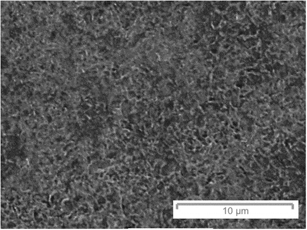
Image (SEM) of Al covered silicon wafer
The SEM images of Au–Ti–Al coated silicon chips are shown in Fig. 4. Almost no difference was observed between the surfaces of untreated samples and those heated at 170°C. Small spherical particles were uniformly distributed over the surfaces of both samples. However, surface imperfections in the outer Au layer (represented by black dots in the SEM image of Fig. 4a) were observed on the surface of the untreated sample.
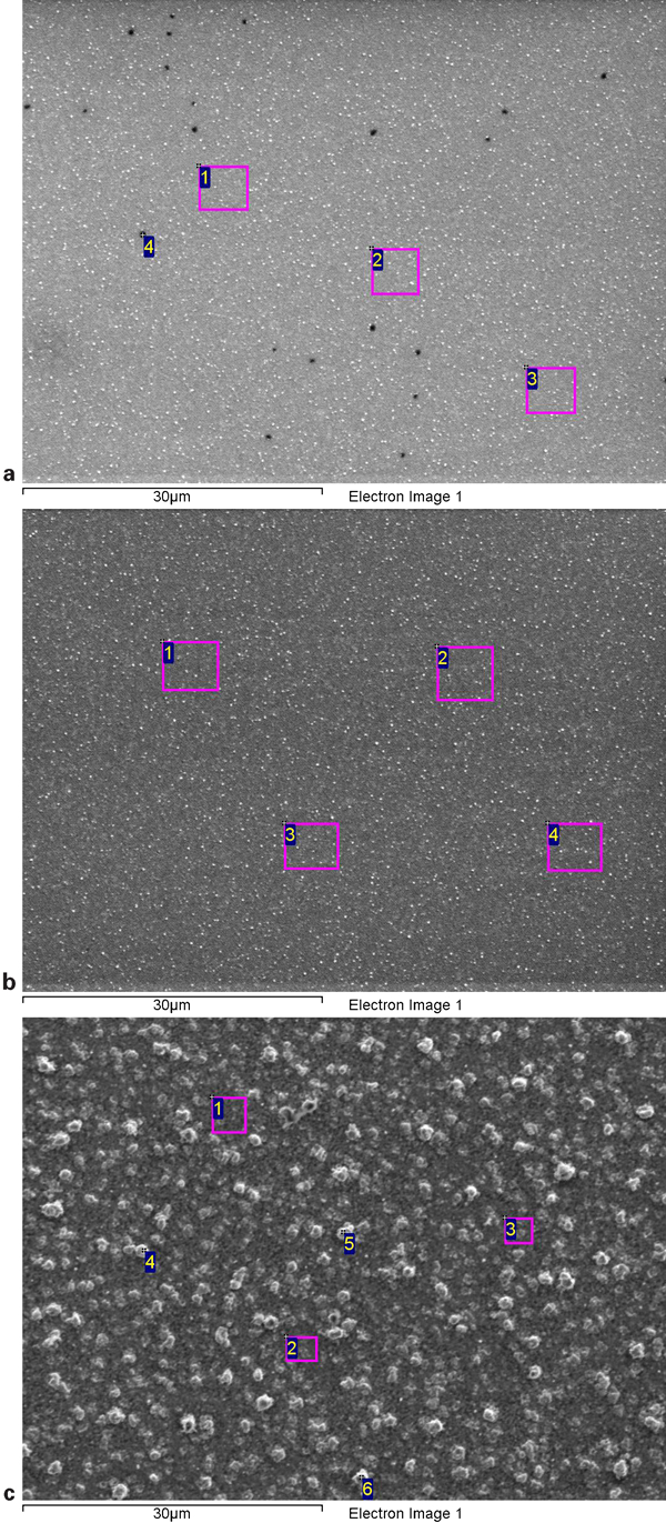
Images (SEM) of Au–Ti–Al covered silicon wafers
As shown in Fig. 4c, annealing at 300°C modified the surface structure to a large extent. The size of the particles had clearly increased. The chemical composition of the surface was analysed by SEM-EDX using an accelerating voltage of 4 kV. Average areas of ∼36 μm2 were analysed. The average weight percentages of the detected elements are presented in Table 1.
Elemental analyses of Au–Ti–Al covered silicon chip studied by EDS, accelerated voltage 4 kV
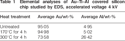
Up to 95%Au (standard deviation, 2%) was detected on untreated samples and those heated at 170°C. Unexpectedly, 5%Al (standard deviation, 0·1%) was found on the untreated samples and those heated at 170°C. In order to reveal the origin of the Al on the top surface, depth profiling was performed on the untreated Au–Ti–Al covered silicon chips using AES. Compositional information on an area of 9 μm2 is presented in Fig. 5.
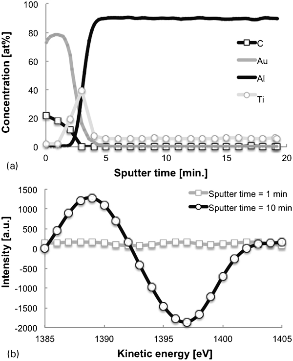
a Auger electron spectroscopy profiling of untreated Au–Ti–Al covered silicon chips and b aluminium KLL spectra at different sputter times (Al peak at 1388 eV apparent after 10 min of sputtering)
The depth profiling of the Au–Ti–Al covered silicon wafer surfaces is shown in Fig. 5a. The top layer was composed of gold and carbon (contamination) followed by a titanium layer. A thick aluminium layer was detected underneath a titanium layer. These results were in agreement with the deposited structure: thin Au and Ti layers (50 and 10 nm respectively) were initially applied onto a relatively thick (500 nm) Al layer (Fig. 2, sample 2). In order to check for the presence of aluminium on the top surface, the Al KLL spectra were obtained after 1 and 10 min of sputtering. The results are shown in Fig. 5b. As observed, after 1 min of sputtering, no Al was detected at the outer region of the sample. The results demonstrate that aluminium measured on the untreated surface originated from the surface defects as shown in Fig. 4a.
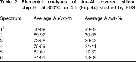
Annealing at 170°C for only 4 h did not change the surface concentration of the elements, whereas annealing at 300°C for 4 h altered the percentage of Al and Au significantly (Table 1). This indicates an interdiffusion effect of aluminium and gold taking place during the heating process. The EDS analyses showed that the weight percentage of Au was significantly larger at individual particles (Table 2, spectra 4-6) compared to the average value over the surface (Table 2, spectra 1-3). The Au enriched IMCs were formed during annealing at 300°C.
Elemental analyses of Au–Al covered silicon chip HT at 300°C for 4 h (Fig. 4c) studied by EDS
The formation of the IMCs was clearly seen on the images obtained via FIB-SEM and shown in Fig. 6.
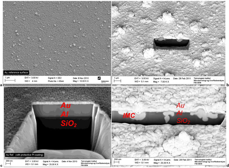
Cross-sectional images of Au–Ti–Al covered silicon chips using FIB
Clear separate layers of Au, Al and Si can be distinguished in the cross-section of the untreated sample (Fig. 6a and c). The formation of the IMCs is obvious after annealing for 4 h at 300°C (Fig. 6b and d). An interesting feature is the diffusion of Au into the Al layer, predominantly at the location of the IMCs (Fig. 6d). This is in agreement with the latest research in Au–Al thin film diffusion couples, where convincing evidence for Au being the predominant diffusant in this system was demonstrated.10,11,12
Microelectrochemical potentiodynamic polarisation analyses of Au–Ti–Al covered silicon wafer surfaces: MC technique
Local corrosion behaviour of the samples was analysed using an electrochemical microcell and was compared to that of pure gold. Potentiodynamic polarisation curves were measured relative to a Ag/AgCl reference electrode in 3 mM NaCl. An important parameter to take into consideration is the corrosion potential value E corr, which is the potential of a corroding surface in an electrolyte relative to a reference electrode. For a multicomponent electrode surface, E corr represents a mixed potential. Since Au acts as a cathode in the Au–Al galvanic couple, only the cathodic polarisation behaviour was measured. Polarisation curves of pure gold and the Au–Ti–Al covered silicon wafer surfaces, untreated and annealed, are shown in Fig. 7a. The E corr of 410 mV was measured on the surface of pure gold. In contrast, a corrosion potential of −350 mV was measured on the surface of the untreated Au–Ti–Al covered chips. The results reveal that the measured potential on Au–Ti–Al covered silicon chips was the mixed potential of Au and the underlying Ti and Al layers. This is not surprising taking into account the thickness of the gold layer (only 50 nm) and its imperfect surface integrity. Some defects were observed on the Au surface at which elements of Al and Ti were detected by EDS (Table 2).
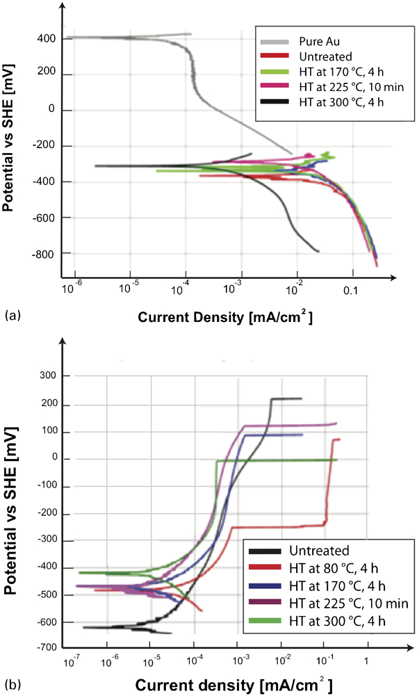
Effect of heat treatment on polarisation curves of a Au–Ti–Al and b Al covered silicon wafer surfaces in 3 mM NaCl
Since Al acts as an anode in the Au–Al galvanic couple, anodic polarisation curves were measured on the Al covered silicon wafer surfaces (Fig. 7b). A negative corrosion potential of −620 mV was measured on the surface of untreated Al covered silicon chips.
The E corr of the Au–Ti–Al covered silicon chips (−350 mV) has a mixed potential between that of Au (410 mV) and Al (−620 mV). Moreover, the influence of Ti cannot be excluded. The effect of annealing on the electrochemical behaviour of the Au–Ti–Al covered silicon chips was analysed. Upon applying a heat treatment at 300°C for 4 h, the following trends were clearly observed:
a slight increase in the E corr from −350 to −300 mV
a clear decrease in the cathodic current density
a decrease in the corrosion current, i corr.
These behaviours can be explained by the interdiffusion of Au and Al and the surface microstructural changes that took place during annealing at 300°C. It is interesting that the cathodic branch of the curves for the untreated and relatively low temperature treated surfaces is similar to that of pure gold, which can be attributed to the relatively high Au concentration of these surfaces.
Evolution of electrochemical events over surface of Au–Ti–Al covered silicon chips: SVET
Mapping of electrochemical events over the surface of the Au–Ti–Al covered silicon chips was carried out under freely corroding conditions in 3 mM NaCl at room temperature. A selected sequence of the SVET maps and optical images are presented in Figs. 8 and 9. Very low current densities were measured over the surface of untreated samples (Fig. 8). After 2 h of immersion in 3 mM NaCl, the active anodic and cathodic events on the surface were not significant and the size and magnitude of the current density did not change. This means that no significant corrosion activity occurred on the surface of untreated Au–Ti–Al covered silicon chips. Similar behaviour was observed for samples heated at 170°C for 4 h.
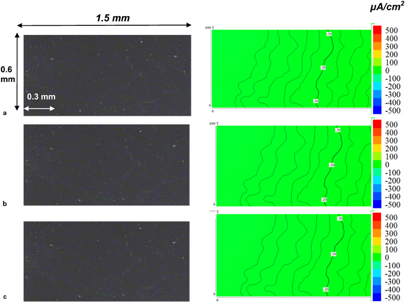
Au–Ti–Al covered silicon chips, untreated: evolution of ionic current arising from surface in 3 mM NaCl
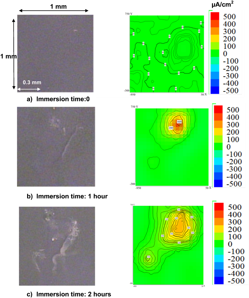
Au–Ti–Al covered silicon chips, annealed at 300°C: effect of heat treatment on ionic current arising from surface in 3 mM NaCl (surface area studied is 1 mm2)
Different features were observed on the samples heated at 300°C for 4 h (Fig. 9). It can be seen that after 1 h of immersion, the cathodic activities of –50 μA cm−2 were balanced by the local anodic activities with a high current density up to 430 μA cm−2. After 2 h of immersion, the anodic areas were enlarged in size.
A high current density of ∼430 μA cm−2 indicates that local corrosion attack takes place after 1 h of immersion. The electrochemically heterogeneous IMCs were most likely the initiators of local corrosion by microgalvanic interaction with the adjacent matrix. After 2 h of immersion, the anodic activities were slightly decreased in magnitude to ∼270 μA cm−2, while the anodic area was enlarged. Corrosion products were seen on the surface after immersion (Fig. 9b and c, left pictures). This further confirms that the heating of the Au–Ti–Al covered silicon chips at 300°C made the surface more susceptible to local corrosion attack.
To summarise, the results clearly show that the annealing at 300°C for 4 h significantly affects the electrochemical behaviour of Au–Ti–Al multilayer thin films and heat treatment at 300°C increases the chances of localised corrosion attack.
The results also indicate that the annealing at 170°C for only 4 h does not significantly affect the electrochemical behaviour of Au–Ti–Al multilayer thin films. However, it is possible that the Ti layer forms a diffusion barrier for Al and Au. Electrochemical behaviour is directly related to the surface structure of the film, which in turn depends on many parameters, such as method of deposition, thickness and integrity of the film, and substrate type. There are studies on growth and morphology of thin Au films, including the effect of annealing.13,14 The authors reported that the surface morphology of Au films on TiO2 was clearly dependent on the Au thickness changing from droplet-like islands (<1·5 nm) to a continuous film (>12 nm). 13 In addition, it was reported that the annealing of Au films on glass increased the area of the individual islands, the island height and the average separation between islands. 14 Previously studied systems were similar to the system presented here. However, some differences were also found. The system presented here was a multilayer system, where an Au layer was applied onto a Ti layer and in turn that Ti layer was applied onto an Al layer. This is different from previously studied systems13,14 where an Au film was applied directly onto a different substrate. In addition, the thickness of Au films studied here is different from that in previous studies (of up to 20 nm). Hence, it is not surprising that some differences in morphology were observed. The droplet-like features and the surface imperfections were observed on the untreated sample of Au–Ti–Al covered silicon wafer surfaces. The surface imperfections can be explained by the porous structure of the Au layer and the thickness of the Ti layer, e.g. the Ti layer of 10 nm is most likely not continuous and hence has local regions where adhesion of Au is poor. These surface imperfections were one of the reasons for the mixed electrochemical corrosion potential E corr of the untreated surface.
Conclusions
The present study demonstrates that the current experimental approach can be used to study electrochemical behaviour of metallic interconnections in microelectronic devices. Local electrochemical techniques, such as MC and SVET, were successfully used to study the corrosion behaviour of wire–bond pad model systems. Au thin films applied on the Ti–Al covered silicon chips were used as a model system to study local electrochemical behaviour of the wire–bond pad interconnection.
A clear link between the surface structure and the electrochemical behaviour was observed. Au layer of 50 nm formed a film with droplet-like features on top. Electrochemical behaviour of the Au–Ti–Al covered silicon chips was studied for the first time using local electrochemical techniques. No significant corrosion activity was measured on the Au–Ti–Al coated surfaces, whether untreated or annealed at 170°C. It is observed that heat treatment of up to 170°C for only 4 h does not influence the electrochemical behaviour and the surface is relatively resistant to general and local corrosion attack.
On the other hand, the electrochemical behaviour of thin Au films was significantly influenced by the underlying materials and the heat treatment at 300°C. Specifically, the corrosion potential and the polarisation behaviour of the Au–Ti–Al covered silicon chips were different from those of pure Au. The electrochemical behaviour was explained by the mixed potential behaviour between Au and Al. An effect of the underlying layers on the electrochemical properties of the Au–Ti–Al covered silicon chips was more pronounced after the heating step. Interdiffusion of Au and Al, as well as formation of relatively Au enriched IMCs, was clearly observed after annealing at 300°C for 4 h. Local pitting was measured on the surface of the Au–Ti–Al covered silicon chips annealed at 300°C when the sample was immersed in 3 mM NaCl.
In conclusion, the current work aims to demonstrate the feasibility and strengths of local electrochemical techniques to study model material combinations for microelectronic applications. For this reason, in this preliminary stage of the research, a relatively simple model system (pure aluminium and pure gold) was selected in order to decrease yet unclear (combined and local) effects of different parameters (such as alloying elements, inclusions, surface contaminations, potential bias, mechanical deformation and temperature) on the local electrochemical response of the Au–Al model system. Follow-up research shall focus on industrially relevant microelectronic assemblies and include, but not be limited to, the analyses of industrially relevant alloyed metal microstructures and metal alloy combinations, surface contaminations, potential bias, mechanical deformation effects as a result of the wire bonding process and operation temperature.