
Abstract
Besides the excellent high-temperature mechanical properties, Si3N4 and SiC based ceramics containing insulating or electrically conductive phase are attractive for their tunable dielectric properties, which may vary from electromagnetic (EM) wave transparent to absorption and shielding. Consequently, SiC, Si3N4, SiON, SiBN, SiBC, SiCN and SiBCN ceramics have attracted extensive interest in recent years. SiO2, Si3N4, Si3N4–SiO2, Si3N4–BN, and Si3N4–SiO2–BN are promising EM wave transparent materials for applications in microelectronic packaging, microwave transparent reaction chamber, radome and antenna window. C, SiC, SiC–C, Si3N4–C and Si3N4–SiC are potential EM wave shielding materials, which can be used as electronic packaging of highly integrated circuits, and be used in wireless communication system, telecommunication base stations and the other electronic devices. Si3N4–SiBC, Si3N4–SiCN and Si3N4–SiBCN are attractive EM wave absorbing materials for potential applications in amplifier, accelerator, microwave heating, anechoic chambers, stealth aircraft and ship. Other potential harsh environment or high-temperature applications will also benefit from the Si–C–N ceramic system. The concept of hybrid structure and EM metamaterials (MMS) opens up new avenues in developing EM wave absorption materials. The key developments and future challenges in this field are summarised. The main issues regarding permittivity of high-temperature structural ceramics are discussed, with an emphasis on the EM wave transparent, shielding and absorbing mechanisms that are responsible for the EM wave properties.
Introduction
High frequency electromagnetic (EM) wave with wavelength varying from 2·4×10−2 to 3·7×10−2 m is used in various environments, especially for critical electronic equipments in wireless communication, medical and aerospace applications, which require EM transparent materials as well as EM shielding and absorbing dielectric materials. These applications include Doppler, weather radar, TV transmission, and telephone microwave relay systems, which work at gigahertz frequencies. 1–6 The commercial wireless communication band was relatively at the early stage of gigahertz range, but the frequency band of newly developed commercial devices has been increased to tens of gigahertz. Therefore, the target frequency range of the above applications is set as 8·2–12·4 GHz (X-band). Recently, EM absorbing properties of magnetic materials, nanomaterials and metamaterials (MMs) have been summarised by Kong et al. 7 EM absorption properties in polymer composites filled with carbonaceous particles have been reviewed by Brosseau et al. 8 Si–B–C–N ceramic has attracted wide attention due to its excellent structural stability, oxidation resistance, creep resistance and high-temperature mechanical properties, etc. The preparation method, microstructure, mechanical, electrical, and optical properties, oxidation resistance, and potential application of Si–B–C–N ceramic have been summarised by Jia et al. 9 The present review will focus on the recent progress in EM properties of Si–C–N based ceramics and composites, which are non-magnetic and thermostructural materials.
When EM wave is incident on a material surface, it experiences three processes: reflection, absorption and transmission, obeying the laws of optics, Fig. 1. When EM wave is incident on the surface of a non-magnetic dielectric material, the electric field induces two different electrical currents within the material, i.e. the conduction and displacement currents, respectively. In dielectric materials, most of the charge carriers are bound and cannot participate in electrical conduction. However, if an external electric field is applied to the material, these bound charges may be displaced. This displacement of charge creates a dipole field that opposes the applied field and the material is polarised. Conduction current is produced by a net flow of free charges, and the bound charges generate a displacement current. Dielectric loss tangent represents tangent of the angle between displacement phasor and total current.
2,3
Electromagnetic properties of a dielectric material are characterised by a complex permittivity ϵ, which can be expressed as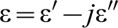
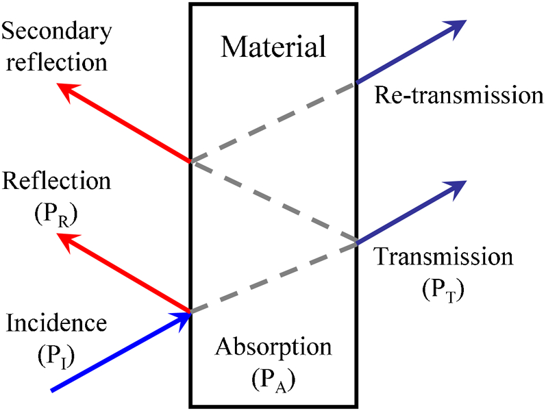
Schematic of an incident electromagnetic (EM) wave through solid material
According to Debye polarisation relaxation equation,
4
the dielectric loss can be evaluated as loss tangent and expressed as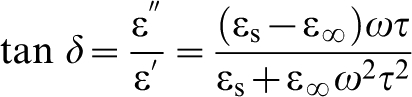
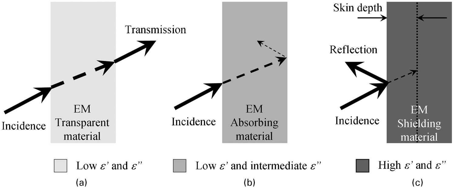
a EM wave transparent materials with low ϵ′ and ϵ″; b EM wave absorption materials with low ϵ′ and intermediate ϵ″; and c EM wave shielding materials with high ϵ′ and high ϵ″
Recently, an interdisciplinary field of numerical studies aiming at EM behaviours of heterostructure mixtures and composites has aroused great attention. The rapidly developing subject of computational EMs in the last decades has been summarised by Brosseau. 11 Computers move the emphasis away from the general theory of macroscopic electromagnetism towards a better look at the detailed features of the randomness and connectedness of heterostructures. It is concluded that computational techniques provide a versatile tool for studying the dielectric properties of complex composite materials and that considerable progress can be achieved by comparing numerical results against analytical predictions for the properties. As the capabilities for performing realistic simulations increase, it might become possible to routinely design on a computer, at least in part, a combination of materials chosen specifically to achieve a desired response to an incident EM wave for a variety of technological and industrial processes ranging from EM transparent to shielding and absorption applications. The EM characterisations of filled polymers, 12 fine-scale particulate composite materials 13 and magnetic field dependence of the effective permittivity 14 have been researched in detail. The numerical study conveniently provides a theoretical basis for microstructure design of EM materials. Table 1 summarises the requirements on dielectric properties of materials for different applications.
Requirements on dielectric properties of materials for different applications in X-band
EM: electromagnetic; PDMS: polydimethylsiloxane.
Electromagnetic transparent materials do not significantly alter the amplitude and phase of EM waves transmitting through them. This type of material is used mainly in the manufacture of antenna housings or radomes, which protect the antennas of radar sets from the effects of the surrounding medium. The transparency of the materials to EM waves is assured by choosing dielectrics with low dielectric loss tangent (tanδ⩽0·01), and relatively low real part of the permittivity (ϵ′ = 1–5), together with suitable electrodynamic design of the material thicknesses. Commercially available radome materials are polymer and fused silica (SiO2), which have low ϵ′ and low ϵ″. For example, ϵ′ and tanδ of polytetrafluoroethylene are 2·1 and 4·2×10−4, while those of fused SiO2 are 3·9 and 3×10⁻⁴.
Electromagnetic interference (EMI) is the disruption of operation of an electronic device when it is in the vicinity of an EM field that is caused by another electronic device, on purpose or not. Electronic enclosures, as well as rooms, vaults and aircraft that house electronics, need to be able to shield EMI. There is an increasing urgency to reduce aircraft weight by using innovative materials (e.g., composite containing carbon fibre) and also provide reliable mechanical properties, combined with the same level of EM shielding provided by comparable metallic alloys. 15 Moreover, it has been revealed that EM wave can promote growth of tumour in human body, 16,17 so it is also necessary to protect human body from EM radiations using shielding materials.
Electromagnetic interference shielding materials refer to the materials that can reflect and/or absorb EM radiation, thereby acting as a shield against the transmission of the radiation through the shield. 18 There is an increasing interest in EMI shielding to protect commercial, defense, and scientific electronic devices and communication instruments. The primary mechanism of EMI shielding is reflection, so the shielding materials must have mobile charge carriers (electrons or holes) that interact with the EM radiations. Metals are the most used materials for EMI shielding. In many instances, a simple metallic foil covering the internal or external surface of the structure is sufficient to reflect the incident EM wave and to preserve the electrical integrity of the system, or to prevent EM wave to escape from the system. 5 The intrinsic wave impedance of free space is equal to 377 Ω, but most metals have an intrinsic impedance of only milliohms, so most of the energy will be reflected when EM wave encounters metals. Similarly, conducting polymers are also good shielding materials against EMI. 19 Owing to the desire for lightweight avionic electronics, laptop computers, aircraft and many other devices, polymer-based composites are increasingly important for EMI shielding, which are also attractive due to their tailorable electrical conductivity, moldability and processability. 20 Polymer-based materials, however, suffer from lower strength as well as limited temperature stability only up to 400°C.
Electromagnetic absorption is a process, in which EM energy is depleted and then transformed into other energy, such as heat energy, so that the wave can not be reflected or permeated through the materials. Absorption is the other mechanism of EMI shielding, and the materials should have dielectric loss by polarization and/or electric loss and/or magnetic loss under the alternating EM field to attenuate the incident EM wave. In a series of applications, absorption of the EM radiation at least from one side of an interface is required: anechoic chambers for testing electronic devices and antennas, or stealth ships and aircrafts for defense operations. Inorganic materials, such as ferrites and metal powders, produce large electric, magnetic and/or dielectric loss, but their intrinsic disadvantages restrict their widespread applications. For example, these materials suffer from high densities (>5·0 g cm−3) and low strength. Generally, they have high electrical conductivity compared with other dielectric ceramic materials, but their permeability decreases rapidly caused by the eddy current loss at high frequency. Thus they are effective only in the megahertz range. Their absorption bandwidth is relatively narrow, and magnetic characteristics are lost above the Curie temperature. Therefore, ferrite and metal powders are usually used as low frequency and low temperature EM absorbers, such as anechoic chambers.
In recent years, polymer-based nanocomposites combining both the high EM loss of nanoparticles and easy processability and multifunctionality of polymers attract great attention as EM absorbers with low density, broad absorption band, high EM loss, and even other functionality, such as anti-causticity and intelligentization. 6 Polymer and its composites have merits such as tunable shielding and absorption response, but they cannot be used for structural applications at high temperatures, due to their poor mechanical properties and lower decomposition temperatures.
Low density ceramics may offer superior effectiveness in the gigahertz frequency range, as well as excellent stability in high-temperature, corrosive and oxidising atmospheres. In the last decade, ceramics and their composites have been demonstrated to have great potential as EM transparent, shielding and absorbing materials, used in various environments.
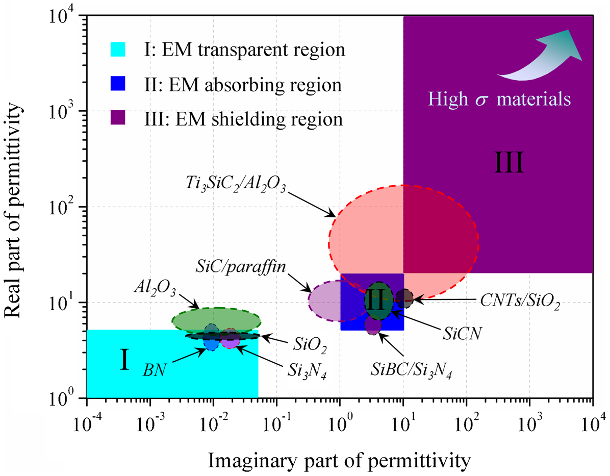
Figure 3 presents EM properties as a function of ϵ′ and ϵ″ of various thermostructural ceramics, such as SiO2, 21,22 BN, 23–28 Si3N4, 29–36 Al2O3, 37,38 SiC, 39–43 SiCN, 44–47 SiBCN, 48,49 Ti3SiC2, 50–56 and carbon. 57–66 Advanced engineering ceramics, such as silicon carbide (SiC) and silicon nitride (Si3N4) are important candidate materials for structural applications, which are attributed to their high thermal and chemical stability, high hardness and strength. SiC is a wide band gap semiconductor which has many practical and potential applications in EM absorption and shielding in harsh environments, while Si3N4 is a promising EM transparent material with small complex permittivity (ϵ′≤ 9). SiCN and SiBCN ceramics based on SiC and Si3N4 offer large possibility to be tailored into EM absorbing and shielding ceramics when the contents of Si, C and N are adjusted.
This article intends to review recent progresses of Si3N4 and SiC based ceramics for EM wave transparent, absorption, and shielding applications, which summarises the approaches to design the ceramics and composites for the corresponding EM applications.
Electromagnetic transparent ceramics and composites
Electromagnetic transparent ceramics and composites have to simultaneously fulfil diverse requirements, like low relative permittivity, good frequency and temperature stability, in a wide frequency range to minimise capacitive coupling and signal delay, along with low dielectric loss to reduce signal attenuation, which are used as microelectronic packaging, radome and antenna materials. For radome materials, bending strength higher than 50 MPa and fracture toughness higher than 1 MPa⋅m1/2 are required.
Principle to design EM transparent ceramics and composites
The relative complex permittivity of an EM transparent material is usually measured by a resonant cavity method. The resonant cavity method is more appropriate for measuring low dielectric loss materials, which has a higher measuring accuracy. 24,35 Electromagnetic transparent materials should have low ϵ′ and low tanδ. The most investigated EM transparent ceramics include amorphous SiO2, hexagonal-BN (h-BN), and α/β-Si3N4.
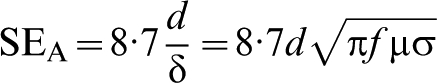
At high frequencies, EM radiation penetrates only the near surface region of an electrical conductor, which is known as the skin effect. The electric field of a plane wave penetrating a conductor drops exponentially with increasing penetration depth into the conductor. The depth at which the field drops to 1/e of the incident value is called as the skin depth δ. The skin depth δ can be calculated by
67,68
The EM transparent materials should have small σ, which is related to ϵ′ and ϵ″. The variation in ϵ′ is attributed to the frequency dependence of the polarisation mechanisms (i.e. electron, atom, and dipole) that contribute to the permittivity. An approach to lower ϵ′ of a dielectric is to reduce the number of polarisable groups per unit volume. The other approach is to form composite using a phase with lower ϵ′. For a statistic mixture, Lichtenecker and Rother developed a logarithmic law of mixing, mathematically expressed as
69


Dielectric loss includes intrinsic and extrinsic loss. The former depends on the crystal structure, which leads to the difference in both ϵ′ and ϵ″ of SiO2, BN and Si3N4. Extrinsic loss is associated with the imperfections in microstructure, e.g. impurities, defects, grain boundaries, porosity, microcracks and random crystallite orientation.
70
Although pores and the secondary phase with low ϵ′ in ceramics can reduce ϵ′, they may also lead to an increase in tanδ
70

Briefly, internal scattering of EM wave in an inherently transparent material may render a material translucent or opaque. Such scattering occurs at defect area within materials, such as density fluctuations, grain boundaries, phase boundaries and pores. In order to attain low ϵ′ and tanδ values, the EM transparent materials should be insulative and may contain micrometre-sized pores and/or secondary phase particle. Compared with micrometre-sized pores and/or secondary phase particle, nano-sized defect and secondary phase have more interfaces, which produce additional dielectric loss under EM field. Therefore, for the EM transparent materials, the relatively large micrometre-sized pores and/or secondary phase are more beneficial to avoid the internal scattering and nano-interface effect.
Microstructure and properties of EM transparent ceramics and composites
Some typical microstructure models of EM transparent ceramics and composites are summarised in Fig. 4.
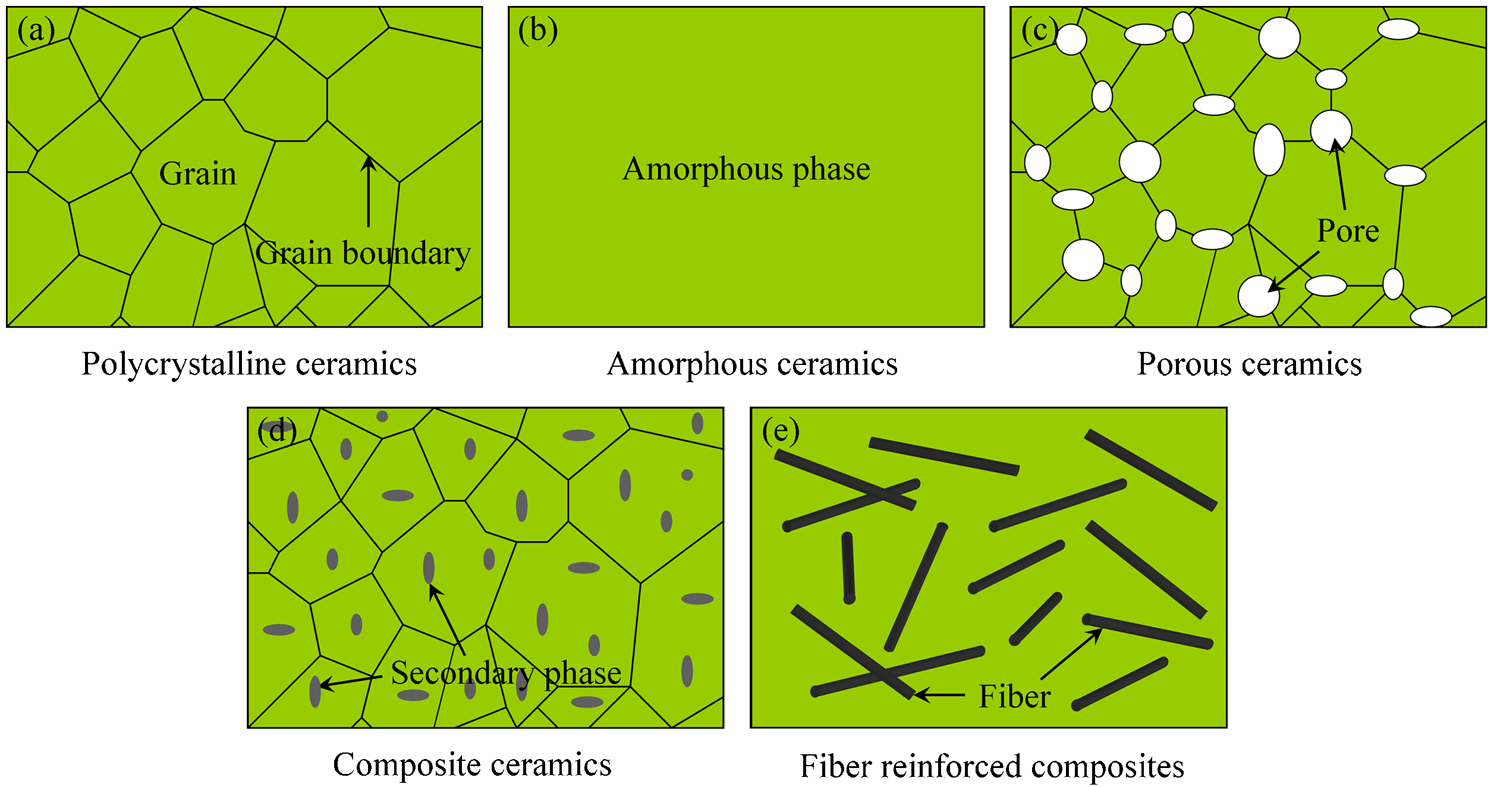
The microstructure models of electromagnetic (EM) transparent materials: a dense polycrystalline ceramic, b amorphous ceramic, c porous ceramic, d composite ceramic, and e ceramic reinforced with fibres
Polycrystalline ceramics
Figure 4a exhibits the microstructure of a dense single-phase polycrystalline ceramics. Dielectric properties of the polycrystalline ceramics depend on its crystal structure and grain size.
Quartz crystal as crystallised SiO2 has electrical conductivity of 5×10⁻¹⁵–10−12 S m−1, with ϵ′ of 4·5–4·6, 71–73 and tanδ of 3×10⁻⁴. 74 Hexagonal-BN and c-BN exhibit ϵ′ of 3·8–5·16 and 7·1. 75 Hexagonal-BN ceramic exhibits an electrical conductivity of <10−13 S m−1 and tanδ of 10−4 at room temperature, a very high sublimation temperature of about 3000°C and good machinability. Though monolithic BN ceramic suffers from low mechanical properties and poor thermal shock resistance, 75 it is commonly used as a radar window material. Incorporation of foreign atoms such as C and O has an influence on the relative permittivity. A real part of the permittivity of as low as 2·2 was achieved for the h-BN polycrystalline film due to the incorporation of carbon atoms into BN films, leading to the formation of B-N, C-N and B-C bonds in the BN film. 75
Compared with SiO2 and BN, Si3N4 ceramics are distinguished by superior mechanical strength, good thermal shock resistance and excellent erosion resistance. Si3N4 is one of the most promising ceramic materials for the applications as EM transparent materials in harsh environments. 76–78 However, its relatively high ϵ′ of 9·0 limits its wide application.
Amorphous ceramics
Resistivity of semiconductors can vary by 10 orders of magnitude between crystalline and amorphous states. It is the changes in short-range order (on the scale of a localised electron), rather than the loss of long-range order alone, that have a profound effect on the properties of amorphous ceramics (Fig. 4b ).
Fused SiO2 has a lower electrical conductivity of 10−16 S m−1 than quartz crystal, with superior dielectric properties and chemical stability, which has been used in radome and window of satellite receiver. Fused SiO2 has a low ϵ′ of 3·9. The introduction of carbon atoms into fused SiO2 forms carbon doped SiO2 with ϵ′ of 2·2–2·7 and SiCOH with ϵ′ of 2·7–3·3. The introduction of F atoms forms fluorosilicate glass (ϵ′ of 3·2–4·0) and fluorinated polyamides (ϵ′ is between 2·5 and 2·9). 79 SiO2 suffers from low toughness (K IC<2MP⋅m1/2), which limits its wide use.
Porous ceramics
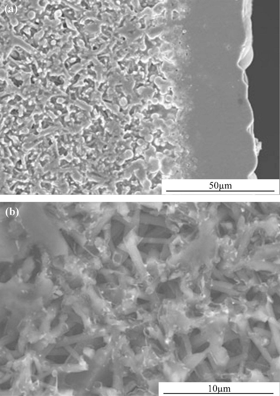
Porous ceramics (Fig. 4c ) are expected to be used for a wide variety of industrial applications ranging from filtration, absorption, catalysts and catalyst supports to lightweight structural components. Carefully tailored microstructure (size, morphology and orientation of grains and pores, etc.) of porous ceramics has led to unique mechanical properties, which cannot be obtained in dense materials. 80–87 Figure 5 exhibits the microstructure of the porous Si3N4 ceramics prepared via low temperature sintering. 77 Fig. 6 summarises the microstructure models of the porous Si3N4 ceramics prepared by freeze casting at different sintering temperatures, and the scanning electronic micrograph (SEM) morphologies of the porous Si3N4 ceramics are shown in Fig. 7. 86
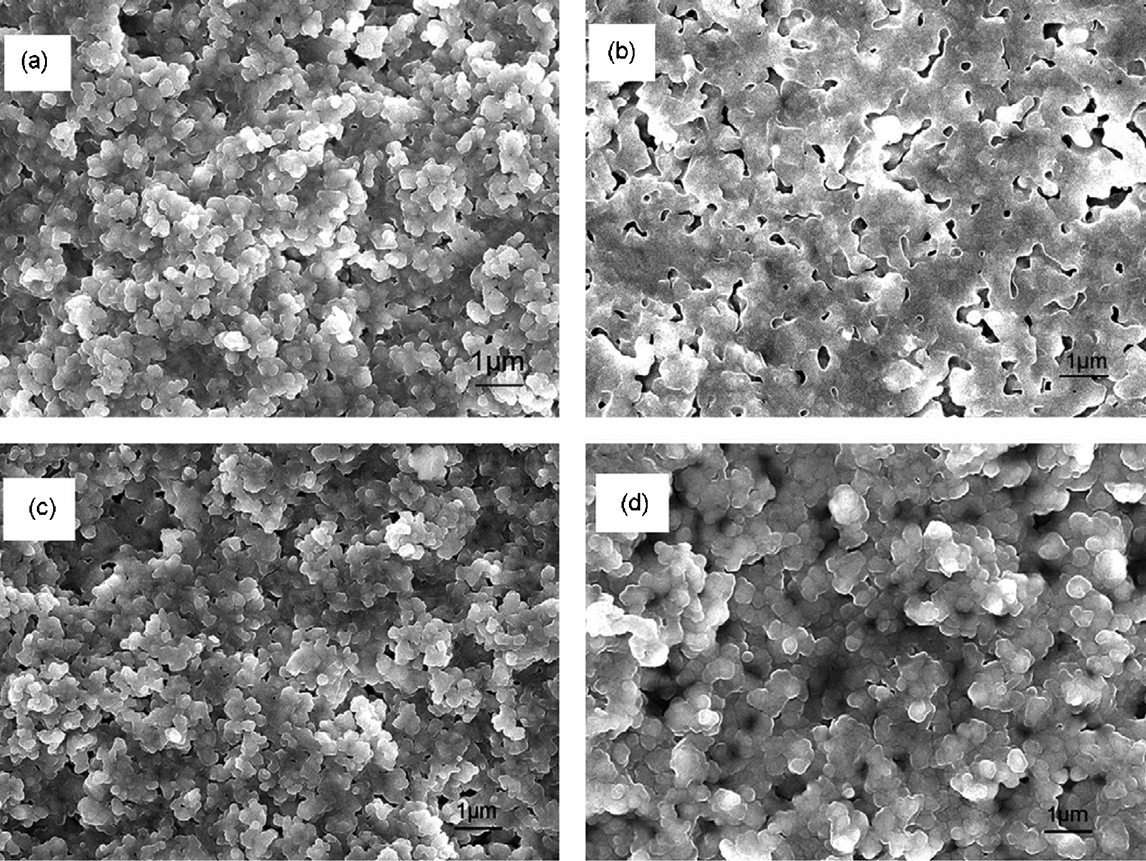
Microstructure of porous Si3N4 at different sintering temperatures with different contents of additives: a 1050°C, 3 wt-%, b 1150°C, 3 wt-%, c 1150°C, 10 wt-%, and d 1150°C, 20 wt-%. 77 Copyright 2009 Elsevier
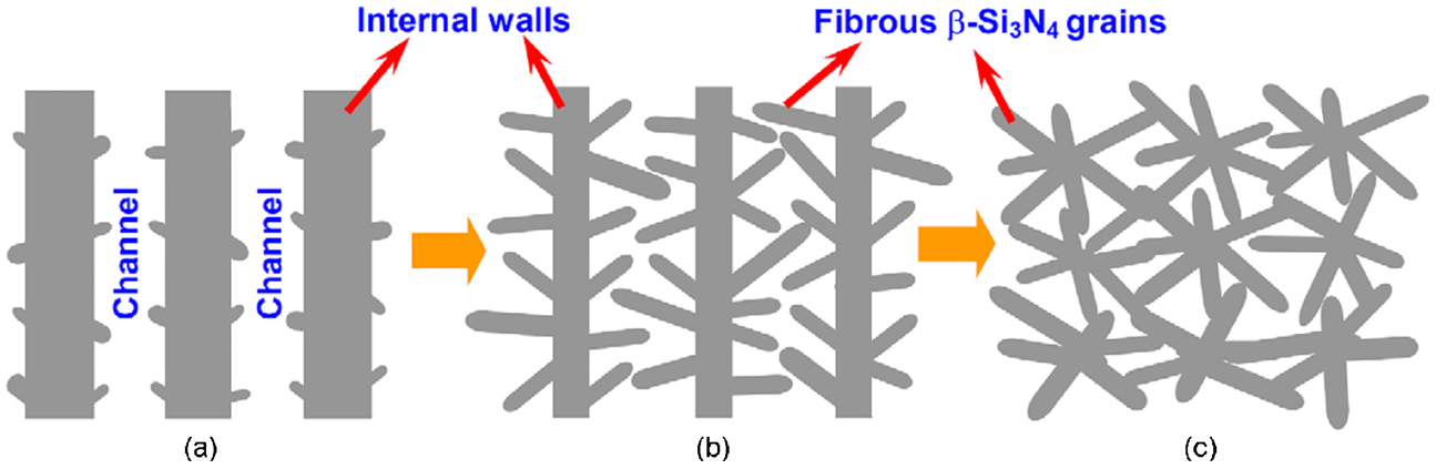
Schematic diagram showing the microstructural development of the porous Si3N4 ceramics sintered at different temperatures: a sintered at 1700°C, showing only small amount of elongated β-Si3N4 grains with low aspect ratio grown from the thick wall of the channels, b sintered at 1800°C, showing a great number of fibrous β-Si3N4 grains grown from the thin internal walls of the aligned pores, and c sintered at 1900°C. The elongated β-Si3N4 grains could grow from one side of the channel to the other side and the aligned channel walls almost disappeared due to the growth of β-Si3N4 grains. 86 Copyright 2010 Elsevier
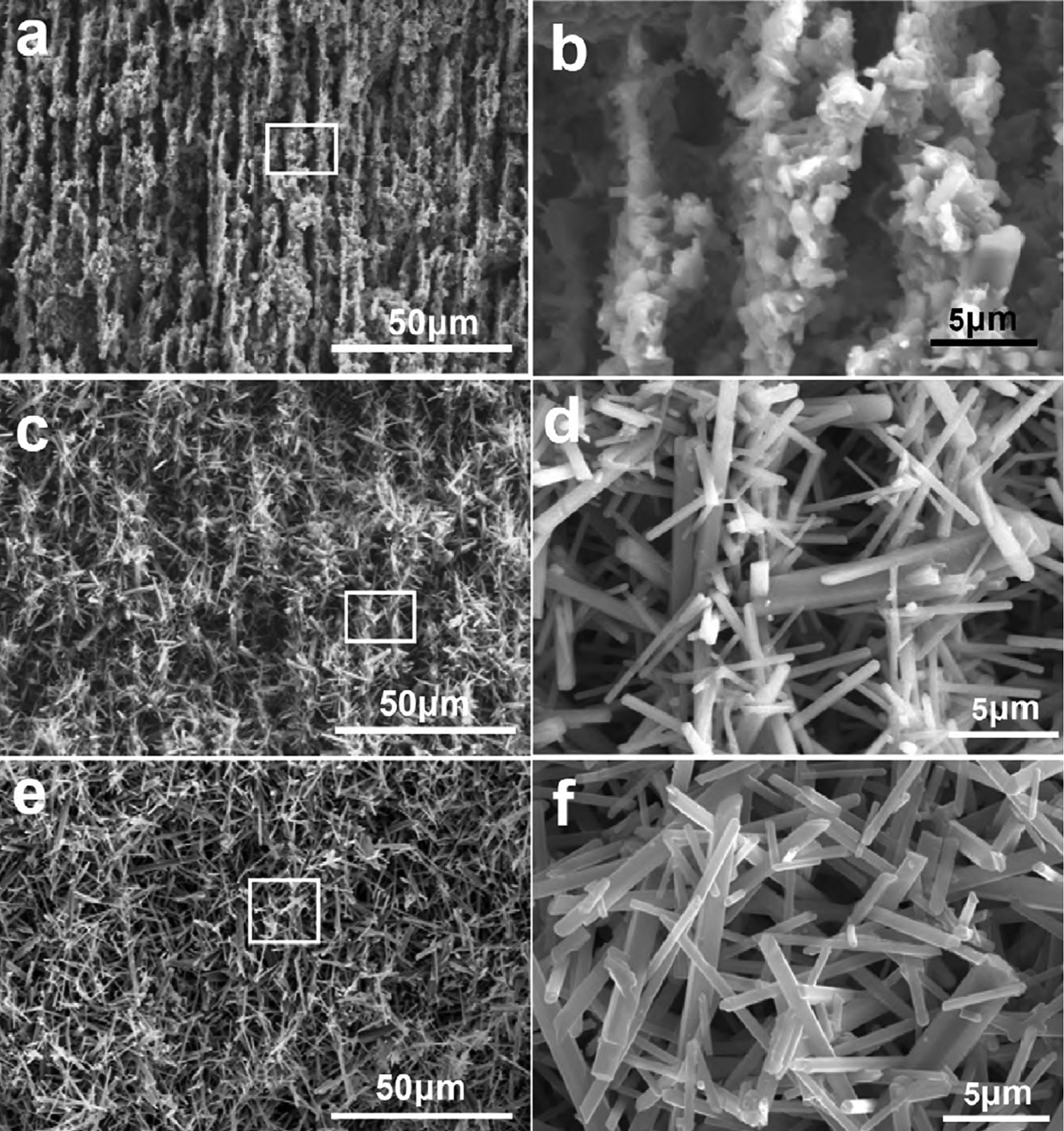
Scanning electronic micrograph (SEM) microstructure of the porous Si3N4 ceramics sintered at a and b 1700°C, c and d 1800°C, and e and f 1900°C. b, d and f the enlarged micrographs of the section marked by white square in a, c and e. 86 Copyright 2010 Elsevier
The SEM morphology of porous Si3N4 using phenolic resin as pore-forming agent is shown in Fig. 8. 88 It has been demonstrated that increasing the porosity is an effective way to lower ϵ′ of ceramics. The ϵ′ of Si3N4 ceramic was remarkably lowered when the porosity reached 35% or above. It seems that the negative effect of porosity on tanδ is not apparent when the pore size is larger than ∼1 μm, which may become dominating when the pore size reaches nanometre scale. When the porosity of porous Si3N4 ceramics increased from 46 to 53% with an average pore size larger than ∼1 μm, ϵ′ decreased from 3·6 to 3·2, and tanδ from 1·4×10−3 to 1·2×10−3, 88 Fig. 9a . The variation of flexural strength and fracture toughness as a function of porosity exhibited the similar tendency, Fig. 9b .
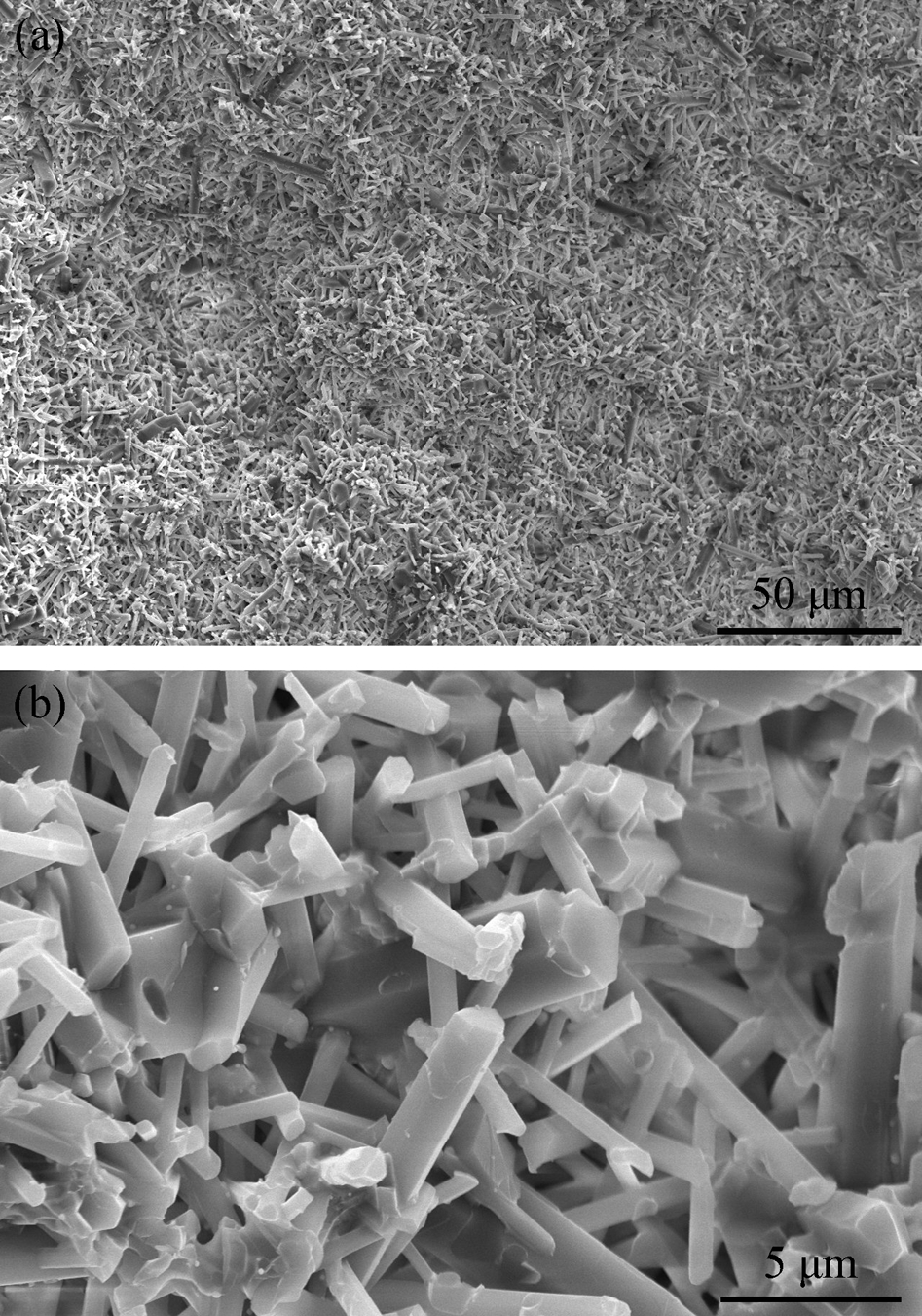
Scanning electronic micrograph (SEM) micrographs of porous Si3N4 ceramics using phenolic resin as pore-forming agent: a low magnification morphology and b high magnification morphology
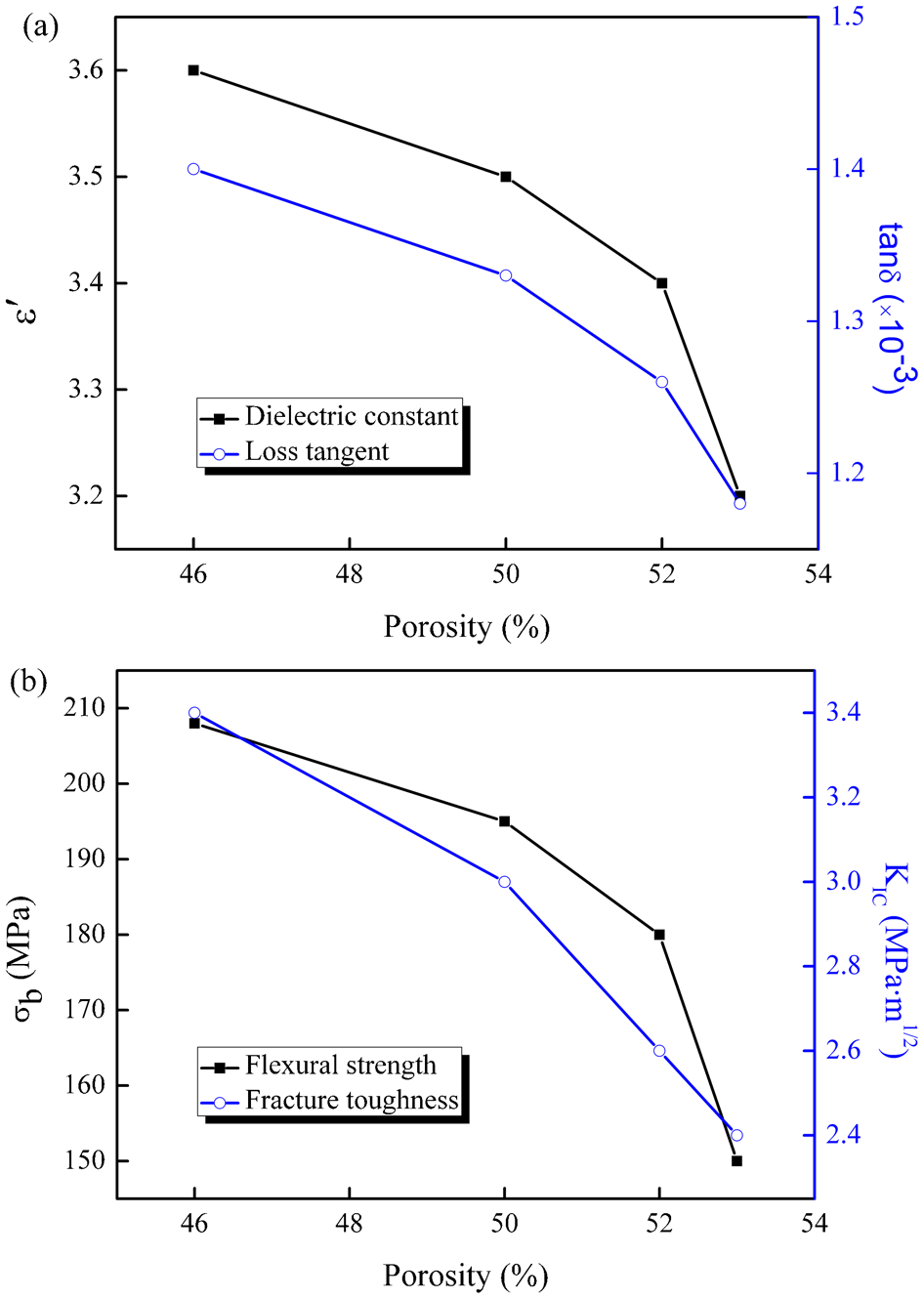
Properties of porous Si3N4 ceramics: a dielectric property and b mechanical property
Composite ceramics
Figure 4d presents the microstructure model of the most researched EM transparent ceramics, which are dense (or porous) polycrystalline (or amorphous) ceramics containing secondary phases. Raising the volume fraction of secondary phase with low ϵ′ to replace pores seems to be an effective way to lower both ϵ′ and tanδ of ceramics without suffering from strength loss. For example, Si3N4 ceramics fabricated from a mixture of 90Si3N4–5MgO–5Al2O3 (wt-%) by pressureless sintering at 1650°C attained a maximum density of 3·16 g cm−3, σb of 500 MPa, ϵ′ of 8·5 and tanδ of 0·003. 89 Furthermore, porous Si3N4/SiON composite ceramics fabricated by silica sol infiltration of aqueous gel-casting prefabricated had significantly lower value of ϵ′ of 4·0–5·0 at 21–39 GHz. 90 Porous Si3N4/SiO2 composite ceramics containing 19·4% porosity fabricated by oxidation sintering had ϵ′ of 4·6 and tanδ of 2·9×10−3. 91 The Si3N4/SiO2 composite ceramics attained improved fracture toughness by micropore crack pinning. 92 The ceramics with a porosity of 23·9% possessed σb of 120 MPa, Vickers hardness (HV) of 4·1 GPa, K 1C of 1·4 MPa m1/2, ϵ′ of 3·80 and tanδ of 3·11×10−3 at 14 GHz.
It should be noticed that a porous Si3N4/BN composite ceramic fabricated by using reaction bonding of silicon nitride (RBSN) technique combined with slip-casting shaping exhibited a ϵ′ of as low as 3·1 due to the high porosity of 53%, with an increased tanδ of ≧4·1×10−3. 93 For the same reason, a dense Si3N4 ceramic attained a high thermal conductivity of 100 W/(m⋅K) and tanδ value as low as 1·4×10−4. 94
In order to improve the mechanical properties, especially the K 1C, of SiO2, 5 wt-% boron nitride nanotubes (BNNTs) were introduced using hot pressing at 1200–1450°C. The BN/SiO2 ceramics had a σb of 121 MPa and K 1C of 1·2 MPa m1/2, which showed low ϵ′ of 4. 95 It seems that increasing nano-grain boundary by combining nano-sized secondary phase may lead to an increase not only in mechanical properties, but also in ϵ′ and especially tanδ, because the nano-grain boundary resulted in considerable attenuation of EM energy. A porous Si3N4 based composite with 10 vol.-% BN nanoparticles (BNnp/Si3N4) was prepared by gas pressure sintering at 1800°C in N2 atmosphere, with ϵ′ and tanδ of 4·31 and 0·006, as well as bending strength (σb) and K 1C of 199 MPa and 3·4 MPa m1/2. 96 Nano-SiO2 and BN were added as secondary phase into Si3N4 ceramics by using gas pressure sintering. σb of the composite ceramics ranged from 75 to 175 MPa, while ϵ′ranged from 3·5 to 4·2 and tanδ varied from 0·5×10−3 to 4·5×10−3. 97 It should be noted that an increasing tendency of the tanδ value was found with increasing content of nano-sized SiO2, but ϵ′ was less influenced. The above results confirmed that the presence of nano-sized grain boundary leads to high attenuation of EM wave.
The dielectric loss of amorphous Si3N4 is lower than that of the crystalline Si3N4. 98 Dielectric properties of porous Si3N4 ceramics combined with amorphous Si3N4, BN and B4C phase by chemical vapour infiltration (CVI) have been researched. 99 After CVI, ϵ′ and tanδ of Si3N4–Si3N4 increased from 3·6 to 4·3 and 2·4×10−3 to 1·5×10−3, those of Si3N4–BN increased to 3·7 and 1·5×10−3 and those of Si3N4–B4C increased to 4·8 and 7·3×10−2.
Fibre reinforced composites
Silica glass fibres and Al2O3-based polycrystalline fibres were employed to reinforce fused SiO2, 76,100,101 Fig. 4e . Silica fibre reinforced silica (SiO2/SiO2) composites exhibit low density, good ablation resistance, excellent dielectric properties, high-temperature stability, fine thermal shock damage resistance and low cost, which are suitable for applications at high temperature in EM environments. 102–106 Continuous fibres, however, may lead to instability of the dielectric properties at high temperatures due to the complex interface between fibre and matrix. Table 2 summarises dielectric properties of SiO2, BN, Si3N4 and their composites. 107–111
Dielectric property of electromagnetic (EM) transparent ceramics
CVI: Chemical vapour infiltration.
Electromagnetic (EM) shielding ceramics and composites
High EMI shielding performances and being lightweight and/or flexible are the important technical requirements for effective and practical EMI shielding applications, especially in areas of aircraft, aerospace, automobiles and fast-growing next-generation flexible electronics such as portable electronics and wearable devices. 112–114 For example, a highly flexible lightweight graphene/polydimethylsiloxane (PDMS) foam composites was fabricated by a novel process, as shown in Fig. 10, which achieved excellent EMI shielding performance. 112 Although advanced ceramics are not flexible, they are lightweight and can work in high-temperature and corrosive environments.
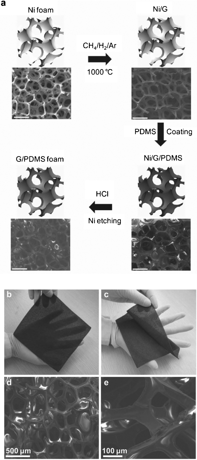
a Schematic of the procedure for fabricating graphene/polydimethylsiloxane (PDMS) foam composites, the scale bars is 500 µm. b, c photographs of a foam composite, showing its high flexibility. d, e scanning electronic micrograph (SEM) images of a foam composite, showing its 3D interconnected network structure. 112 Copyright 2013 John Wiley and Sons
Principle to design EM shielding ceramics and composites
Ceramics for EM shielding should have high ϵ′ and high ϵ″. They usually contain new carbon materials including carbon nanotubes (CNTs) and graphene, which have a high electrical conductivity. It means that carbon/ceramic composites are suitable for EMI shielding. 115
The capability that a material shields EM wave can be expressed by EMI shielding effectiveness or efficiency (SE), indicating how much incident signal is blocked by the shielding material. A SE of 20 dB means that 99% incident signal is blocked, which is required for the commercial applications. 116
Theoretical calculation
According to Schelkunoff's theory,
117,118
the total SE (SET) of a material is determined by the sum of the initial reflection loss (RL) from both surfaces of the materials (loss of energy by first reflection SER), the absorption or penetration loss within the materials (loss of the energy by absorption SEA) and the internal RL at the exiting interface (loss of energy by multiple-reflection SEM):
119,120

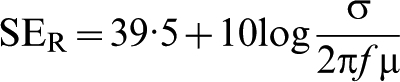
If the shield is thicker than the skin depth, the reflected wave from the internal surface will be absorbed by the conductive material, and thus multiple-reflection can be ignored. However, if the shield is thinner than the skin depth, the influence of multiple-reflection will be significant in decreasing overall EMI shielding. For a far-field plane EM wave, SER, SEA and SEM as a function of frequency f and electric conductivity σ can be expressed as
120–122

Multiple-reflection refers to the reflections at various surfaces or interfaces in the materials, which requires the presence of a large surface area or interface area in the materials. Equation (10) shows that multiple-reflection is a negative term. Therefore, multi-reflection in thin shields reduces the overall SE. When SET>15 dB, equation (7) is usually assumed to take the following form
119

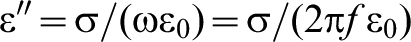
Development of ceramics with high σ is necessary for EMI shielding. ϵ″ is determined by σ in a dielectric material
123,124
Owing to the skin effect, a material having conductive filler (or secondary phase) with a smaller unit size of secondary phase is more effective than the one having conductive filler with a large unit size, 125 which is effective for using the entire cross-section surface of a filler unit for shielding.
There exists a critical volume fraction for the conductive filler in insulator-conductor composite materials, which is known as percolation phenomena. The direct current conductivity (σdc) and ϵ′ versus conducting phase content follow the power law:
126–129


McLachlan et al.
130–132
postulated a generalised effective medium equation for the permittivity of a two-component composite material that combines the effective medium theories (EMT) with percolation scaling law, termed as the two exponent single percolation equation (TESPE). This single equation gives continuous analytical expressions for the real and imaginary parts of the effective permittivity, which can be written as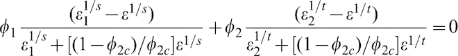
Within the standard percolation theory, it is assumed that s and t are universal descriptors of the critical behaviour, in that they depend only on the geometric dimension, i.e., the most widely accepted values of s and t in 2D percolating networks are s = t = 1·3.
For composites of a dielectric phase randomly dispersed in a continuous matrix of another dielectric phase, Brosseau 133 has demonstrated the use of TESPE to fit the microwave dielectric response of carbon-black filled polymers over a wide range of carbon-black concentrations, and revealed the effects of the surface fraction of the filler and the permittivity contrast between the two phases on the complex effective permittivity of the composite material.
Briefly, for increasing ϵ′ and ϵ″, the EM shielding materials should be conductive, which may partially contain semi-conductive or insulating phases. A ceramic containing small size conductive secondary phase may exhibit good shielding properties only if the content of the secondary phase reaches the percolation threshold.
Measurement method
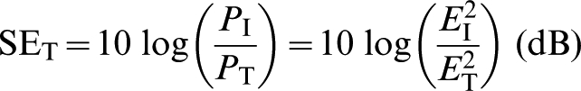
When the SET is measured via experimental route, it can be defined as the ratio between the incident power (P
I) and the transmitted power (P
T) of EM wave
134–136
The commonly used experimental route is wave-guide method, by which SER, SEA and SET can be determined by measuring the scattering parameters (S-parameters). As shown in Fig. 11, S-parameters that correspond to the reflection (S
11 and S
22) and transmission (S
12 and S
21) of a transverse EM wave can be measured using a vector network analyzer (VNA), according to ASTM D5568-08. The reflection coefficient (R) and transmission coefficient (T) are given by 


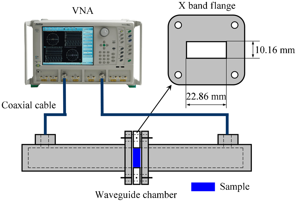
Vector network analyser(VNA) and microwave probe setup for scattering parameter measurements
Generally, an increase in SER represents an enhanced impedance mismatch between the air and the solid material when frequency varies, and SEA scales with increasing attenuation of EM energy in the solid. Therefore, materials with low SER and high SEA are candidate for EM absorption.
Microstructure and properties of EM shielding ceramics and composites
Conductive bulk ceramics
The microstructure model of conductive ceramic material is similar with Fig. 4a . Conductive monolithic materials like metal, graphite and Ti3SiC2, have excellent EMI shielding properties due to their good electrical conductivity. Owing to their higher σ, carbon-based materials are attractive for EMI shielding applications. 137 Carbon fibre and carbon matrix have superior conductive secondary phase and matrix due to their high σ of 2–14×106 and 104–106 S m−1. 137
Recently, Ti3SiC2 ceramics have attracted wide attention due to their unique combination of mechanical, electrical and thermal properties of both metals and ceramics, 138–141 which were used to improve mechanical, 142 electrical, 143 tribological, 144 and environmental properties 145 of ceramics and composites. There were three types of bonding in Ti3SiC2 ceramics, metallic, covalent and ionic, which can make a larger quantity of unpaired defects (i.e. polar centres) to contribute to a higher ϵ′. On the other hand, a high density of electronic states at the Fermi level is responsible for the metal-like conducting properties of Ti3SiC2 ceramics. Both high concentrations of free electrons and electron holes contribute to the enhanced σ of the Ti3SiC2 ceramics (e.g., σ ∼4·5×106 S m−1), which may cause higher ϵ″. 146 As shown in Table 3, ϵ′ and ϵ″ of Ti3SiC2 ceramics were 396 and 585 in X-band, 146 which exhibits a typical metallic character due to the radiation adsorption by sub-bands near the Fermi level. There was high conduction current in Ti3SiC2 ceramics, which led to a SET of 35–54 dB.
Shielding effectiveness or efficiency (SE) of different ceramic materials
CNT: carbon nanotubes; PyC: pyrolytic carbon.
Composite ceramics
The microstructure model of conductive particles reinforced ceramic is similar to Fig. 4d . Composite materials containing conductive secondary phase are more attractive for EM shielding material, which is beneficial to enhance the processability, controllability of conductivity and shielding properties, as well as good mechanical properties. When ceramics have insulating components (SiO2, BN, Si3N4 and Al2O3), which are usually EM transparent materials, with the inclusion of a conducting phase such as graphite, CNT, ordered mesoporous carbon (OMC) and graphene, they are promising for blocking EM radiation and reducing or eliminating EMI. 115,147 Their conductivity and dielectric property can be adjusted and controlled easily through chemical processing.
For OMC filled SiO2 (OMC/SiO2), the percolation threshold was 3·5–5 vol.-%, and absorption dominated shielding was still observed at an OMC volume fraction of 10 vol.-%, 136 leading to a SET of as high as 40 dB. Figure 12 exhibits the high magnification transmission electron microscopy (TEM) images of the OMC/fused silica composite. Incident EM wave entering the OMC/SiO2 composites was reflected and scattered many times between the ordered nanowire arrays of OMC and cannot escape from the limited space until it was completely absorbed, Fig. 13. Thus, the contribution of the absorption to SET of the OMC/SiO2 composites, 35 dB, was much higher than that of SER, 5 dB. When the content of carbon reached 33 vol.-%, the OMC/SiO2 composites attained high electrical conductivity of up to 1·47×103 S m−1, and ϵ″ of 1·5×103. The SET of the sample with a thickness of 2·0 mm was as high as 35 dB with a shielding mechanism dominated by microwave absorption. 148
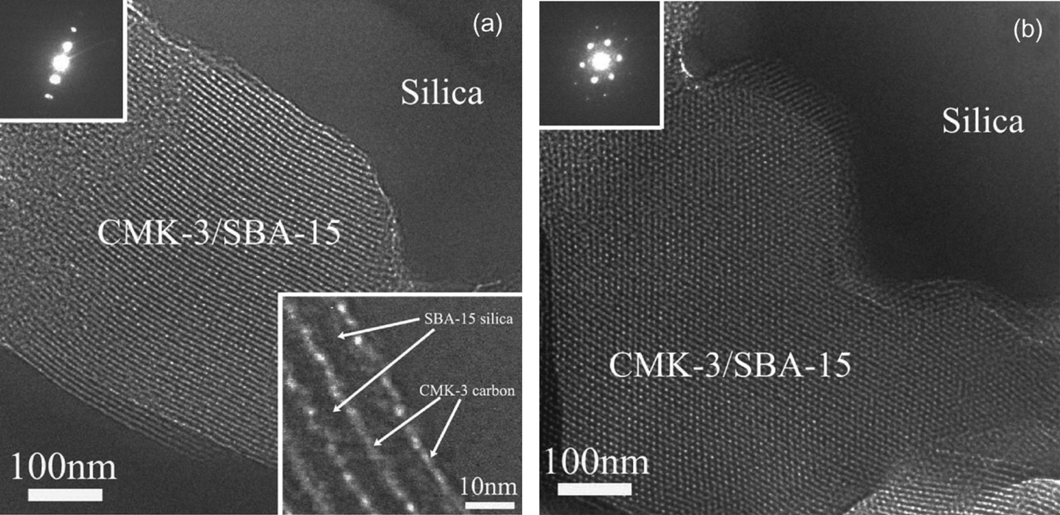
High magnification transmission electron microscopy (TEM) images of the 10 vol.-% ordered mesoporous carbon (OMC)/fused silica composite viewed from a the [100] and b the [001] direction of CMK-3 carbon, respectively. Insets at the upper left of both images show the corresponding selected area electron diffraction (SAED) patterns of the CMK-3/SBA-15 region in each image. The inset at the lower right in a is a high-resolution TEM image of a 136 Copyright 2008 John Wiley and Sons
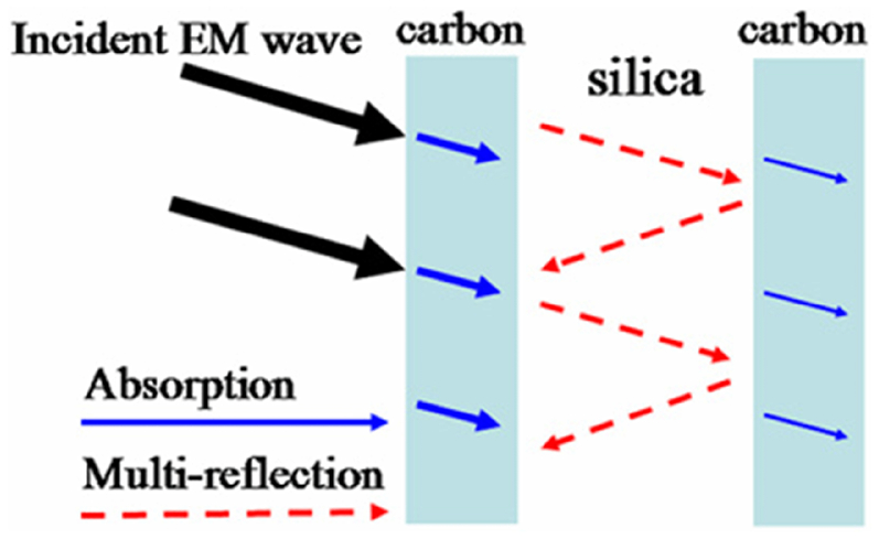
Schematic diagram representing the multi-reflection pathway of incident electromagnetic (EM) wave in the ordered inter-filled string mesostructure of C/SiO2 composite. 148 Copyright 2012 Elsevier
Carbon nanotubes have a much higher σ (>1×10⁵ S m−1) and electrical percolation can be achieved with very low volume fraction of CNTs. It is indicated that, single walled CNTs (SWNTs) with an aspect ratio of ∼5000 (which corresponds to a length of 5 μm and a diameter of ∼1 nm), when dispersed uniformly into a non-conducting polymer, enabled a conducting pathway at a volume fraction of 0·1%. 149 For a CNT-polymer composite, a cross-over from reflection dominated shielding to absorption dominated shielding was observed at a CNT volume fraction of ∼2·3%. 149 It was reported that the critical volume fraction of CNTs in a composite for percolation threshold ranging from 7 to 12%. 56 As shown in Table 3, ϵ′ and ϵ″ reached 38–56 and 31–47, when 10 vol.-% CNT was dispersed in SiO2. Compared with fused SiO2 (Table 2), ϵ″ of CNT-SiO2 was 3×10⁴ times higher than that of SiO2, indicating that CNTs as conductive fillers enhanced σ of SiO2 drastically. As a result, CNT-SiO2 showed a high EMI SET of 28–34 dB in X-band. 136,150
Owing to the high value of σ of graphene and its large aspect ratio, it can be expected that the EMI SE of ceramics containing graphene should be very promising. However, most works focused on the properties of polymer-based materials. A polystyrene-graphene composite exhibited a percolation threshold of 0·1 vol.-% for room temperature σ, which is the lowest reported value for any carbon-based composite except for those with CNTs. 151 Thus, σ of an insulating polymethylmethacrylate (PMMA) filled with graphene reached up to 10 S m−1 at 2·7 vol.-% and 20 S m−1 at 4·2 vol.-% of filler content. 152 A high SE of 30 dB in X-band was obtained for the PMMA composite loaded with 4·2 vol.-% graphene when the sample thickness was 3·4 mm. When Al2O3, which has a low ϵ′ of 7–10, was loaded with 25 vol.-% Ti3SiC2, 56 a SET of 31 dB was observed in X-band.
If the conductive secondary phase is presented as a layer on the matrix grains with larger aspect ratio, the composite material may attain high EMI SE, similar to those containing CNTs and graphene. Pyrolytic carbon (PyC) was infiltrated into Si3N4 ceramics by using precursor infiltration and pyrolysis (PIP) of phenolic resin, leading to a σ of 4·2 S m−1. 153 The SET of porous Si3N4 without PyC was only 2 dB. When the content of PyC in the ceramics reached 4%, a SET of 13–13·5 dB was measured at a sample thickness of 2 mm. Owing to the low content and graphitisation degree of PyC, the ceramics exhibited absorption dominated shielding mechanism with a SER of 3·8–5·7 dB and a SEA of 7·5–8·6 dB. Pyrolytic carbon fabricated by CVI had dense microstructure and high degree of graphitisation. As shown in Fig. 14, PyC was infiltrated into a pressurelessly sintered porous Si3N4 ceramics by using CVI, and dense Si3N4 coating was formed on the surface of the composites using chemical vapour deposition (CVD). Owing to the high σ value of 2·6×104 S m−1, the composites achieved a high SER of 21·0 dB and a SEA of 22·2 dB. Owing to the excellent sealing effect of dense CVD Si3N4 coating, the mean SET of PyC/Si3N4 remained unchanged even after oxidation at 1100°C for 10 h in air. 154
Scanning electronic micrographs (SEM) of the fracture surface of the pyrolytic carbon (PyC)/Si3N4 composite ceramic: a low magnification view and b high magnification view. 154 Copyright 2011 John Wiley and Sons
SiC has lower electrical conductivity than carbon, but SiC ceramics with nano-sized grains can effectively attenuate EM power, leading to the improvement of EM SE. NiO nanorings on the surfaces of SiC powders exhibited enhanced dielectric properties and excellent microwave absorption in the temperature range from 373 to 773 K due to the special ring-like morphology of the NiO nanocrystals, Fig. 15. 39 When nano-sized SiC grains were in situ formed in a porous Si3N4 ceramic using CVI, 44,155 the porous Si3N4–SiC exhibited not only excellent EM SE but also high mechanical properties. 44
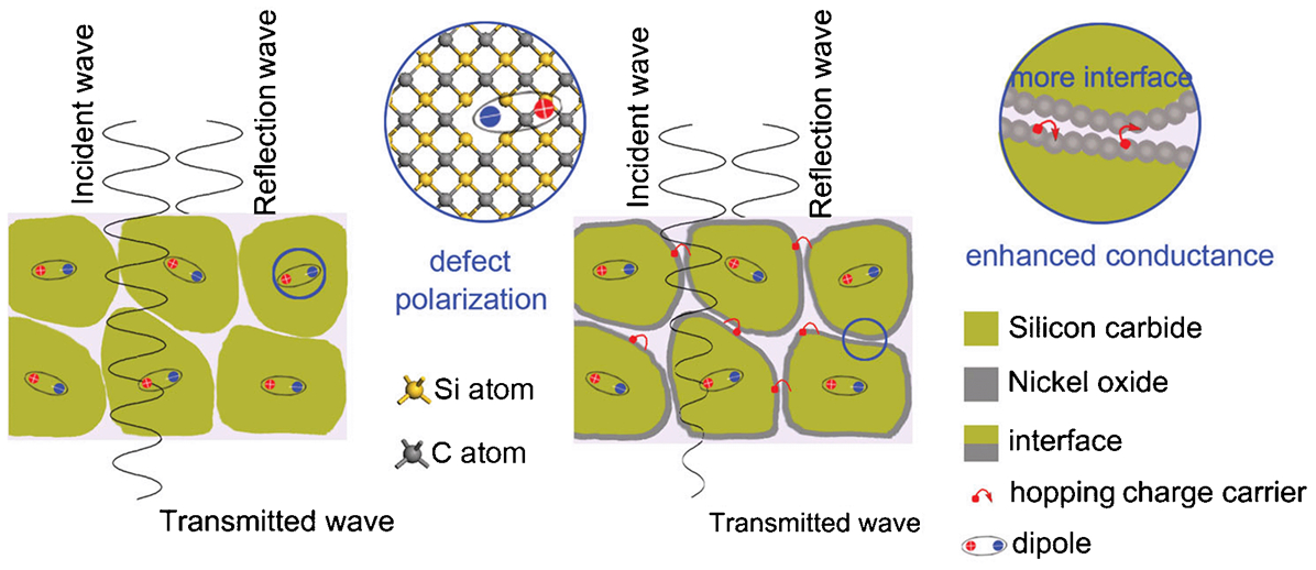
Schematic illustrating the approaches to enhance the microwave absorption of SiC powders 39 Copyright 2013 John Wiley and Sons
Random composite for double negative materials with nickel networks hosted in porous alumina were prepared via wet impregnation, Fig. 16. 156 The plasma oscillation of delocalised electrons in nickel networks led to the negative permittivity. Negative permeability was mainly attributed to the diamagnetic response of current loops in nickel networks. Double negative materials have attracted extensive attention worldwide in recent years and exhibited application potential in electronic, optical and EM wave fields.
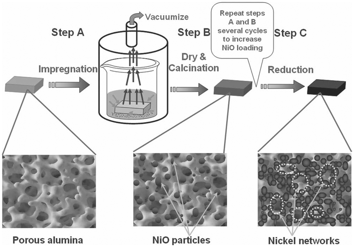
The schematic illustrating the preparation process of Ni/Al2O3 composites. 156 Copyright 2012 John Wiley and Sons
Composites containing fibres
A structural composite that is capable of shielding EMI is particularly needed for aircrafts, which house electronic components. Fibre reinforced carbon and ceramic matrix materials offer not only good high-temperature mechanical properties, but also superior EMI SE.
SiO2 matrix composites containing short carbon fibre (Cfs, σ of 3×10⁴–3·5×104 S m−1) with a diameter of 7 μm and a length of 1 mm achieved a SE greater than 10 dB, Fig. 17. 157 A carbon-matrix composite reinforced with continuous carbon fibres attained an σ of 4·6×104 S m−1, exhibiting an excellent SE of 124 dB, low surface impedance and high reflectivity in the frequency range from 0·3 MHz to 1·5 GHz. 137 The dominant mechanism of carbon-matrix composites containing continuous carbon fibre is reflection.
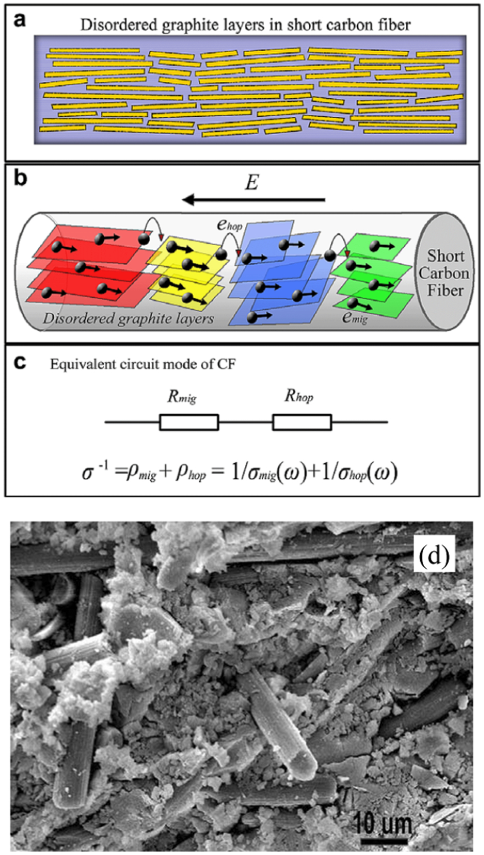
a Schematic illustration showing the microstructure of a CF. b schematic illustration exhibiting the two types of conductance occurring on the graphite layers in a CF. c equivalent circuit model of a CF. d scanning electronic micrograph (SEM) of the CFs randomly dispersed in silica. 157 Copyright 2010 Elsevier
ZrO2-embedded carbon fibres were prepared for use as an EMI shielding material by electrospinning and heat treatment methods, with highest average EMI SE of 31·8 dB in 800–8500 MHz. The EMI shielding effect of the fibres was primarily due to the absorption of EM waves, which prevented secondary EMI by reflection of EM waves. 158
When the conductive secondary phase does not have high σ, it should have much higher aspect ratio in order to achieve high current under EM field. SiC was infiltrated into porous yttria-stabilized zirconia (YSZ) felt using CVI, and a continuous SiC matrix layer was formed around YSZ fibre. When 98 wt-% SiC was introduced into the porous YSZ felt, the mean values of ϵ′ and tanδ were increased from 1·2 and 0·007 to 10·8 and 1·83. The SET was increased from 0·07 dB to 20 dB, exhibiting high surface impedance and low reflectivity over X-band. 159 The dominant mechanism of porous SiC matrix composites containing discontinuous YSZ fibre was absorption.
SiC fibre-reinforced SiC matrix (SiCf/SiC) composites possess superior properties, such as high strength at elevated temperatures, oxidation resistance and microstructural stability under neutron irradiation. The complex permittivity of a SiCf/SiC composite fabricated by using PIP was measured in a temperature range of 25–700°C at frequencies from 8·2 to 18 GHz. 160 Both the real and imaginary part of the complex permittivity increased with temperature.
A continuous PyC interphase made a SiCf/SiC fabricated by CVI exhibit an EMI SE of about 25 dB when thickness of the PyC interphase reached 310 nm (3·3 vol.-%), Fig. 18. 161 Carbon nanotube reinforced carbon fibre/PyC composites were fabricated by PIP method, Fig. 19. 162 With the formation of CNTs, the EMI SE increased from 28·3 to 75·2 dB in X-band. The composite containing 5·0 wt-% CNTs showed SE higher than 70 dB in the whole X-band. Table 3 summarises dielectric and EM shielding properties of typical ceramics.
a 70 nm, b 120 nm, c 180 nm, d 250 nm, and e 310 nm. 161 Copyright 2013 Elsevier
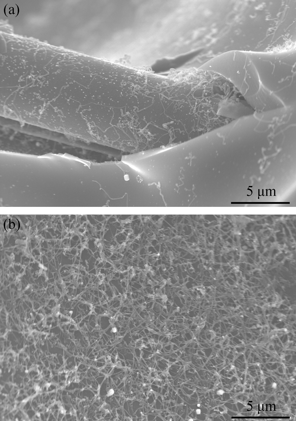
a segregated pyrolytic carbon (PyC) matrix and carbon fibre were bridged by CNTs, and b high magnification morphologies of CNTs. 162 Copyright 2014 Elsevier
Electromagnetic absorption properties of ceramics and composites
The development of EM absorbing materials originated from EMI shielding applications. For example, Cm/SiO2, Cf/SiO2, PyC/Si3N4, SiC/ZrO2 and SiC/Si3N4 are applied to EM shielding with high absorption. Electromagnetic absorbing materials are expected to have broad bandwidth, minimum RL, and small thickness or be lightweight. 7,163–172 A high EM absorption implies minimised transmission and reflection.
Principle to design EM absorption ceramics and composites
The capability of a material to attenuate EM is expressed by the absorption capacity or absorption coefficient A, defined as the ratio between absorbed power P
A and incident power P
I when the EM wave transmits out the materials, i.e. A = P
A
/P
I = 1−|S
11
|
2−|S
21
|
2.
19,157
A/d means absorption coefficient per millimetre. The EMI shielding reflection coefficient R, absorption coefficient A and transmission coefficient T can be calculated. R and T are primarily given as R = |S
11
|
2 and T = |S
21
|
2. Authors can use the relation A+R+T = 1 to obtain A. In addition to the material thickness, A depends on the effective relative permittivity and effective σ of the material or system. When the sample is tested in a wave-guide chamber,
173
the value of A as a function of permittivity can be also expressed as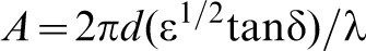
In order to eliminate the transmission of EM through an absorbing material and derive the absorption properties by analysing the reflection of the wave, the United States Naval Research Laboratory (NRL) arch free-space measurement method is used to measure the reflected power of the materials placed on a metal panel, Fig. 20. The EM absorbing property of the materials is evaluated with reflection coefficient (RC) or RL or reflectivity, which can be expressed as
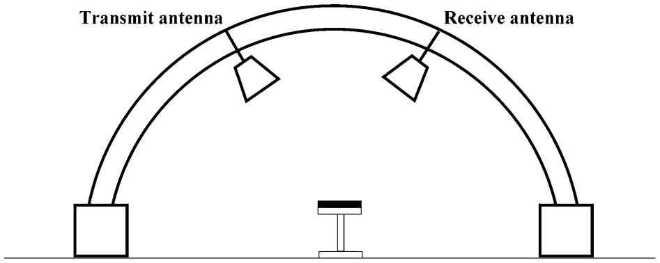
Schematic of Naval Research Laboratory (NRL) arch reflectivity test setup
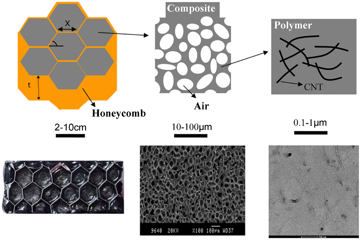
Electromagnetic absorbing materials should meet the following requirements: first, the characteristic impedance of materials should be as close to the impedance of free space as possible; second, the incident EM wave can enter absorbing materials, in which the EM wave is attenuated rapidly. It has been shown that the best absorption of the materials with a sample thickness of 10 mm is attained when ϵ′ is close to 1 and σ is around 1 S m−1 at 10 GHz, 5,174 which can be achieved by designing a hierarchical structure of honeycomb filled with CNT-polymer porous hybrid material, Fig. 21. 5
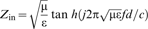
Based on the transmission-line theory and metal back-panel model,
175
RC can be determined from relative complex permeability and permittivity
RC as a function of ϵ′ and ϵ″ is exhibited in Fig. 22. At a frequency of 10 GHz and a sample thickness of 2·86 mm, the optimum ϵ′ and ϵ″ are equal to 7·3 and 3·3 to get the minimum RC, Fig. 22a . Figure 22b presents the top view of Fig. 22a . 176
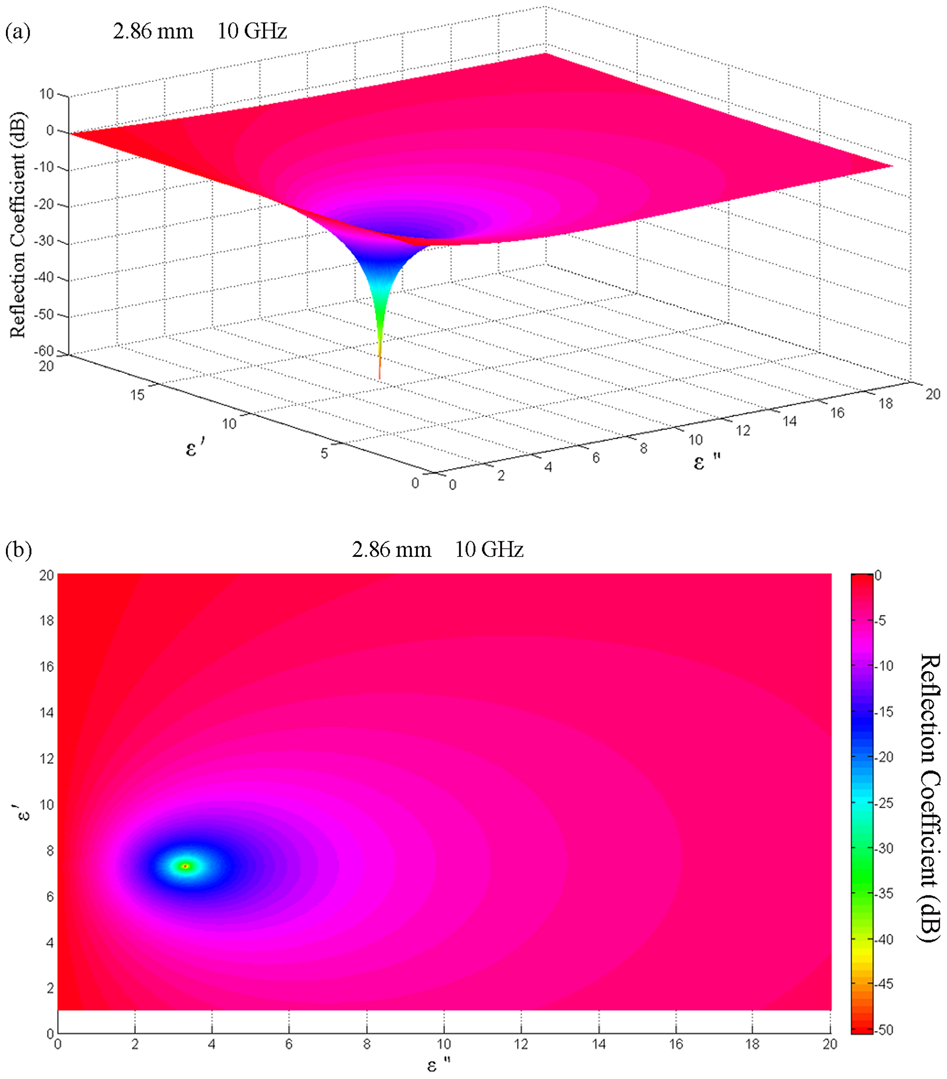
The relationship between permittivity and reflection coefficient: a three-dimensional view, b top view of a. 176 Copyright 2013 US, the USA Chemical Society
When the thickness of the EM absorbing materials is the odd multiple of a quarter-wavelength, a sharp destructive interference takes place. This is caused by the inverse phase angle of the reflection EM wave from the upper and bottom surfaces. When the EM absorbing materials are thick enough, the RC tends to be a stable value.
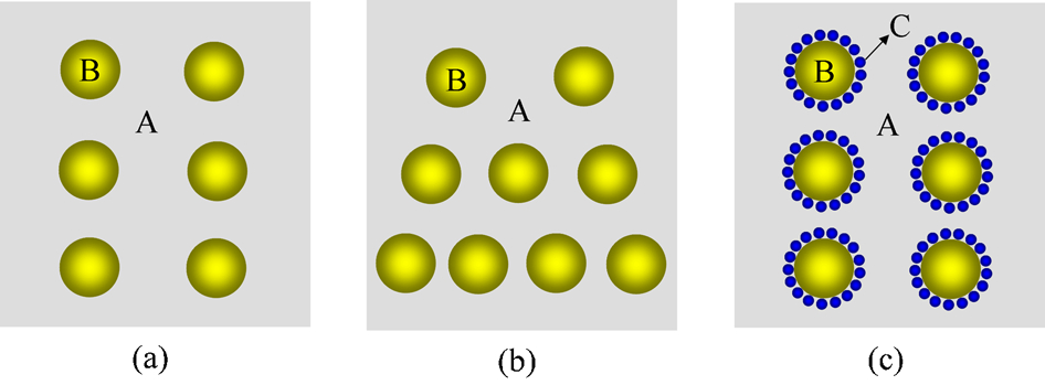
For optimising ϵ′ and ϵ″, EM absorption materials are composed of an electrically insulating matrix, denoted as A phase, an electrically lossy phase denoted as B phase, and sometimes an intermediate phase denoted as C phase. 176 The EM absorbing materials should contain part of the following components: nano-sized pores, nano-sized secondary phase, conductive/semi-conductive secondary phase and insulating matrix.
Microstructure and properties of EM absorbing ceramics and composites
The typical microstructure models are exhibited in Fig. 23.
a A/B type; b gradient A/B type; c A/B/C type
A/B type ceramics and composites
For a conductive or semi-conductive materials (the B phase), pores may act as A phase, Fig. 23a . The coupling of porosity with electrical conductivity and dielectric properties in the same element will lead to more versatile components with an even wider set of properties, for applications of EM absorption. 177,178 Therefore, SiC foam and SiC woven fabrics exhibited attractive EM absorption properties. 179,180
Si3N4 bonded porous SiC ceramics were fabricated by the combination of freeze casting and carbothermal reduction reactions, Fig. 24. 181 Si3N4 bonded porous SiC attained flexural strength of 164·3 MPa at 33% porosity and 80·5 MPa at 46% porosity, whose linear shrinkages were only 1·06 and 1·94%. The superior properties and porous microstructure make it possible for a potential application in EM absorption field.
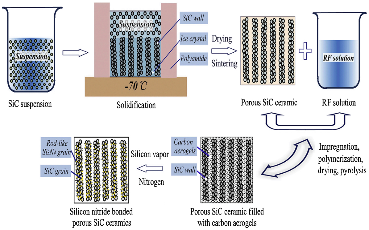
Scheme of the processing routes used for the fabrication of porous SiC ceramics. 181 Copyright 2013 Elsevier
Porous SiC/Al2O3 composites were fabricated by using an infusion method of incorporating SiC polymer precursor into porous alumina substrate. Porous SiC/Al2O3 composites exhibited a controllable variation in complex dielectric permittivity as a function of frequency over the range of 0·001–18 GHz. When the content of SiC reached 17 wt-%, ϵ′ ranged from 9 to 12, and ϵ″ from 2·5 to 6. 182
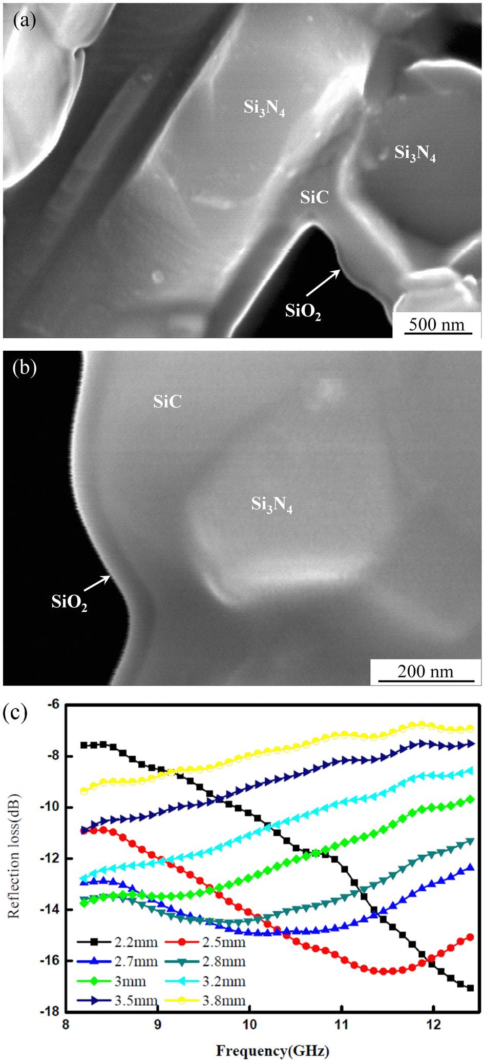
Porous Si3N4–SiC composite ceramics were fabricated by CVI with porous Si3N4 ceramic as preform. The grain size of SiC was 25–30 nm. Average ϵ′ of the Si3N4–SiC increased from 3·7 to 14·9 and ϵ″ increased from 0·017 to 13·4, when the content of SiC increased from 0 to 10 vol.-%. The Si3N4–SiC ceramics with 3 vol.-% SiC showed a RC below −10 dB (90% absorption) at 8·6–11·4 GHz, with the minimum value of −27·1 dB at 9·8 GHz, when the sample thickness was 2·5 mm. 183 The excellent EM absorbing capabilities of the Si3N4–SiC ceramics were attributed to the interfacial polarisation at the interfaces between Si3N4 and SiC and at grain boundaries between SiC nanocrystals.
Si3N4–SiBC composite ceramics were fabricated by infiltrating SiBC into porous Si3N4 ceramic using CVI. Si3N4–SiBC composite ceramic showed not only excellent EM absorbing property, with a minimal RC of −28 dB, but also superior mechanical properties, with a flexural strength of 260 MPa. The excellent wave absorbing property was attributed to the unique microstructure of the CVI SiBC. 49
Owing to the formation of continuous SiC matrix layer composed of SiC nanocrystals in the porous YSZ felt by CVI, as shown in Fig. 25a , which was beneficial for the production of induced electrical current and the enhancement of dielectric loss, the porous SiC/ZrO2 composites attained not only good EM shielding properties but also absorption properties. RC of the SiC/ZrO2 composites with a thickness of 5 mm at 8–18 GHz was smaller than −6·5 dB, and the bandwidth below −10 dB was 5 GHz at room temperature, which increased to 5·9 GHz at 800°C (Fig. 25b ). 159
Morphology and RC of SiC/ZrO2 composites: a scanning electronic micrograph (SEM) photo; b RC as a function of frequency at different measurement temperature using arc free space method at a sample dimensions of 180×180×5 mm3. 159 Copyright 2012 Elsevier
Similar to pores, SiO2 and/or BaSi2Al2O8 can also act as an A phase. Carbon fibre reinforced dense BaSi2Al2O8 glass-ceramic matrix composite (Cf/BaSi2Al2O8) with the similar microstructure were fabricated by hot-pressing technique. 184 For carbon fibre reinforced SiO2 matrix composite (Cf/SiO2), a RC ranging from −8·7 to −10·2 dB in X-band and an absorbing coefficient of 0·1 per unit millimetres were reported, which scaled up with increasing testing temperature up to 600°C. 157 Cagelike ZnO/SiO2 composite ceramics containing 20 wt-% ZnO attained a minimum RC of −10·7 dB at 12·8 GHz. 166 The absorption bandwidth with a RC lower than −10 dB was about 0·5 GHz.
SiC nanowires reinforced SiOC ceramics were fabricated through in situ growth of SiC nanowires in SiOC ceramics by pyrolysis of polysiloxane. 185 SiC nanowires were formed in situ by the addition of ferrocene. Owing to the formation of SiC nanowires in the inter-particle pores of SiOC ceramics, the SiOC particles were bridged, which led to the increase of electrical conductivity, Fig. 26. With the increase of SiC nanowire content, the RC decreased from −1·2 to −20·0 dB.
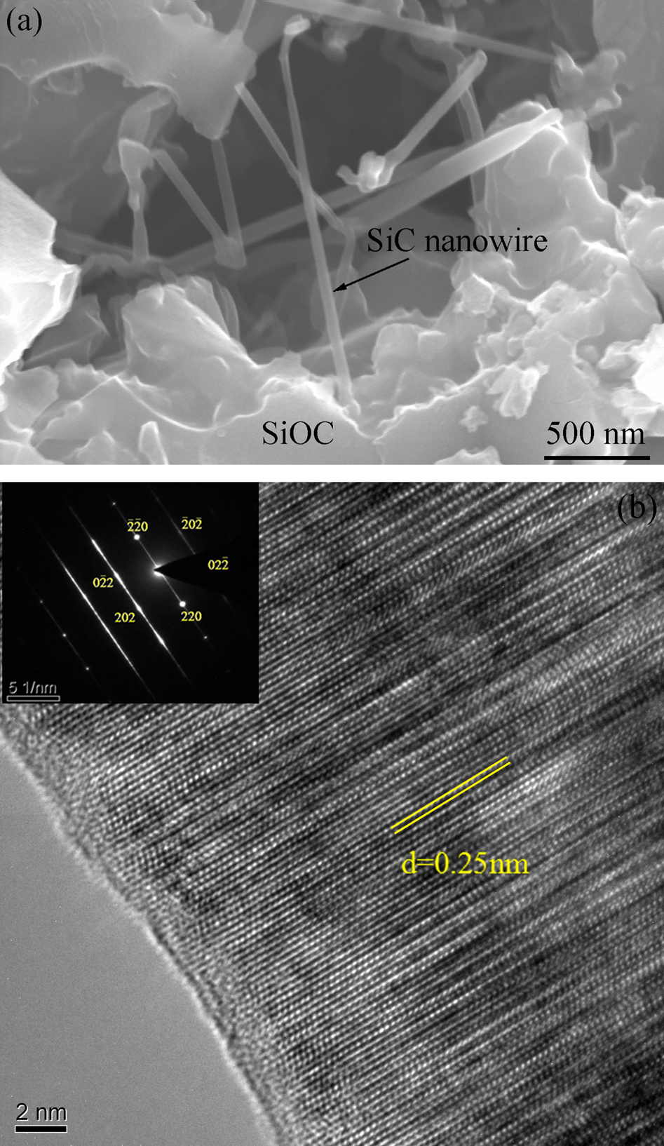
a Scanning electronic micrograph (SEM) micrographs of SiC nanowires reinforced SiOC ceramic, b HR transmission electron microscopy (TEM) micrographs of SiC nanowires
In a similar case, Al-doped ZnO particles were infiltrated into porous ZrSiO4 substrates to form an Al-doped ZnO/ZrSiO4 composite ceramics by using a sol-gel process. The doping of aluminium resulted in the high-concentration carriers, leading to an improvement in polarisation capability and electric conductivity. 186 Consequently, the Al-doped ZnO/ZrSiO4 composite ceramics exhibited excellent EM absorbing properties at temperatures upto 500°C. 187
A Si3N4–SiC/SiO2 ceramic was fabricated by oxidation of Si3N4–SiC ceramics at 1100°C for 10 h in air (Fig. 27a ). The composite ceramic attained a multi-shell microstructure (Fig. 27b ) and exhibited reduced impedance mismatch, leading to excellent EM absorbing properties. When the sample thickness was 3·5 mm, RL of the Si3N4–SiC/SiO2 was lower than −10 dB (>90% absorption) in the frequency range of 8·3–12·4 GHz, with an effective absorption bandwidth of 4·1 GHz. 155 When the sample thickness was 2·5–3 mm, RL of the Si3N4–SiC/SiO2 was lower than −10 dB over the whole X-band at 700°C, Fig. 27c .
a low magnification scanning electronic micrograph (SEM) micrograph, b high magnification SEM micrograph, c RC as a function of frequency at different sample thickness measured at 700°C. 155 Copyright 2013 Elsevier
Constructing graphene-based heterostructures by rational designation is an efficient strategy to attenuate EM wave energy. G/Fe nanohybrids, G/polyaniline nanorod arrays, G/Fe3O4@Fe/ZnO quaternary nanocomposites and G/Fe3O4 were designed and synthesised recently. 188–191 Compared with other magnetic materials and graphene, the nanocomposites exhibited significantly enhanced EM absorption properties.
Effective resistivity and complex permittivity of two series of MWCNT reinforced polymer were measured with a wide range of loadings. 192 The electrical and microwave relaxational behaviours of the MWCNTs/polystyrene latex samples were different from the MWCNTs/epoxy ones because these samples exhibited different filler mesostructures. A novel microwire/CNT/rubber multiscale composite is reported. 193 Compared to the composites containing only CNTs, the hybrid composite showed enhanced conductivity and permittivity and decreased intrinsic impedance, leading to significant improvement of absorption yet along with the increase of RL.
When Ti3SiC2 powders were uniformly dispersed in paraffin, the effective absorbing bandwidth (below −10 dB) of the composite containing 70 wt-% Ti3SiC2 was almost over the whole X-band and the lowest RL was −33·8 dB. 52
Gradient ceramics and composites
When B phase is distributed in A phase with a gradually increasing content (Fig. 23b ), the intrinsic impedance of the surface of the material (A phase) is close to the impedance of free space, and the incident EM wave can enter the materials, which is attenuated gradually through the gradually distributed B phase.
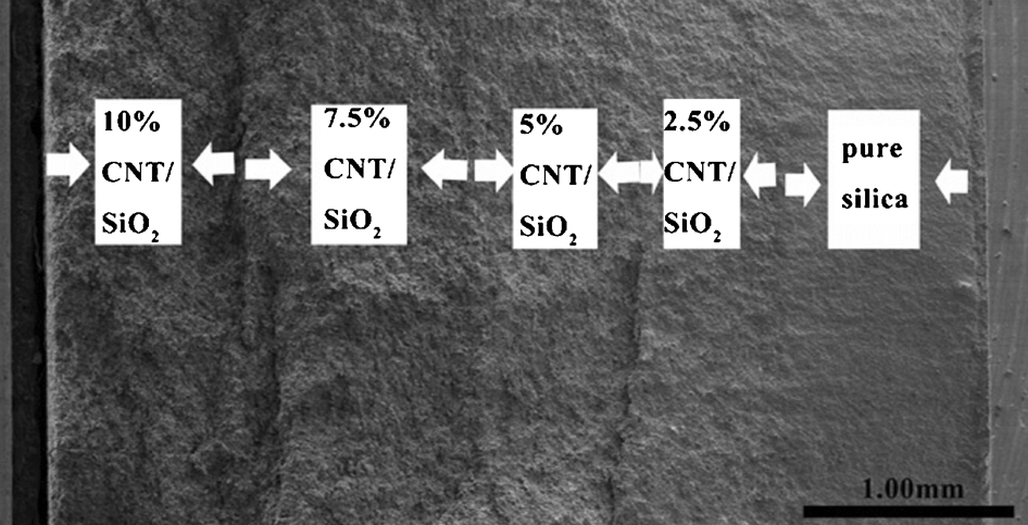
A novel multilayered CNT/SiO2 composite was fabricated by using hot-pressing sintering, Fig. 28. 194 A gradient layered structure was designed to improve its absorbing properties. The gradient CNT/SiO2 composite was shaped by adding five groups of mixed powders with different CNT contents (0, 2·5, 5, 7·5 and 10 wt-%). The results showed that the gradient CNT/SiO2 had a better absorbing capability, which was 1·5 times higher than that of the normal CNT/SiO2. 194
Scanning electronic micrograph (SEM) image of the fracture surface of multilayered material. 194 Copyright 2011 Elsevier
Pyrolytic carbon-Si3N4 ceramics with gradient PyC distribution (Gradient-PyC–Si3N4) was fabricated by using directional oxidation. After directional oxidation for 1·0 h, the EM absorptivity of the gradient-PyC–Si3N4 was increased significantly from 0·8 to 50·1% with an obvious reduction of EM reflectivity from 99·2 to 43·8%. 195
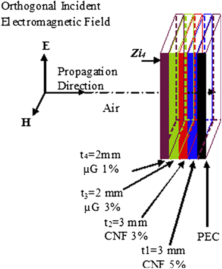
A multilayer gradient polymer-matrix composite was designed, which contained 1 wt-% graphite in the first layer, 3 wt-% graphite in the second layer, 3 wt-% carbon nanofibres (CNFs) in the third layer and 5 wt-% CNFs in the fourth layer. The results obtained showed that over the most part of bandwidth the reflection coefficient had a value lower than −20 dB, with two peaks below −35 dB. Figure 29 exhibits the schematic diagram of four layer radar absorbing material structure. 196
Four layer radar absorbing material structure. 196 Copyright 2010 Elsevier
A/B/C type composite ceramics
When the third phase C, which has larger ϵ′ and ϵ″ than A phase, but has smaller ones than B phase, is added into the EM absorbing materials composed of A and B phases, the A/B/C type composite materials may achieve an increased tanδ but attain a lower ϵ′.
When B phase is surrounded by nanoparticles of C phase (Fig. 23c ), the hybrid materials have more interface than the one that B phase is coated by a layer of C phase, so that better interfacial polarisation capability can be obtained. The introduction of nano-sized C phase with intermediate permittivity into A/B type dielectric material can produce more grain interface, which results in an increase in dielectric loss.
If C phase is a nano-sized pore, the effect of volume fraction of C phase on dielectric loss of dielectric materials is shown in equation (6). Nano-grain interfaces have a high density of point defects and dangling bonds, which may be three orders of magnitude higher than the ones in most composite with the conventionally sized particles. Defects can act as polarisation centres, which will generate polarisation relaxation under the alternating EM field and absorb the EM wave.
Owing to the lower ϵ′ and higher tanδ, the graphite/nano SiC/paraffin composites with a thickness of 2·96 mm achieved a RC below −10 dB at 9·8–15·8 GHz. 197
Results on ZnO/ZnAl2O4/paraffin composite confirmed the great potential of A/B/C type materials. Submicron-sized ZnO particles were dispersed in ZnAl2O4 nanoparticles, Fig. 30, in which the elongated interface area exhibited enhanced EM absorption capability. 176 Consequently, it is reasonable that the ZnO/ZnAl2O4/paraffin composite possessed excellent EM absorption properties. 176 Absorption coefficient per unit thickness increased from 0·01 to 0·13 mm−1, compared with the A/B type materials. The minimum reflection coefficient reached −25 dB and the effective absorption bandwidth covered the whole X-band.
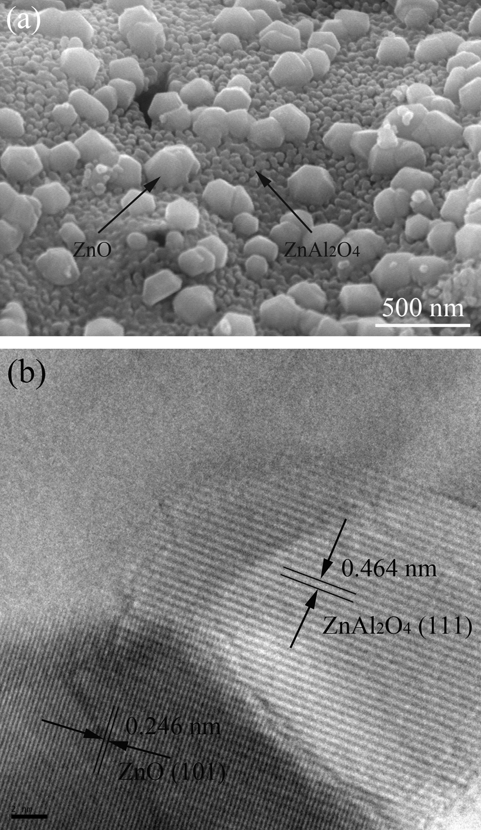
Morphology of ZnO/ZnAl2O3 absorbers: a scanning electronic micrograph (SEM), b transmission electron microscopy (TEM). 176 Copyright 2013 US, the USA Chemical Society
Hybrid structure
By tailoring the phase composition and microstructure of the materials, the properties can be further optimised by designing a hybrid structure. A rectangular pattern of conductive polymer (CP) paste was designed and printed on a glass/epoxy composite substrate. 198 The unit cell of rectangular CP was 6×6 mm2, and the patterned layer was inserted between the two glass/epoxy composite layer. Total thickness of EM wave absorbing structure was about 3·9 mm, and more than 90% absorption was confirmed over the whole X-band.
The hierarchical architecture involving the metallic honeycomb and CNT-filled polymer foam shown in Fig. 21 enlarged the potential to tailor the EM absorbing properties of A/B/C type materials. 5 The waveguide characteristics of the honeycomb, combined with the conductive nanocomposite foam, reduced the real part of the effective relative permittivity of the hybrid, resulting in very high EM absorption in the gigahertz range, superior to any known material. However, similar hybrid structure composed of ceramic and ceramic based composites has not been reported.
Electromagnetic MMs
A special case of hybrid structure is MMs. Metamaterials are often defined as the structures of metallic and/or dielectric elements, periodically arranged in three or two dimensions. Related structures were known as artificial dielectrics or EM materials, which show their peculiar responses to EM wave. 199–201
As an effective medium, MMs can be characterised by a complex electric permittivity: ϵ = ϵ′−jϵ″ and magnetic permeability μ = μ′−jμ″. For MMs, ϵ and μ are simultaneously negative over a given frequency interval. Thus, they are also named as left-handed materials or negative index materials. Metamaterials were first proposed and discussed by the Russian physicist Veselago in 1968. Shelby et al. experimentally verified negative index at microwave frequencies with a structured MM in 2001, Fig. 31. 202
Photograph of the left-handed metamaterial (LHM) sample. The LHM sample consists of square copper split ring resonators (SRR) and copper wire strips on fibre glass circuit board material. The rings and wires are on opposite sides of the boards, and the boards have been cut and assembled into an interlocking lattice. 202 Copyright 2001 US, the USA Association for the Advancement of Science
The composite MMs are usually fabricated through embedding the periodic scattering elements in a homogeneous dielectric medium to provide 

By varying the size of elements and permittivity and permeability of the substrates, electrical and magnetic losses of MMs can be tailored for practical applications, requiring low or high loss tangents. The MMs with high losses can be used to absorb EM energy. By manipulating resonances in 


Metamaterials are constructed based on resonant units, e.g. split ring resonators (SRR), short strip pairs (SSPs) and electric ring resonators (ERR). Metamaterial absorbers reported in the open literature can be classified into two groups, depending on whether a conducting ground plane is used or not, which has been reviewed by Kong et al. in details. 7 The ferromagnetic wire composites have also been shown to possess MM characteristics and microwave absorption capability, which were recently reviewed by Qin et al. 204
Ferroelectric ceramics have been used to construct MMs. 205,206 Recently, a MM was constructed with SRRs, Ba0·7Sr0·3TiO3 (BST70) thin film and alumina substrates. The U-shaped SRRs of 140 nm thick Au/Ti had a space length of 50 μm and gap width of 8 μm, with a periodicity of 50 μm. The MM exhibited a strong resonance with a peak at about 1·657 THz at 0°C. 207
To increase tunability of the MMs, smart materials with electrically or magnetically adjustable properties are commonly combined with periodic MMs to achieve certain tunability. It was reported that ceramics and carbon-based materials exhibited tunable microwave reflection coefficients. 208,209 The tunable properties of CNT composites can be attributed to the flowing of electrons in the conducted network formed by tubes and tube clusters. Hence, they are only obtainable at concentrations above percolation threshold. Owing to the tunability of both real and imaginary permittivities, ceramics and CNTs have potential applications in smart MMs. Similar smart materials can be made by using SiC nanowire reinforced SiOC ceramics, 185 CNT reinforced SiO2, 210 CNTs-ZnO reinforced SiO2 211 and CNT reinforced Si3N4. 212
The current telecommunication tools often require advanced technology beyond simple shielding or complete absorption. 213 The materials should ideally filter out unwanted frequencies while being transparent to useful waves. The periodic structure of MMs is conducive to the creation of EM bandgap filters. Danlée et al. combined a thin microwave absorber based on CNTs and a dielectric polymer to form a MM structure. It is possible to isolate a room or building from a wide range of telecommunication systems except for narrow bands using the MM with a total thickness lower than wavelength. 214
Table 4 summarises the EM absorbing properties of some selected ceramic materials. The minimum RC as a function of ϵ′ and ϵ″ at frequency of 10 GHz and sample thickness of 2·86 mm is exhibited in Fig. 32. The permittivity corresponding to a minimum RC decreases with the increase of thickness and frequency, which can be observed from the four colour lines. Permittivity of ceramic materials and other types of materials (CNTs, metals, etc) at 10 GHz has been signed in Fig. 32. New type carbon materials (CNTs and graphene) and metal materials have high electrical conductivity, which produce strong electric loss and magnetic loss (magnetic metal materials) under the alternating EM field. When the phase with high electrical conductivity is dispersed uniformly in insulating matrix, the composite containing carbon or metal attain a proper electrical conductivity and dielectric loss, which leads to a good EM attenuation capability. 157,164,165,189,190,194,211 Compared with carbon and metal materials, single-phase ceramic materials usually have low electrical conductivity, low dielectric loss and no magnetic loss, which exhibit weak EM attenuation capability. By using element doping, heterostructures and conductive secondary phase, the electrical conductivity, polarisation relaxation and dielectric loss of ceramic materials can be enhanced evidently. 49,52,159,166,183,185,186 The modified ceramic materials exhibit excellent EM absorption performance. Owing to the low density, excellent stability in high-temperature, corrosive and oxidising atmospheres, EM absorbing ceramic materials has a larger application potential.
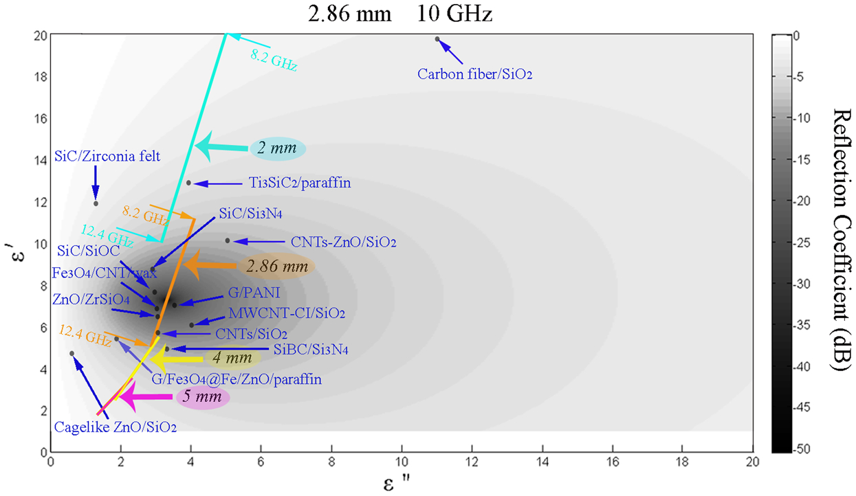
Permittivity of ceramic and other types of materials at 10 GHz: SiBC/Si3N4, 49 Ti3SiC2, 52 Carbon fibre/SiO2, 157 SiC/zirconia felt, 159 Fe3O4/carbon nanotubes (CNT)/wax, 164 MWCNT–CI/SiO2, 165 cagelike ZnO/SiO2, 166 SiC/Si3N4, 183 SiC/SiOC, 185 ZnO/ZrSiO4, 186 G/PANI, 189 G/Fe3O4@Fe/ZnO/paraffin, 190 CNTs/SiO2, 194 and CNT–ZnO/SiO2 211
Electromagnetic (EM) absorbing properties of different ceramic composite materials
Process of Si–C–N based ceramics and composites
Powder technology is the traditional method to prepare ceramics, requiring the presence of sintering additives and high fabrication temperature, which significantly constrains technical applications. In recent years, two main approaches have been developed to fabricate Si–C–N based ceramics: polymer-derived ceramics (PDCs) and CVI.
In the case of the PDC route, preceramic polymers can be converted into ceramic fibres, layers, monolithic ceramic and composites through high-temperature pyrolysis. In principle, preceramic polymers can be processed or shaped by using conventional polymer-forming techniques such as PIP, injection moulding, coating from solvent, extrusion or resin transfer moulding (RTM). 215
Chemical vapour infiltration is a variant of CVD. Chemical vapour deposition is a chemical process used to produce high-purity, high-performance solid materials. In a typical CVD process, a wafer (substrate) is exposed to one or more volatile precursors, which react and/or decompose on the substrate to produce desired deposit. Chemical vapour deposition implies deposition onto a surface, whereas CVI implies deposition within a body. Chemical vapour infiltration was originated in efforts to densify porous graphite bodies by infiltration with carbon. 216 The earliest report of CVI for ceramics was a patent in 1964 for infiltrating fibrous alumina with chromium carbides. 217 The most widely used commercial process is isothermal/isobaric CVI (ICVI) which depends only on diffusion for species transport. They are generally operated at reduced pressure (1–10 kPa) for deposition and transport rate control. 218–220
Various Si–C–N based ceramics were fabricated by PDCs 221–227 and CVI/CVD routes. 228–235 Polymer-derived ceramics 236–243 and CVI/CVD 244–253 have various advantages: (i) the process can be conducted at low pressure and low temperature; (ii) the phase composition of the matrix can be easily designed by the adjustment of the type, concentration and processing parameters of the precursors; (iii) near-net shape components can be fabricated. Therefore, CVI and PDC methods not only have the potential to form A/B/C type ceramics in situ, but also make it possible to fabricate ceramic-based hybrid structure. Figure 33 exhibits the cartoons of the nanodomain structural models for PDCs. 223 Recently, a novel class of filler-loaded cellulose fibre preform, so-called preceramic paper, which can be used for the present applications, was developed. 242 Preceramic paper may serve as a preform to manufacture lightweight as well as multilayer (including functionally graded) ceramic-based composites. Oxide as well as non-oxide ceramics may be processed into single-sheet, corrugated and multilayer structures. In contrast to common paper, preceramic paper contains a substantially higher level of the filler phase up to 90 wt-%%. Applying well-established paper processing technologies, including computer aided manufacturing (e.g., laminated object manufacturing), ceramic structures of complex shape and size can easily be processed, offering a high potential for economical manufacturing. Owing to the versability of chemical compositions, the preceramic paper offers an attractive approach to process ceramics with tailored macro- and microscopic porosities. Dense ceramic composite materials can be obtained, for example, by non-reactive and reactive melt or CVI post-processing. Figure 34 shows the paper-derived ceramic structures. 242 Figure 35 presents a lattice truss sandwich panel structure, which is composed of carbon fibre reinforced SiC matrix composites (C/SiC) fabricated by CVI.
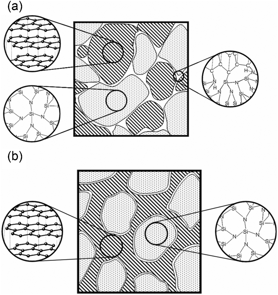
Cartoons of the nanodomain structural models for: a GM35 and b HN1 PDCs. The nanometre-scale amorphous/turbostratic carbon and Si3N4 domains are shown with stripes and dots, respectively, with the interfacial areas as the white regions. b shows a continuous matrix of amorphous/turbostratic carbon with Si3N4 clusters embedded in it. The atomic structures within these domains are shown schematically in the insets. 223 Copyright 2012 US, the USA Chemical Society
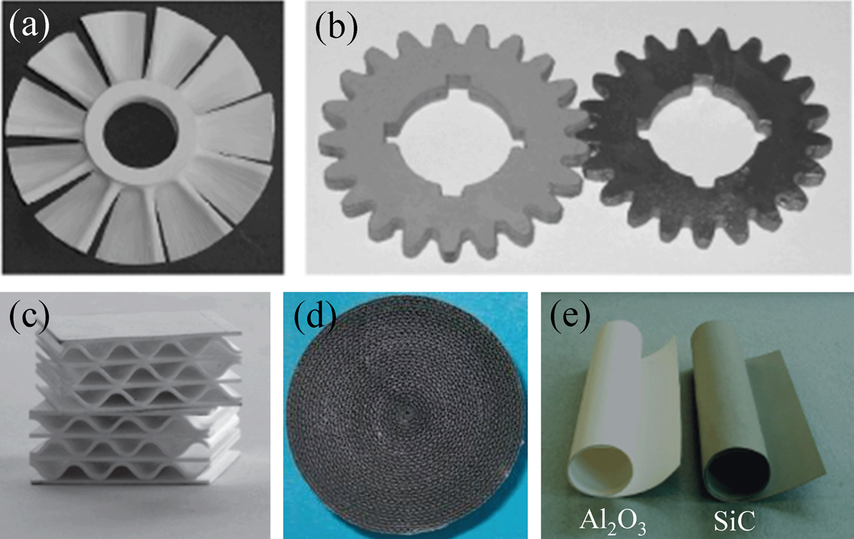
a turbine rotor (diameter: 60 mm) prepared from an Al2O3-filler preceramic paper; b gear wheel (diameter 50 mm) manufactured from SiC-filled preceramic paper; c paper-derived corrugated ceramic structures of laminated Al2O3 heat exchanger; d rolled SiC catalyst carrier; and e the preceramic paper. 242 Copyright 2008 John Wiley and Sons
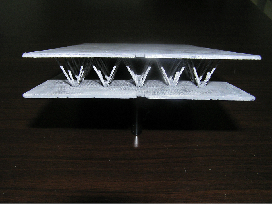
Photo of a C/SiC composite sandwich panel with lattice truss
Chemical vapour infiltration of Si–C–N based ceramics offers a wide range of microstructure to be tailored for optimisation of EM wave properties. Co-deposition of SiC–Si3N4 ceramics by CVI/CVD is an example. At CVI temperature<1000°C, the condensed phase products from SiCl4–NH3–CH4–H2–Ar gaseous mixture include: SiC, SiC+C, Si3N4+C, Si3N4+SiC and Si3N4+SiC+C. With increasing temperature, the condense products were changed from high nitrogen-bearing species to high carbon-bearing species, 235 Fig. 36. It is supposed that catalytic nanoparticles could capture the carbon atoms in the SiC–Si3N4–C co-existing zone in the CVI Si–C–N phase diagram, which may lead to the simultaneous formation of CNTs and SiCN ceramics by CVI. As shown in Fig. 37, simultaneous formation of CNTs and Si–C–N was achieved by CVI using SiCl4–NH3–CH4–H2–Ar as precursor and iron nanoparticles as catalyst, which may provide improved mechanical and EM absorbing properties.
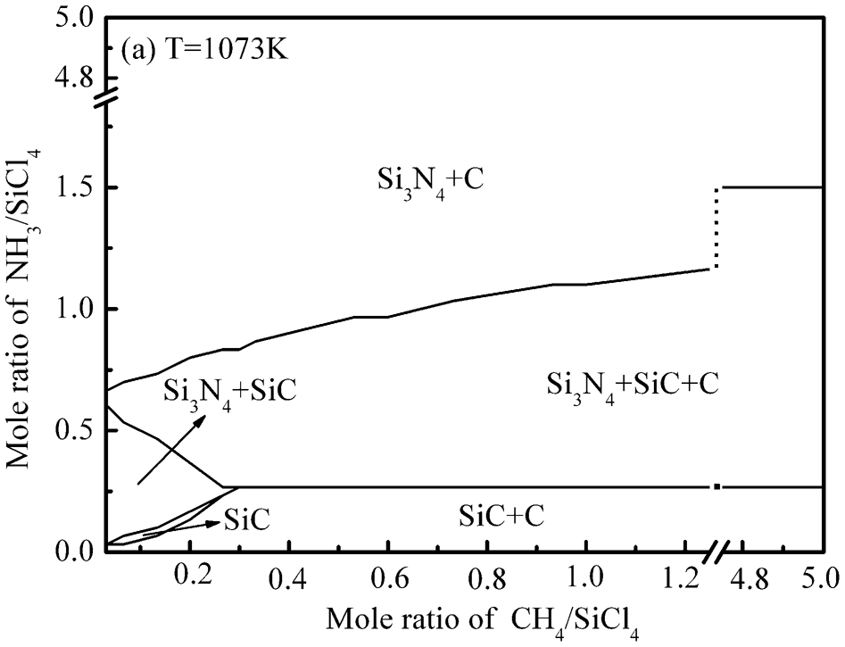
Thermodynamic diagrams of chemical vapour deposition (CVD) SiCN ceramics for SiCl4–NH3–CH4–H2–Ar system at 1073 K, P = 0·01 atm and H2/SiCl4 = 0. 235 Copyright 2012 John Wiley and Sons
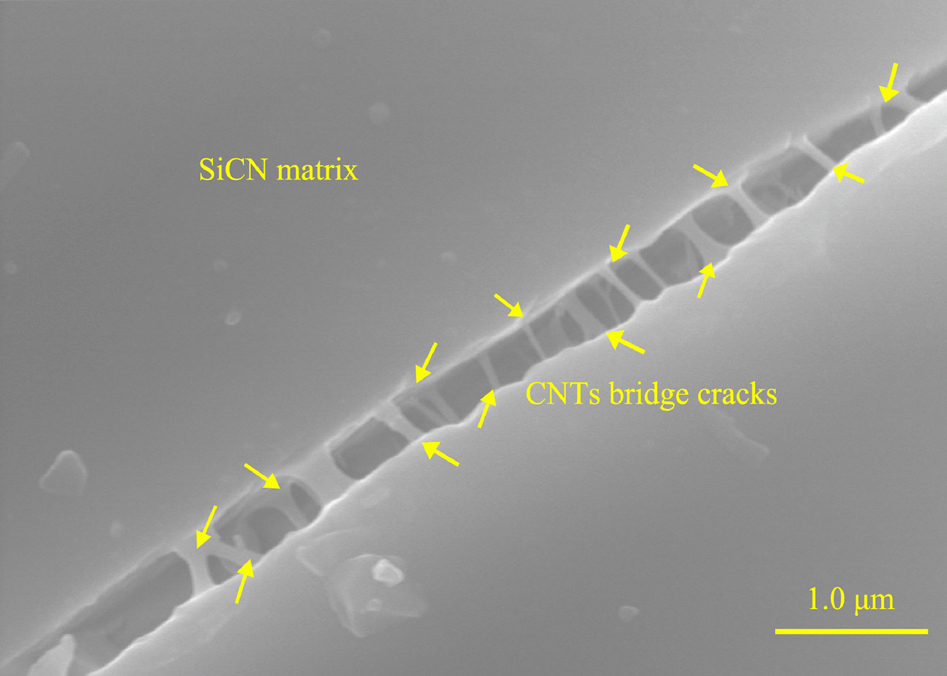
Scanning electronic micrograph (SEM) images of crack bridging by in situ formed carbon nanotubes (CNTs) in SiCN matrix
Applications
Applications of EM transparent ceramics and composites
Electromagnetic transparent ceramics and composites are used as microelectronic packaging materials, radome, antenna window materials and microwave transparent reaction chamber to reduce signal attenuation.
With the widespread applications of microwave heating, microwave metallurgy is becoming a new type of green metallurgical method, possessing many features such as very rapid heating rates, considerably reduced processing times and energy saving. 254 Electromagnetic transparent ceramics and composites are used as supporting units of the heating reactions to ensure an efficient and save metallurgy process.
For converting carbon-based feedstocks such as biomass into liquid fuel, EM transparent ceramics are needed. The system includes at least one reaction chamber, comprising at least one microwave transparent chamber wall and a reaction cavity configured to hold the carbon-containing feedstock. 255 A microwave source emits microwaves that are directed through the microwave transparent wall of the reaction chamber to impinge on the feedstock within the reaction chamber. The reaction chamber can also act in a reactive mode that will convert gaseous carbon feedstock into different gaseous chemical species.
Applications of EM shielding ceramics and composites
Metals and metal oxides traditionally used as EMI shielding materials have higher weight and they provide EMI shielding by reflection of the EM waves, which prohibits them from being used for EMI problems. Lightweight ceramic materials with EMI shielding dominated by absorption provide a better solution to EMI problems.
Electromagnetic shielding ceramics can be used as cases, housings, electronic packaging of highly integrated circuits and wireless communication system. Other harsh environment or high-temperature applications also benefit from a ceramic system. Potential applications include EMI problems resulting from both intersystem and intrasystem.
Intersystem problem includes: radar interference with aircraft navigation systems, power line interference with telecommunication systems, mobile radios interference with television receivers, power line transient interference to computer systems, aircraft radio interference with shipboard systems and long-distance FM and TV transmitter interference with nearby FM and TV transmitters. 256
Intrasystem problems include: interference from an automotive ignition system to a radio receiver within the car, leakage of radar transmitter energy into the radar receiver, interference caused by magnetic field of the tape drive to low level digital circuits within the computer system and interference caused by digital circuits operating from a common power supply with a low level analogue circuit.
By using EM shielding materials, it is possible to cover electronic, medical devices or other devices to isolate them from external and internal EMIs.
Applications of EM absorbing ceramics and composites
Electromagnetic absorbing ceramics and composites are useful as microwave absorbing components in microwave heating, vacuum electronic amplifiers, elementary particle accelerators, passive microwave devices, anechoic chambers, antenna systems, stealth aircraft and ship, for heating, suppressing spurious oscillations, bandwidth control, testing electronic devices and stealth.
In high-power vacuum-electronic-based amplifiers, such as travelling wave tubes and high-peak power X-band gyroklystrons, lossy ceramic materials are used to prevent spurious oscillations, broaden device bandwidth, improve power uniformity across the operating band and facilitate impedance matching. 257–259
In elementary particle accelerators for physics research or medical/industrial purposes, EM absorbing ceramics and composites are used to control higher-frequency modes in the accelerating structures, which would degrade the bunching of the particle beam. 260
In passive microwave devices, they are used as power-absorbing loads and for the damping of higher-order modes in waveguide and stripline-based components. In antenna systems, EM absorbing ceramics and composites are used to damp surface waves, assist in the suppression of spurious radiation lobes and reduce cross-talk between adjacent radiating elements.
Summary and outlook
Si–C–N based ceramics, especially those based on Si3N4 and SiC, containing insulating or conductive secondary phases, are attractive not only for EM transparent but also for EMI shielding and EM absorption applications. These ceramics and composites have great potential to be tailored into materials with ϵ′ lower than 5 and tanδ lower than 0·01 for EM transmission, ϵ′ of 5–20 and ϵ″ of 1–10 for EM absorption, and ϵ′ higher than 20 and ϵ″ higher than 10 for EM shielding.
In order to meet the requirements of EM transmission, tailoring the size and distribution of pores and insulating secondary phase in an EM transparent ceramics is a key factor. By lowering the grain size of secondary phase from micrometre size to nano size, the composites may attain superior mechanical properties, but the dielectric loss increases and hence EM transparency decreases. SiO2, Si3N4, Si3N4–SiO2, Si3N4–BN and Si3N4–SiO2–BN are promising EM transparent materials, which can find applications in microelectronic packaging, radome, antenna window and microwave transparent reaction chamber.
For EM shielding applications, Si–C–N based ceramics have great potential to lower the surface reflection but still keep a high SE owing to the semiconductor characteristics. Actually, most Si–C–N based ceramics may be tuned into EM absorption ceramics, which can be used as shielding ceramics as well. C, SiC, SiC–C, Si3N4–C and Si3N4–SiC are potential EM shielding materials, which can be used as electronic packaging of highly integrated circuits, and be used in wireless communication system, telecommunication base stations and the other electronic devices.
Electromagnetic absorption ceramics are composed of insulating phase and conductive or semi-conductive secondary phase. Different from EM transparent ceramics, nano-size microstructures are preferred in absorbing ceramics. Si3N4–SiBC, Si3N4–SiCN and Si3N4–SiBCN are promising EM absorbing materials, which can be designed into various absorbers for civil and defense applications.
The concept of hybrid structure and EM MMs opens up new avenues for EM absorption. Telecommunication systems use advanced signal processing techniques based on multiple band operation/access. By using hybrid structure and MM structure, both classical broadband absorption and frequency-selective EMI shielding solutions are possible. Si–C–N ceramics containing CNTs may attain electrically adjustable properties, which will increase tunability of the MMs.
Processing of multiphase composite microstructure and hybrid structure with tailored mechanical, dielectric and physical properties mainly refer to CVI/CVD and PDC techniques. Si–C–N based materials and structure with EM properties ranging from transmission to shielding offer a high potential for lightweight, wide bandwidth and multifunctional EM devices.
Footnotes
Acknowledgment
This work is supported by the Natural Science Foundation of China (Grant: 51332004 and 51221001), the Program for New Century Excellent Talents in University (NCET-08-0461), and the 111 Project (B08040).