
Abstract
Hydrogen is expected to become a commonly used energy carrier on the global scale in the near future. However, hydrogen as a fuel is environmentally friendly only when generated from water using renewable energy, such as solar energy. Therefore, intensive research aims to develop a new generation of solar materials, which may be used for the production of hydrogen fuel from water using solar energy. The highly promising candidates for solar energy conversion are photosensitive oxide semiconductors (POSs), particularly the TiO2-based semiconductors, which may be used for converting solar energy into the chemical energy required for hydrogen generation from water, as well as water purification (removal of microbial agents and toxic contaminants from water). The present work considers an R&D strategy for developing TiO2-based systems capable of converting solar energy into the chemical energy via water oxidation. The effect of surface versus bulk semiconducting properties on the performance of POSs is considered in terms of partial and total water oxidation. The progress requires modification of the key performance-related properties (KPPs) in order to enhance the light-induced reactivity of the POSs with water. The most recent approach in the development of POSs with enhanced performance is deposition of metallic islets of different size and shape in order to induce a plasmonic effect. The development of high-performance POSs can be achieved through a multidisciplinary approach. It is shown that defect disorder has a critical effect on the light-induced reactivity of POSs and the solar energy conversion. Therefore, defect engineering may be applied in the development of high-performance POSs. This work considers the hurdles in the development of high-performance POSs for specific applications and formulates the key questions that must be addressed to overcome these hurdles. The concepts developed for TiO2 may be expanded for other metal oxides.
Abbreviations
Auger electron spectrometry
Electrical conductivity
Energy conversion efficiency
Electromotive force
Elastic coil detection analysis
Flat band potential
International partnership for hydrogen economy
Key performance-related property
Low energy electron diffraction
Low energy ion scattering spectroscopy
Localised surface plasmon resonance
Nuclear reaction analysis
Positron annihilation lifetime spectroscopy
Photoelectrochemical cell
Particle-induced X-ray emission
Photosensitive oxide semiconductor
Propagating surface plasmon
Photovoltaic
Rutherford backscattering
Sustainable energy systems
Secondary ion mass spectrometry
Surface plasmon
Surface photovoltage
Thermoelectric power
Work function
X-ray photoelectron spectroscopy
X-ray diffraction
Introduction
According to the US National Oceanic and Atmospheric Administration Station at Mauna Loa, Hawaii, the concentration of CO2 in the atmosphere exceeded 400 ppm for the first time on 9 May 2013. The increase in CO2 levels in the atmosphere during the last three centuries is shown in Fig. 1. 1–3 This data sends a warning signal about the dramatic increase in the atmospheric levels of greenhouse gases that are associated with the combustion of fossil fuels. The resulting climate change is already apparent.

The increase in CO2 concentration recorded by ice probing and direct analysis of the atmosphere. 1–3 The filled point represents the US National Oceanic and Atmospheric Administration reading on 9 May 2013 [www.noaa.gov]
As evident from Fig. 1, the total CO2 concentration increase over the 100 years of the nineteenth century was 15 ppm. In the twenty-first century, it has taken only 5 years of CO2 emission to increase by the same amount. The resulting global warming is associated with Antarctic ice melting, which in turn will result in an increase in global sea levels. In general, global warming results in deterioration of the environment. There is also increasing awareness that the unprecedented increasing rate of fossil fuel use is unsustainable and that world reserves of fossil fuels are rapidly depleted. Consequently, there is an urgent need to develop a non-polluting, and sustainable, replacement for fossil fuels.
Hydrogen is considered to be the fuel for the future. 4,5 The first policy initiative to develop hydrogen technologies was launched by President George W. Bush in his State of the Union Address on 28 January 2003. This initiative led to establishment of the International Partnership for the Hydrogen Economy (IPHE), which aims to produce hydrogen using solar energy and to develop the associated hydrogen technologies (storage, transport, distribution, and security) as well as establish related standards.
The main advantage of hydrogen as a fuel is that it can be generated from water, which is a renewable raw material, since the combustion of hydrogen results in the re-formation of water. However, currently almost all hydrogen produced industrially is by steam reforming of natural gas; the conversion of hydrocarbons into CO and H2 via the endothermic reaction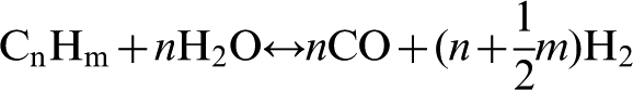
The resulting carbon monoxide then reacts with water vapour and forms hydrogen according to the exothermic reaction
A byproduct of steam reforming of hydrocarbons is CO2.
An alternative approach to generate hydrogen is water electrolysis. However, when the electricity used for electrolysis is produced from the combustion of fossil fuels, carbon dioxide emissions remain problematic. Solutions to this conundrum exist, for example in Iceland, the electricity used to generate hydrogen by water electrolysis is obtained from geothermal power stations. 6
Despite the potential benefits of using hydrogen as a fuel, there are growing concerns about the global impact if steam reforming remains the major source of hydrogen production. Therefore, there is an urgent need to produce hydrogen using renewable energy sources.
The most abundantly available renewable energy source is solar energy. Consequently, intensive efforts to develop technologies for converting solar energy into alternative forms of energy are occurring.
Another consequence of the rapidly deterioration of the global environment is the lack of clean drinking water in many parts of the world. According to UN statistics, over 1bn people have no access to clean drinking water. Consequently, approximately 2·4m people, mainly children, die from waterborne diseases annually. Therefore, there is an urgent need to develop cost-effective water purification technologies that can remove toxic agents, such as bacteria and organic contaminants, from water.
The authors of the present work are members of an international consortium representing the multidisciplinary skills needed in R&D on novel photosensitive oxide semiconductors (POSs) for water oxidation and other environmentally friendly applications. They are involved in a R&D initiative on the generation of solar hydrogen fuel and water purification using solar energy.
The present work considers a research strategy aimed at developing a new generation of materials capable of converting solar energy into chemical energy via water oxidation. The strategy includes both total water oxidation to produce hydrogen in an environmentally clean and sustainable manner and the partial oxidation of water to form active radicals, which have the capacity to remove toxic organic compounds from water.
Postulation of the problem
There has been an accumulation of reports on the development of POSs, which are expected to form a next generation of solar materials. The main advantage of POSs, over the valence semiconductors currently available on the market, is their chemical stability in water. Moreover, POSs are inexpensive, and their performance-related properties can be easily modified by defect engineering. 7–9 The main disadvantage of POSs is, however, a low efficiency for the conversion of solar energy. Therefore, intensive research aimed at developing high-performance POSs is required.
The lack of progress in the development of POSs with the high performance required for commercial application can be considered in terms of the following hurdles:
Lack of theory that may be used to predict the effects of basic properties on performance. Such theory is best developed and validated using well defined experimental data, which are compatible and reproducible. There is a need to collect the necessary well defined data.
Research on POSs overlaps several scientific disciplines, such as solid-state chemistry, surface science and electrochemistry that are traditionally remote in terms of research concepts. Therefore, in-depth understanding of the related properties and phenomena requires multidisciplinary expertise.
The ultimate goal of research on POSs is the development of high-performance photoelectrodes for the generation of hydrogen by water splitting and photocatalysts for water purification using solar energy as the only driving force of the process. This goal may be best achieved through a multidisciplinary approach requiring a critical mass of infrastructure and expertise. The aim of the fundamental research is to generate well defined experimental data, which can be used to develop and validate appropriate theoretical models capable of predicting the effect of bulk and surface properties on performance.
Light-induced water oxidation reactions take place at the surface. Thus, characterisation of the surface using surface sensitive techniques, such as X-ray photoelectron spectroscopy (XPS), secondary ion mass spectrometry, SIMS, Rutherford backscattering (RBS) spectroscopy and low energy ion scattering spectroscopy (LEIS) is crucial. However, the surface is not autonomous. It remains in close contact with the bulk phase and, therefore, there is a close relationship between the bulk and surface properties.
There is growing awareness that nuclear techniques have the capacity to characterise the outermost surface layer. Related nuclear techniques may also be used to modify local surface properties, such as chemical composition, structure and defect disorder. However, since the operation and maintenance of such facilities requires specific expertise, the availability of these techniques is restricted to nuclear research organisations. The application of nuclear techniques in the formation of POSs with the key performance-related properties (KPPs) is considered in Application of Nuclear Techniques in Processing and Characterisation section (below).
The present work provides a brief overview of the reported data on POSs and research strategies in the development of POSs. The focus is on TiO2-based oxide semiconductors. The present work also considers oxide materials that exhibit a smaller optical band gap, such as α-Fe2O3 (haematite) and BiVO4. An attempt is made to identify the barriers to making progress and formulate the questions to be addressed. Finally, this work considers the R&D strategy required for the development of POSs for photoelectrochemical production of solar hydrogen fuel and photocatalytic water purification. The overview is summarised by a list of unresolved problems in the development of POSs for total and partial water oxidation.
Water oxidation
Reaction routes
Water oxidation may be considered in terms of the two reaction routes, which are represented schematically in Fig. 2:
Partial water oxidation route which is associated with the removal of two electrons from two water molecules. This reaction results in the formation of hydroxyl radicals and protons. Charge compensation requires that the two electrons absorbed on the anodic sites are removed at the cathodic sites either through reduction of oxygen or through the formation of hydrogen peroxide.
Total water oxidation route which is associated with the coordinated transfer of four electrons from two water molecules to the surface of the photocatalyst. This results in the decomposition of water into its elemental components, including oxygen and protons. Maintaining charge neutrality requires that the electrons absorbed at the anodic sites are removed at the cathodic sites through the reduction of protons.
The key question is: what are the specific surface sites responsible for either total or partial oxidation of water? So far, very little is known on the specific surface properties required for selective reactions towards either total or partial water oxidation.
The photocatalytic performance of oxide semiconductors for the conversion of solar energy into the chemical energy required for water oxidation is predominantly influenced by the light-induced reactivity of the POSs with water. Therefore, the research strategy for the development of photocatalysts and photoelectrocatalysts with maximum performance is aimed at the modification of their reactivity with water.
It has been documented that the performance of oxide semiconductors in water oxidation may be considered in terms of several KPPs, which are profoundly related to point defects and are interrelated between themselves. 7–9
Total water oxidation
Basic reactions
The formation of hydrogen from water, using solar energy, can occur along several alternative pathways, including:
Photovoltaic pathway.
Photoelectrochemical pathway.
Thermochemical pathway.
Biochemical pathway.
Alternative pathways.
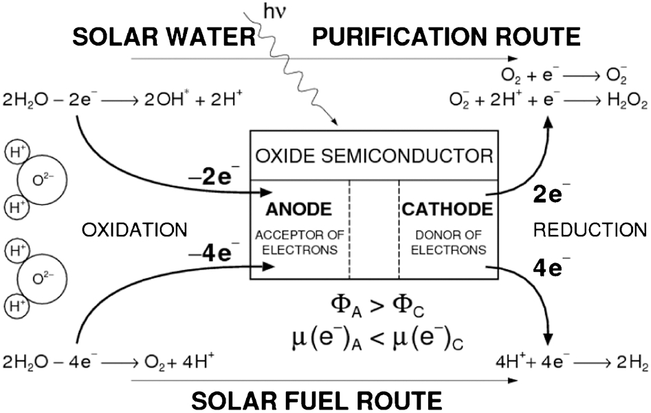
Representation of two water oxidation routes (Φ is the work function (WF), μ(e−) is the chemical potential of electrons, and subscripts A and C are related to the anode and cathode, respectively). Reproduced with permission from Ref. 10. Copyright T. Bak, 2010
So far, the most environmentally friendly method of generating solar hydrogen is by water electrolysis using photovoltaic (PV) electricity. This technology, however, is inconvenient as it requires application of two devices: a PV solar panel producing electricity and an electrolyser. Conversely, a photoelectrochemical cell (PEC) for water splitting requires only one device.
The conceptual design of a PEC is represented schematically in Fig. 3. Although their efficiency is currently below the level required for commercialisation, a substantial increase in the energy conversion efficiency (ECE) has been recently achieved. 11 The ECE of the system reported by Kashelev and Turner 12 was larger (12%); however, the performance of their device rapidly deteriorates because of corrosion. A key aim of the research is the development of a PEC with enhanced ECE and high chemical stability. A critical element of the PEC is the photoelectrode, which is made of a POS.
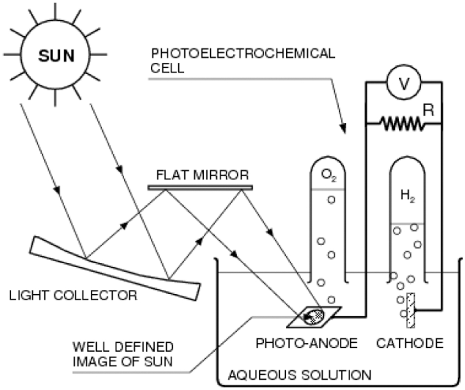
General concept of photoelectrochemical water splitting using sunlight. Reproduced with permission from Ref. 10. Copyright T. Bak, 2010
Fujishima and Honda 13 were the first to show that water may be split using TiO2 as a photoanode. Since then, TiO2 has been considered as one of the most promising candidates for water photolysis, although its high band gap (3 eV) has guided the search for alternatives that can absorb light of lower energy but higher intensity in the solar spectrum.
The process of solar water splitting requires multi-electron transfer between the anodic site of a semiconducting oxide surface and adsorbed water molecules.
14
Under neutral and acidic conditions water oxidation can be described by the following reaction
Under alkaline condition oxygen evolution takes place according to the following reaction
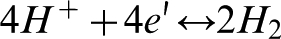
In the case of neutral or alkaline solution hydrogen evolution may be represented by the following reaction
Reactions (3) and (4), which are associated with the transfer of four electrons per two water molecules, represent total water oxidation.
Numerous studies have aimed to develop systems with enhanced ECE. According to the US Department of Energy, an ECE of 10% may be economical. 15 While higher efficiencies have been reported, these are either too expensive or unstable in aqueous environments.
The key requirement for total water oxidation is the coordinated removal of four electrons from two water molecules. This is not easy since water is a very stable compound. The transfer requires optimisation of both the collective factor, such as the Fermi level and the local factor, which can be considered in terms of atomic site lattice elements. In the case of TiO2, titanium vacancies are considered to be surface active sites. 16 The mechanism of total water oxidation in the presence of such active sites is represented schematically in Fig. 4.
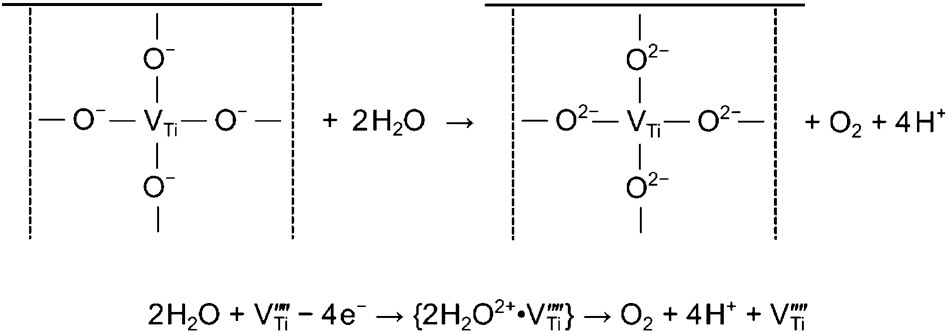
Schematic representation of total water oxidation and the associated multi-electron charge transfer at titanium vacancy acting as an active site
Photoelectrochemical water splitting is very attractive for the following reasons:
The raw material for the production of solar hydrogen is water, which is renewable.
Solar hydrogen is generated using solar energy, which is a nearly infinite energy source.
Both the generation and combustion of solar hydrogen are environmentally friendly. Combustion of hydrogen results in the re-formation of water.
The reports, which have accumulated so far, allow the following points to be made:
Promising candidates for the conversion of solar energy into chemical energy are oxide semiconductors. Research has mainly concentrated on TiO2-based systems as well as other transition metal oxides such as α-Fe2O3 and ternary oxides. The advantage of these systems is their low cost and high resistance to corrosion and photocorrosion in water. Only in the absence of corrosion can the photocatalyst exhibit a stable performance over a long period.
There has been an accumulation of conflicting reports on the properties and performance of metal oxides. It is shown below that this is mainly because of lack of well defined and reproducible data. There is a need to collect data for well characterised samples that can be used to develop theoretical models. Such models can be applied for predicting the effect of the properties, including the KPPs, on performance.
Cost-related aspects
The commercialisation of the solar hydrogen technology is critically determined by cost-related matters. At present, hydrogen is mainly generated by the conversion of natural gas. The direct costs of hydrogen generation using this method are relatively low. Awareness is growing, however, that the indirect costs, associated with the generation of hydrogen from natural gas, are high. These include the costs related to the damaged environment, such as extreme weather conditions and the associated costs in the production of food, increased pollution of air, water and soil and the impact of pollution on health and productivity. So far, these costs, which are substantial, are borne by the community. Governments are beginning to protect the community from pollution-induced health problems, for example, the government of California undertook legal action against car manufacturers (powered by gasoline) in 2009. 17 This action was reflective of the community pressure applied on governments to reduce pollution by vehicles powered by fossil fuels. There is an increasingly urgent need to develop solar hydrogen fuel, which is environmentally clean in both its generation and combustion.
The production cost of hydrogen by steam reforming of methane is approximately $6/GJ. 17 On the other hand, the cost of solar hydrogen production using PV electricity is $28/GJ. 17 This figure is higher than the cost of hydrogen production from natural gas by the factor of 4·7. However, taking into account that the costs associated with air pollution resulting from combustion of fossil fuels is equivalent to $33 GJ, the solar hydrogen fuel is the ultimate winner.
At present, solar hydrogen is generated mainly by water electrolysis using PV electricity. This approach, however, is inconvenient as it requires two devices: electrolyser and PV cell. The development of a device, which allows water photolysis using a single device, PEC is important. So far, however, the ECE of the PECs based on oxide semiconductors remains below the level required for commercialisation.
Partial water oxidation
Partial oxidation of water may be achieved when only two electrons are removed from two water molecules. A schematic representation of partial water oxidation and the related charge transfer is shown in Fig. 5.
The theoretical model of partial water oxidation on the TiO2 surface. Reproduced with permission from Ref. 10. Copyright T. Bak, 2010
The primary products of partial water oxidation are hydroxyl radicals and protons
Alternatively, water oxidation reaction results in the formation of hydrogen peroxide
The charge neutrality requires that the two electrons generated at the anodic sites are removed at cathodic sites. This is possible, e.g., through the reduction of oxygen (dissolved in water)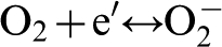
An alternate reaction occurring at the cathodic site is reduction of the superoxide species leading to the formation of hydrogen peroxide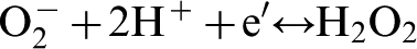
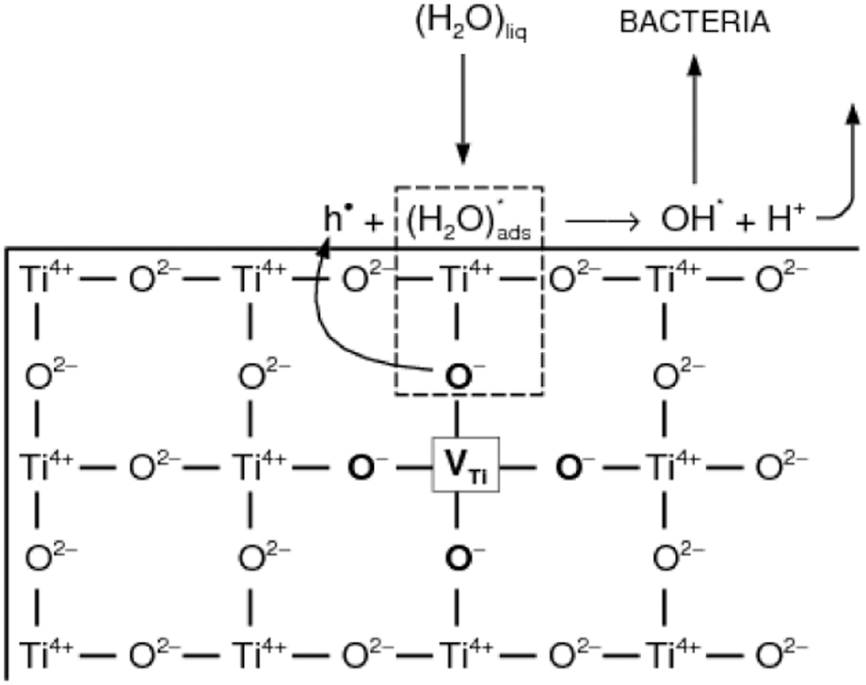
The species formed as a result of processes (5)–(8) are described as reactive photo-induced species. These species exhibit high reactivity with organic compounds, including microbial cells and other toxic organic contaminants. The hydroxyl radical species exhibits the highest oxidation power, which leads to irreversible damage of microbial cells, even when the radical is present at low concentrations. However, because of their high reactivity, the hydroxyl radical species tend to react between themselves before they can diffuse more than one nanometre away from the site of their formation at the TiO2/H2O interface
The superoxide species are less reactive and their diffusion distance is up to one micrometre. These species may penetrate the microbial cell walls through porins. 18 The hydrogen peroxide species, which are substantially less reactive, may be transported over a distance of approximately 1 mm. These species may also penetrate the cell wall. Inside the microbial cell, these radical species are involved in intra-cell chemistry leading to the death of the cell chain.
In the presence of ferrous iron, which is released from iron-sulphur cluster proteins, both superoxide and hydrogen peroxide species react leading to the formation of hydroxyl radicals (Haber–Weiss reaction)
The mechanism of the intra-cell reactivity, involving iron, may be represented by the Fenton-type reaction
The superoxide species are then used to reduce the Fe3+ species into Fe2+ species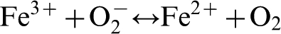
Even if the oxidation power of both superoxide and hydrogen peroxide species, which are formed at the TiO2/H2O interface, is relatively low, their ability to penetrate the cell wall leads to the formation of the hydroxyl radicals within cells. The details on the structures, properties and reactivity of microbial agents as well as the biocidal activity of TiO2 have been reported elsewhere. 18
The strategy in the development of high-performance photocatalysts for water purification (disinfection and detoxification) consists of forming oxide semiconductors, which exhibit selective oxidation of water resulting in the formation of a high concentration of active radicals. This can be achieved when the rate of the primary reaction (5) is high.
Spin-off applications
The photocatalytic effect of TiO2 presents the possibility of environmentally friendly coatings, such as antiseptic coating, self-cleaning coatings and anti-pollution coatings. 19 Antiseptic coating can be utilised to kill microbial agents in hospitals and sanitary areas. It is well known that bacteria and viruses are commonly present in hospital walls, where they multiply and propagate out of control. This can be tackled by the use of ceramic or glass tiles coated with a thin layer of TiO2. As a result of the photocatalytic effects, the bacteria and viruses may be removed from the surface in the presence of light and humid air. According to Fujishima et al., 19 the conventional ceramic tiles covered with TiO2 have the capacity not only to kill bacteria on the tile surface very effectively but also to reduce the concentration of bacteria in air.
The self-cleaning coating can be used to break down organic (oily and resinous) films, which trap dirt, on building materials. Finally, TiO2 coatings may also be used to oxidise organic contaminants in air, which is a source of air pollution in urban areas.
Photosensitive oxide semiconductors: example of TiO2
Effect of lattice imperfections on reactivity
The structures and phase compositions of photoelectrochemical and photocatalytic systems are commonly considered to determine their properties. Therefore, the related approach in the development of new systems for solar energy conversion is based on the selection of phases and structures with promising properties.
There is growing awareness that the promising properties of non-stoichiometric compounds can be tuned by the manipulation of structural imperfections within specific crystalline structures. Such a strategy may be used to tailor defect-related properties, such as adsorption, chemisorptions, transport kinetics of mass and charge and the related semiconducting properties, in order to achieve optimal performance. The effect of point defects on the properties of non-stoichiometric oxides at elevated temperatures is described in the fundamental treatise of Kofstad. 20
It is well known that defect-free compounds are not reactive at all or their reactivity is limited. According to Henrich and Cox, 21 perfect surfaces of TiO2 are less reactive with water and oxygen than defected surface. In other words, point defects play a crucial role in adsorption of water and oxygen molecules, their subsequent chemisorption and the related charge transfer. Evidently, knowledge of structural imperfections is essential for understanding the reactivity of oxides, which may be modified in a controlled manner by defect engineering. 7
Defect disorder versus semiconducting properties
Semiconducting properties are closely related to defect disorder. It has been documented that electrical properties, such as thermoelectric power (TP) and electrical conductivity (EC) of oxide materials, are determined by the concentration of point defects. 20 TiO2 is no exception. TiO2 can contain a wide and complex range of ionic defects, including oxygen vacancies, titanium interstitials and titanium vacancies of different ionisation degrees. 9 The list of the predominant defects in TiO2, along with the host lattice elements, is given in Table 1.
Ionic and electronic defects in TiO2 according to the Kröger–Vink 22 and the traditional notation
At elevated temperatures, defects may be assessed using defect equilibria. The equilibria between the predominant intrinsic defects in TiO2, and their associated equilibrium constants, are shown in Table 2.
Basic defect equilibria in TiO2
n and p denote the concentration of electrons and electron holes, respectively, 9 where n denotes the concentration of electrons, p(O2) is oxygen activity and ΔH° and ΔS° denote the free enthalpy and free entropy terms, respectively.
The slopes of log n versus log p(O2) are reflective of the specific defect equilibria assuming that the related defects have the predominant effect on properties.
A combination of equilibria (1)–(5) in Table 2 may be used to derive a defect disorder diagram showing the effect of oxygen activity, p(O2), on the concentration of both ionic and electronic defects. This diagram is shown in Fig. 6.
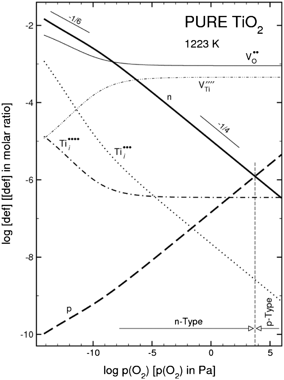
Defect disorder diagram representing the effect of oxygen activity on the concentration of ionic and electronic defects for pure TiO2 at 1223 K 9
Defect disorder may be used to develop TiO2 that exhibits well defined semiconducting properties. 7–9 Figure 6 may be used to determine the effect of oxygen activity on the Fermi level, which is shown in Fig. 7. Alternatively, imposition of variable oxygen activity may be used to process TiO2 with controlled Fermi level that is required for specific applications.
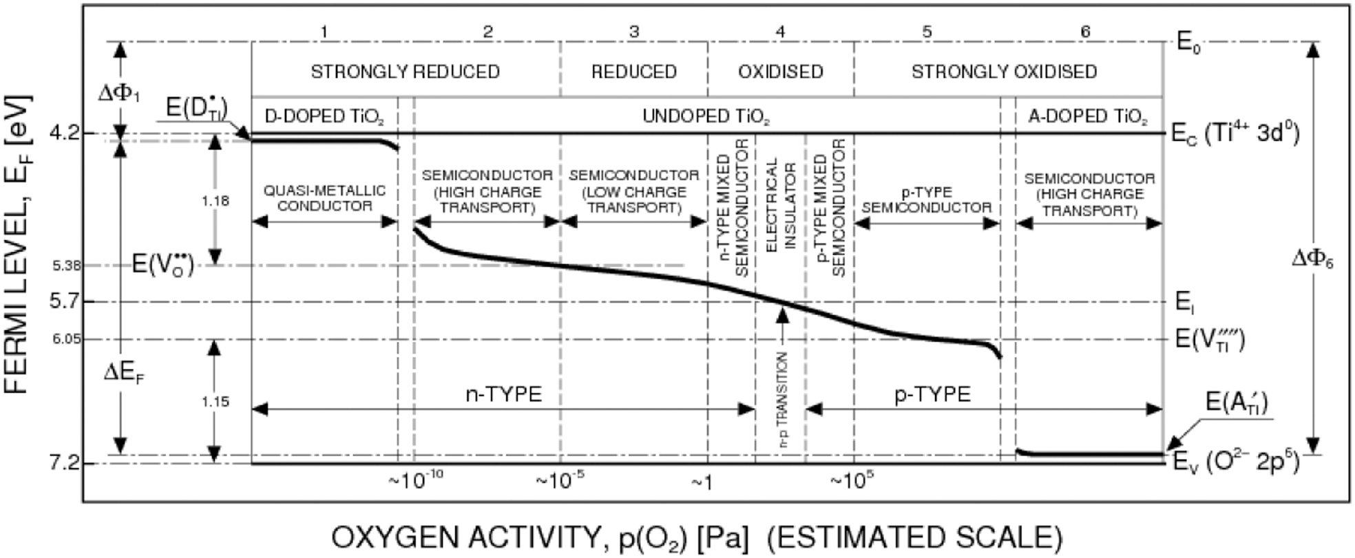
The effect of oxygen activity and doping with donors and acceptors on the Fermi level for TiO2. 9 Reproduced with permission from Ref. 10. Copyright T. Bak, 2010
Modifications of defect disorder and defect-related properties of TiO2
A wide range of approaches to modify the performance of oxide semiconductors for light-induced water oxidation have been reported. These include:
Imposition of variations of the oxygen activity resulting in a shift of the equilibria (1)–(5) in Table 2. These data do not include the effect of hydrogen, which is substantial when the oxide is immersed in water. 23
Incorporation of aliovalent ions, forming donors and acceptors, leading to a decrease and increase of the Fermi level, respectively. The collective factor, such as the Fermi level, of oxide semiconductors may be modified by changes of either oxygen activity or the incorporation of aliovalent foreign ions. As shown in Fig. 7, modification of the oxygen activity alone may lead to changes in the Fermi level by 1·1 eV. The incorporation of donor- and acceptor-type ions may shift the Fermi level to the vicinity of conduction and valence bands, respectively.
Loading the surface with small islets of noble metals. 7,24 Their function is to enhance the cathodic processes involved in the removal of electrons from basic TiO2.
Loading the surface with other small catalyst particles to enhance the cathodic or anodic processes. 7
Collective versus local properties
The primary reaction of water oxidation, which is associated with removal of electrons from water molecule, takes place at anodic sites. The required acceptor-type properties of the anodic site can be achieved by both collective and local properties.
The collective property is determined by the Fermi level related to the outermost surface layer. The lower the Fermi level the stronger the affinity of the surface to electrons. The key quantity that is reflective of the Fermi level at the surface is the work function (WF). There have been efforts to utilise WF measurements to monitor the charge transfer associated with the reactivity of TiO2-based semiconductors with water. 7,9
The local property is determined by a specific surface site at an atomic scale. The properties of the local site are determined by the electrostatic field of individual lattice elements, such as cations and anions, as well as lattice point defects, such as ion vacancies and interstitials. For example, Ikuma et al. 24 investigated the photocatalytic properties of differently oriented single crystal surfaces of TiO2 with respect to the decomposition of linoleic acid. The highest activity was found for the (001) surface.
The reactivity of oxide semiconductors for water oxidation must be considered in terms of both anodic and cathodic reactions. The basic oxidation reactions (3) and (5) take place at the anodic sites. The cathodic reactions (4) and (6) are essential for charge neutrality.
As the result, the reactivity of the surface must be considered in terms of a combination of both local and collective factors. The latter represents the surface properties as a continuum. A typical collective factor is the chemical potential of electrons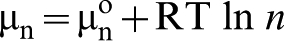

Furthermore, the collective factor, which is determined by the concentration of electrons at the outermost surface layer, exhibits substantial changes (fluctuations) along and across the surface. 27 Therefore, the anodic and cathodic sites must be considered in terms of the surface sites, which exhibit low and high WFs, respectively. The demarcating (critical) WF value is characteristic for specific systems and is determined by charge neutrality. 7
The properties of the local active sites, related to specific ions, are more difficult to identify and characterise. These are dependent on (i) the properties of the specific sites, (ii) the properties of neighbouring ions, and (iii) the crystal field that is reflective of lattice deformations.
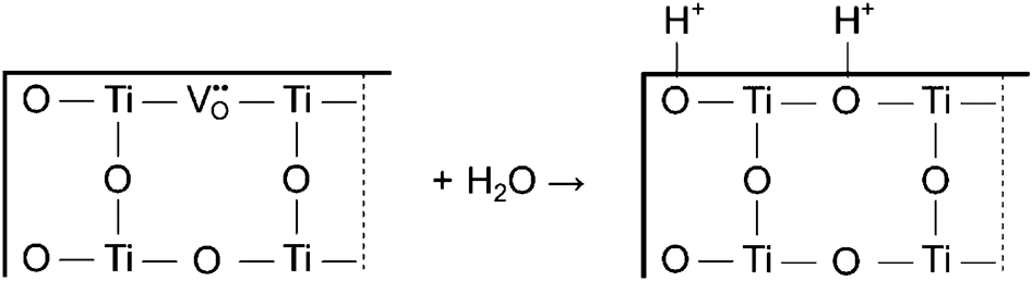
Oxide semiconductors immersed in water interact with water molecules and water decomposition products, involving protons, hydroxide, oxygen and superoxide species. It has been documented that the reactivity of TiO2 with water results in the incorporation of protons into the oxide lattice. 23 The reaction of protons and the n-type TiO2 lattice leads to the formation of a low-dimensional surface structure of H4TiO4. 23 Accordingly, the reactivity of TiO2 with water must be considered in terms of the interactions between water molecules adsorbed on the H4TiO4 surface structure and this structure. It is of interest to investigate if the behaviour observed in TiO2 is seen in other oxides and oxynitrides.
Surface science approach
The surface properties of metals are relatively well defined when the surface is cleaned from adsorbed molecules. On the other hand, studies of metal oxides are more complex since the procedures used for cleaning the surface generally modify the surface properties.
The very initial step of the reactivity of TiO2 with water at room temperature involves water adsorption and subsequent chemisorption associated with charge transfer. The surface of TiO2, if free of defects, is either not reactive at all or its reactivity is limited to physical adsorption. 21,28 Bourasseau et al. 29 reported extensive studies on the light-induced reactivity of TiO2 with oxygen.
Analysis of the reported data allows the following points to be made:
The (110) surface of stoichiometric TiO2 exhibits weak reactivity at room temperature. Under these conditions, its reactivity with water is limited to physical adsorption (upon heating the water molecule may dissociate). 28
Oxygen interacts with the TiO2 surface at room temperature, leading to adsorption, mainly at the active sites formed by oxygen vacancies. Reduction of iO2, leading to an increased concentration of oxygen vacancies, results in dissociative oxygen chemisorption where the charge transfer occurs between the adsorbed oxygen species and the surface Ti3+ ions.
Water molecules dissociate on defective surface of reduced TiO2. 21,28
The reactivity of TiO2 is profoundly influenced by point defects. 7 The reported effects have been associated mainly with oxygen vacancies and titanium interstitials. So far, little is known about the effect of titanium vacancies on reactivity. While there is no agreement between the reported data and the derived reactivity models, there is consensus that perfect or nearly perfect surfaces, which are relatively free of defects, are unreactive at room temperature.
Menetrey et al. 30 proposed that the preferred sites for water adsorption are oxygen vacancies, where the oxygen of the water molecule fills the oxygen vacancy leading to the formation of an OH− group and the remaining hydrogen is adsorbed on the nearby surface oxygen ion as is represented schematically in Fig. 8. While this mechanism explains water adsorption, it does not explain the charge transfer associated with mechanisms (3) and (5). Henrich and Cox 21 suggested that OH− group is adsorbed on a surface titanium ion site, and the remaining hydrogen is adsorbed on a surface oxygen ion.
Theoretical model of water reaction with the TiO2 surface
Experimental data obtained using surface sensitive tools, such as AES, XPS, UPS, SIMS and LEED, indicate that the reactivity of oxide semiconductors, such as TiO2, is determined by structural imperfections, rather than the crystalline structure itself. 7,21
One of the most surface sensitive tool is surface ion mass spectrometry (SIMS) that can be used for the determination of concentration gradients within the outermost surface layers.
Low-dimensional interface structures
There is growing awareness that segregation in crystalline solids results in a substantial enrichment of the surface by specific elements. When the concentration of segregated species at the surface surpasses a certain critical limit, the structure of the surface layer is deformed leading to the formation of a low-dimensional surface structure that can exhibit unique properties different to those of the bulk phase. 31
It has been documented that segregation of indium in indium-doped TiO2, results in the formation of In2TiO5-type surface structures within the outermost surface layer. 32 Studies of surface versus bulk electrical properties, including WF (surface) and TP for Cr-doped NiO indicate that Cr segregation results in the formation of a NiCr2O5-type surface structure. 33 Similar effect has been observed for Cr-doped CoO, 34,35 where a CoCr2O5-type low-dimensional surface structure forms. Comparative studies of TP for polycrystalline and single crystal TiO2 indicate that grain boundaries of polycrystalline TiO2 are enriched with electrons by the factor of 4–13. 36 Tao et al. 37 have shown that the electronic structure of the outermost surface layer of pure TiO2 is different from that of the bulk phase. Understanding of this effect is crucial in better understanding of the light-induced reactivity. These findings indicate that the defect disorder of TiO2 represented in Fig. 6 is reflective of the bulk phase, while the defect disorder for the interface layer is entirely different. The formation of TiO2-based applied systems with enhanced performance requires the determination of defect disorder for the layers in the vicinity of interfaces.
It has been documented that the segregation-induced enrichment of the surface layer in solutes is profoundly influenced by oxygen activity. The thickness of the quasi-isolated surface structure is limited to 1–2 lattice layers. This surface structure is mainly responsible for photocatalytic activity. Therefore, the characterisation of the local properties of this layer and its reactivity with water is crucial for the development of the next generation of TiO2 photocatalysts. 9
Charge transport
The charge transport in oxide semiconductors is associated with the mobility of both electronic and ionic charge carriers. The most common way to determine charge transport is measurement of the electrical conductivity that is the product of the concentration of electronic charge carriers and their mobility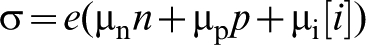
The effect of charge transport on the performance of oxide semiconductors as electrodes and photoelectrodes is substantial because of the following reasons:
The transport of light-induced electronic charge carriers from the site of their generation (by ionisation over the band gap) to the reaction sites at the surface. Specifically, the electrons and electron holes must be transported to cathodic and anodic sites, respectively.
The charge transport-related energy losses must be minimized in order to maximize the performance.
While niobium doping may result in a substantial increase in the concentration of electrons, its effect on the photoreactivity of TiO2 is not clear. First, the effect of niobium on charge transport depends on oxygen activity (in the TiO2 lattice); under reducing conditions, it is substantial as a result of electronic compensation of niobium. However, the effect of niobium on charge transport at high oxygen activity, resulting in ionic charge compensation, is very small, if at all. Second, the effect of niobium ions at the surface is not clear. The surface active sites can be considered as isolated titanium vacancies or defect complexes involving both titanium vacancies and niobium ions in their lattice sites.
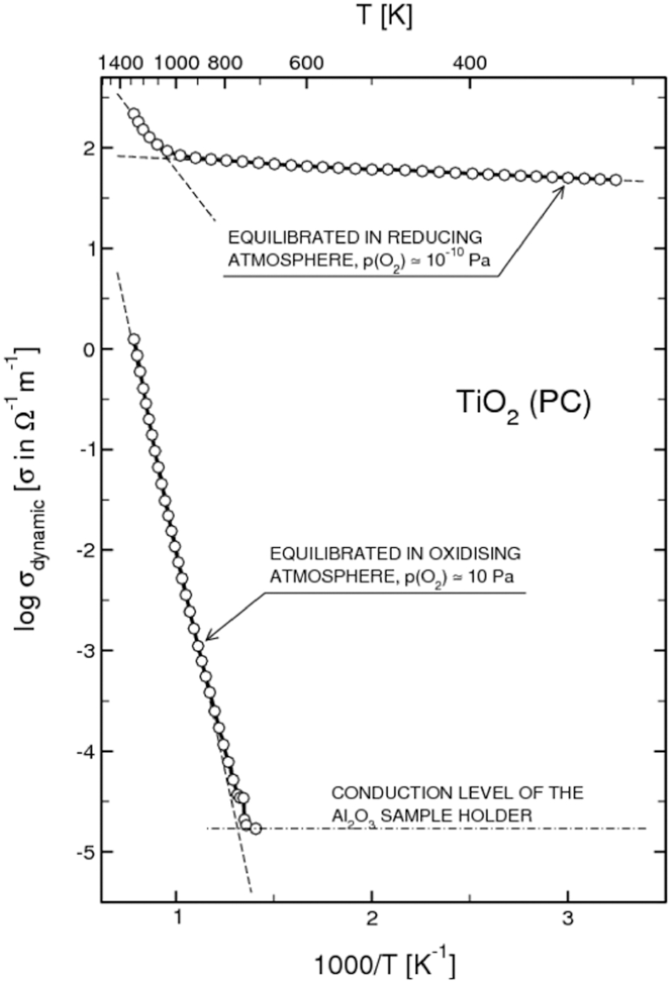
Effect of oxygen activity on the electrical conductivity of pure TiO2 (polycrystalline) at elevated temperatures. Reproduced with permission from Ref. 10. Copyright T. Bak, 2010
Charge transfer
The key function of the anodic site is the transfer of electrons from the adsorbed water molecules to the oxide surface. The ability of TiO2 to charge transfer may be modified by a change in either collective, such as the Fermi level, or local factors, such as the concentration of specific surface elements.
Charge transfer at anodic site
The charge transfer may be increased by lowering the Fermi level of the anodic site. The lower the Fermi level the larger the driving force to transfer electrons from the water molecule to the surface. Efficient charge transfer also requires that the water molecule is adsorbed on a site, which has the capacity to attract electrons, such as a titanium vacancy. 8,9 Charge transfer may be considered in terms of the formation of an active complex, which in the case of total water oxidation, is decomposed into oxygen and protons. Charge transfer may be enhanced by the presence of secondary phases, such as IrO2, which is one of the most commonly described catalyst for the oxygen evolution reaction. Do et al. 38 and Martin et al. 39 postulated that surface loading with small islets of nanoparticulate of metals and metal oxides, acting as a co-catalyst, improves water splitting by suppressing water formation thus allowing the forward reaction, and improving charge separation.
Charge transfer at cathodic site
The key function of the cathodic site is to provide electrons to the adsorbed oxygen molecules (see reaction (7)) or other oxidant. The transfer of electrons from TiO2 to the oxygen molecules requires that the Fermi level of the cathodic site is elevated above a certain critical level. For efficient charge transfer, oxygen molecules should be adsorbed on sites that favour the transfer of electrons from the surface of TiO2 to the oxygen molecules. Such sites are formed by donor-type defects, such as oxygen vacancies and titanium interstitials. Frequently, the electrons at cathodic sites are scavenged by small islets of secondary phases, such as noble metals. 24,38–42
Efficient charge transfer associated with the anodic and cathodic reactions (3)–(6), as well as the charge transport required to remove the electronic charge carriers from the reactive sites, are crucial in the formation of a high-performance photocatalytic system. In some instances, metals, such as Pt, are applied as electrical leads and contacts. It is frequently assumed that these electrodes are not reactive. However, it has been established that platinum reacts with air, leading to the formation of a PtO2 layer, as well as with some oxide semiconductors, leading to the formation of mixed phases. 42 These phases may form a pathway for the charge transfer between TiO2 and the leads.
Plasmonic effect
Small islets of noble metals deposited on the surface of semiconducting catalyst, can act as co-catalysts and enhance the photocatalytic activity. These islets can remove the excess of charge and consequently lead to enhanced charge separation.
Recent studies show that such surface metal nanoparticles (MNP) may enhance the electric field in their vicinity. 43,44 This may boost excitation of electron–hole pairs in semiconducting oxides such as TiO2. The metallic particles may also be involved in a plasmonic effect, which can be considered in terms of light-induced collective oscillations of electrons. These metal particles act as nano-antennas, which can harvest the light energy. This energy is transferred to the valence band and leads to a plasmon-induced ionisation over the band gap. The plasmonic effect is closely related to the shape and size of the surface metal islets. 43 In other words, since different size and shape of metal particles corresponds to different photon energy, the entire solar spectrum may be covered if the surface is covered with metal particles involving a wide range of sizes and shapes.
The surface plasmons (SPs) are coherent oscillations of free electrons at the boundaries between metals and dielectrics, and can be categorised as propagating surface plasmons (PSPs) and localised surface plasmons (LSPs). The localised plasmon resonance frequency of a single metallic nanoparticle can be shifted through alterations in shape, size and surrounding medium. Nevertheless, in nanoparticle ensembles, additional shifts as a result of electromagnetic interactions between the localised modes can be obtained, these interactions are basically of a dipolar nature (when d<<λ). Therefore, the nanoparticle ensemble can be treated as an ensemble of interacting dipoles, which can be embedded into a host matrix as one-, two- or three-dimensional arrays. Electromagnetic coupling of those arrays is possible if the particles are closely spaced and allows for interesting effects such as, enhancement process because of field localisation in nanoparticle junctions.
Metallic nanoparticles with sizes smaller than the wavelength of light show strong dipolar excitations in the form of localised surface plasmon resonances (LSPRs). Localised surface plasmon resonances are non-propagating excitations of the conduction electrons of metallic nanoparticles coupled to the electromagnetic field.
Localised surface plasmon resonance-enhanced visible light hydrogen generation has been demonstrated for metal-TiO2 photocatalysts. The intense localisation of plasmonic near-fields close to the metal-TiO2 interface, coupled with optical transitions involving localised electronic states in TiO2 brings about enhanced optical absorption and the generation of electron–hole pairs for photocatalysis. In summary, the trapping and coupling of LSPR energy efficiently to the TiO2 photocatalyst by proper choice of metals, shape, size and geometry is also one of the promising approaches to achieve high-performance photocatalysis. Thus, it is worthwhile to study the photon and electrically induced chemical reactions at the surface to improve parameters such as reaction rates, charge transport, light absorption, and surface area of photocatalysts and to understand the mechanisms by which they work.
The PSPs can be excited on metallic films, whereas, LSPs can be excited on metallic nanoparticles. The plasmon resonance effect of gold and silver nanoparticles has been studied widely. 45–47 Gold nanoparticles exhibit a plasmon resonance in the visible light range at a wavelength between about 500 and 650 nm depending on their size, whereas, silver nanoparticles show a plasmon resonance at about 400 to 480 nm depending on their size. 46,48 It is well known that the size and shape of the nanoparticles influence the plasmon resonance effect. Gold nanorods are known to have a plasmon resonance at about 750 nm, depending on the aspect ratio of the rods. 47 Silver nanoplatelets can have plasmon resonance at above 500 nm. 47,48 Nanoparticles of other metal, such as platinum, also show a plasmon resonance effect, but they are often in the ultraviolet region, e.g. about 290 nm for platinum nanoparticles. The plasmon resonance effect within the visible light region can, therefore, have significant influence on the performance of photocatalytical cells because of the absorption and/or enhancement of particular wavelengths of the visible light spectrum.
Key performance-related properties
The ECE of photoelectrochemical and photocatalytic oxide systems in solar energy conversion may be considered in terms of the following KPPs: 9
Electronic structure
Surface Fermi level
Population of surface active sites
Near-surface electric field
Charge transport
Charge transfer
Electronic structure (KPP-1)
The electronic structure is the key property that has an effect on light absorption (band gap) and the light-induced reactivity of oxide semiconductors. The latter property depends on the position of energy levels of oxide semiconductor and the electrochemical energy levels of the aqueous electrolyte.
The band gap is the property that controls light absorption leading to the generation of electron–electron–hole pairs by band gap ionisation. The band gap of commercially available rutile, which is approximately 3 eV, allows only a small fraction of the solar spectrum to be absorbed. Reduction of the band gap to approximately 1·8–2 eV is needed to maximise absorption of sun light. This may be achieved by doping with foreign ions, such as niobium, iron, chromium, molybdenum, carbon, boron and sulphur.
Charge transfer within photoelectrochemical systems formed by POSs immersed in aqueous electrolytes depends on the difference between the energy of the bottom of the conduction band (E C) and reduction of the electrochemical couple [E(H+/H2)] as well as the difference between the energy of the top of the valence band (E V) and the oxidation of the electrochemical couple. Spontaneous charge transfer requires that E C>E(H+/H2) and E(O2/H2O)>E V. The charge transfer may be modified by shifting the positions of the E C and the E V through doping of TiO2 with foreign ions.
Surface Fermi level (KPP-2)
The Fermi level may be considered as the chemical potential of the electrons within the POSs. While the electrochemical potential in equilibrium is the same across the surface and the bulk, the chemical potential is not. The Fermi level of the outermost surface layer of POSs, which is different than that of the bulk phase, has a profound effect on the reactivity of POSs and the related charge transfer. The Fermi level of the outermost surface layer may be determined using WF measurements. Work function measurements may also be used for monitoring the Fermi level during chemical reactions and to study the reaction kinetics and the associated charge transfer.
The performance of the anode requires that its surface has a tendency to accept electrons from the water molecule. This may be achieved when its Fermi level is relatively low. Conversely the performance of the cathode requires that its Fermi level is high. Then the surface has a tendency to donate electrons.
The position of the Fermi level may be modified in a controlled manner by variation of oxygen activity in the oxide lattice and the concentration of aliovalent ions incorporated into the lattice. For example, amphoteric semiconductors, such as TiO2, may be modified to form both n- and p-type TiO2 with controlled Fermi level position. The latter case opens an opportunity to form a PEC equipped with two photoelectrodes (photoanode and photocathode) made of n- and p-type TiO2, respectively. Such cell would not require a bias voltage to split water (see below).
The surface Fermi level may be radically modified by imposition of a low-dimensional surface layer. Such surface layer may also be formed as a result of segregation when the segregation-induced enrichment surpasses a certain critical limit corresponding to the surface miscibility limit dictated by the local thermodynamic conditions.
Population of reactive surface sites (KPP-3)
While the Fermi level is considered a collective property, which is related to the surface as a continuum, the reactivity of the surface with water strongly depends on local properties of specific sites at which water can be adsorbed leading to the formation of active complexes. The active complex is a precursor of the final product of water splitting leading ultimately to the formation of oxygen gas and protons. The active sites for TiO2-based anodes are titanium vacancies.
Optimising the concentration of titanium vacancies should improve the photocatalytic performance of the TiO2 anodes. This may be achieved through ion bombardment (implantation) with Ti and/or O, which will alter the surface of the material without altering the chemical stoichiometry.
Near-surface electric field (KPP-4)
Light-induced ionisation results in the generation of electronic charge carriers (electrons and holes). In order to prevent the recombination, these charge carriers need to be separated. This can be achieved by imposing a local electric field. Such field may be imposed when an oxide semiconductor is immersed in water, then water adsorption results in charge transfer at the oxide/water interface. The electric field leading to charge separation may also be achieved by imposing a chemically induced potential gradient. 9
Charge transport (KPP-5)
The light-induced electronic charge carriers, which are formed at a certain distance from the surface, where light is penetrated, must be transported from the site of their generation beneath the surface to the reactivity sites at the surface. The energy losses related to this charge transport could be minimised when the charge transport is enhanced. This may be achieved by doping leading to imposition of higher concentration of electronic charge carriers and, consequently, reduction of ohmic resistance. The mobility term, which is related to the crystalline structure and the chemistry of the periodic lattice, may be modified by imposition of dislocations leading to strains. 6
Charge transfer (KPP-6)
As noted above, charge transfer is critical for a number of reactions between the TiO2 surface and water.
The charge transfer may be enhanced by deposition of small islets of co-catalysts and can be further tuned through engineering of the size, shape and chemical composition of such surface functional islets. The charge transfer may also be modified by imposition of an optimised concentration of the reactivity surface sites.
Summary
The research strategy in the development of POSs for solar energy conversion requires optimisation of the KPPs in a controlled manner and to characterise the resulting properties and performance. In the absence of a suitable robust theoretical model, the modifications may include iterative approaches to achieve the optimal values that are associated with maximised performance. The iterative approaches can be reduced when the strategy of research is guided by a theoretical model informing of the relationship between the KPPs and the performance.
The procedures leading to the modification of KPPs consist in a change of several independent properties, such as oxygen activity, the concentration of aliovalent ions, surface processing and the application of nanotechnology.
Defect engineering
It has been shown that the above KPPs are profoundly influenced by point defects, which are atomic size lattice imperfections. 7,9 Therefore, the KPPs may be modified by defect engineering. The main complication is that most of the KPPs are interrelated. Change of composition resulting in a change of one KPP results in changes of the remaining KPPs. Consequently, the formation of POSs with maximised performance requires simultaneous monitoring of the effect of defect disorder on all KPPs.
Defect engineering may be used to develop enhanced properties of POSs by controlled modification of defect disorder. In the case of TiO2, the following defect engineering approaches may be applied:
Oxidation/reduction of pure TiO2 in controlled oxygen activity results in a decreased/increased concentration of donor-type intrinsic defects, such as oxygen vacancies and titanium interstitials, and increased/decreased concentration of acceptor-type defects, such as titanium vacancies. It has been shown that oxidation of n-TiO2 may lead to the formation of p-type TiO2 with some control of the Fermi level. 7–9 The derived defect disorder diagrams may be used to select the processing conditions needed to obtain the desired semiconducting properties. 9
Thermoelectric power measurements may be used to determine the n-p transition point, where TiO2 exhibits mixed (ionic and electronic) charge transport.
Strong reduction of donor-doped TiO2 results in the imposition of quasi-metallic or metallic conduction.
Oxidation and reduction of TiO2 result in a decrease and increase of the Fermi level, respectively.
The manipulation with oxygen activity and the concentration of donor- and acceptor-type extrinsic ions may be used to tailor defect disorder and the related semiconducting properties in order to impose desired properties. The manipulation can be guided using the defect disorder diagrams plotting the concentration of both ionic and electronic defects as a function of oxygen activity for both pure TiO2 and its solid solutions with donors and acceptors. 7–9
The defect disorder diagrams are derived for the gas/solid equilibrium at elevated temperatures. Interpolated to room temperature, these diagrams may be used to determine the effect of cooling on defect disorder and semiconducting properties within the oxygen penetration depth.
The defect engineering recognises the significance of the impact of crystal imperfections on the performance of POSs in energy conversion. This approach supersedes the common perception that crystalline structure and phase composition are the most significant influences of performance. The concept of defect engineering developed for TiO2 has general applications and may be used for other oxide materials in the development of systems as well, for example in energy conversion, electronics, and high-T c-superconducting devices.
Photoelectrochemical cells for solar hydrogen fuel
Structures and solutions
The strategy considered here for the development of high-performance PECs involves studies of a wide range cell structures and the solutions of electrodes and photoelectrodes. This differs from the majority of previous studies that focused on PECs equipped with a single photoelectrode (photoanode) and cathode.
The photoanode is formed from either a homogeneous semiconducting compound or a hybrid system involving a built-in PV unit. The key requirements for commercial PECs include stable performance and high ECE. Stable performance may be achieved when the photoelectrodes/electrodes exhibit chemical stability when immersed in water. Achieving high ECE involves the formation of a core-shell structure. The key function of the internal structure is the formation of a light-induced voltage. The function of the outerlayer is to form a corrosive-resistance shield acting as photoelectrode. The performance of the hybrid system, which was first reported by Morisaki et al., 49 is represented in Fig. 10 in terms of a photoelectrochemical chain involving internal solar cell based on silicon and the external layer made of TiO2 that is exposed to the electrolyte.
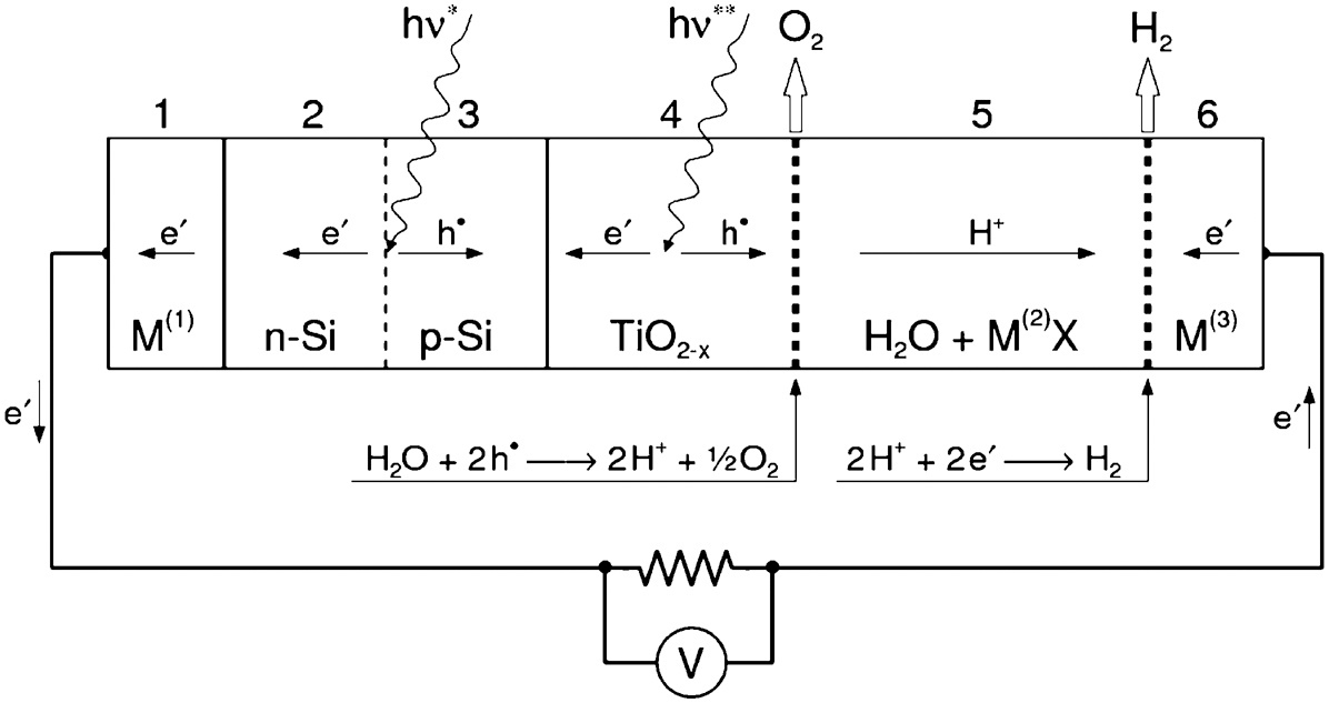
The electrochemical chain of the PEC reported by Morisaki et al. 49
While the idea of the cell of Morisaki et al. is outstanding, its ECE was relatively low because of limited charge transfer within the chain. High ECE (18%) was reported for a hybrid system reported by Peharz et al. 50
High ECE may be achieved for PECs equipped with two photoelectrodes, if these are resistant to corrosion in water. 51,52 Then, the light is collected by two electrodes.
Photoelectrochemical cell with single photoelectrode
The first approach is a PEC formed from a single photoelectrode with the band gap optimised for water splitting. Its electrochemical chain is represented in Fig. 11.
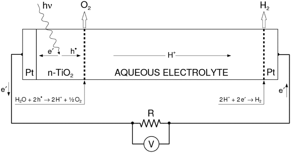
The photoelectrochemical chain of PEC involving n-TiO2 as photoanode and platinum as cathode
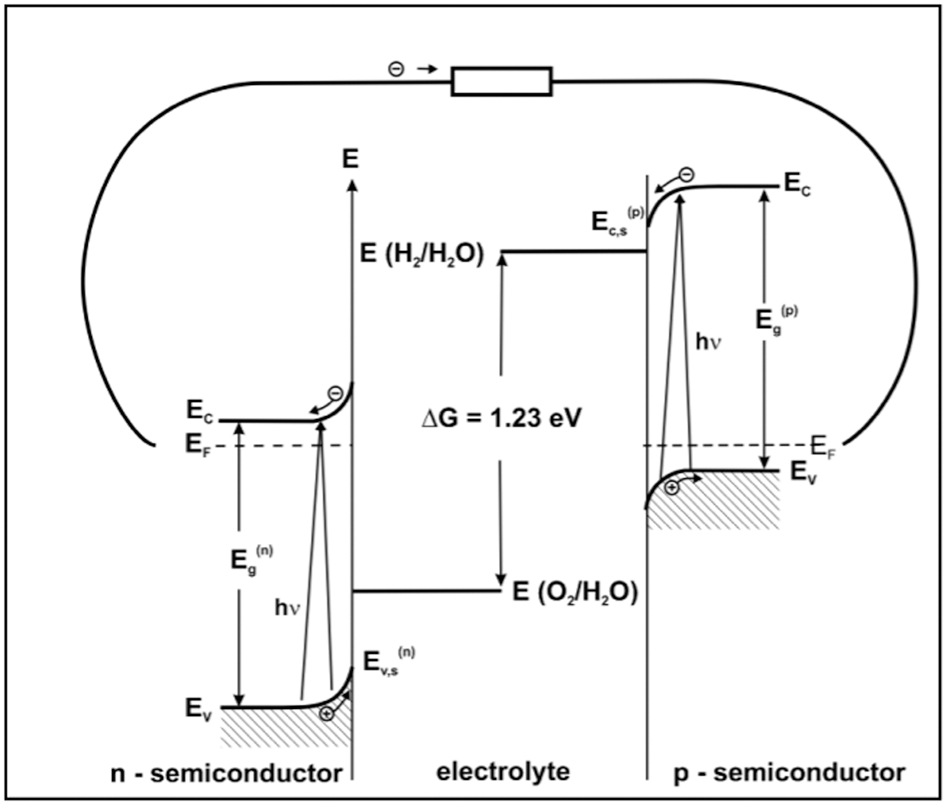
Alternative examples of PECs equipped with a single photoelectrode, formed of POSs, such as n-type α-Fe2O3, BiVO4 and p-type Cu2O, are shown in Fig. 12 illustrating the positions of the valence and conduction bands related to the electrochemical redox potentials for water oxidation and proton reduction. 53
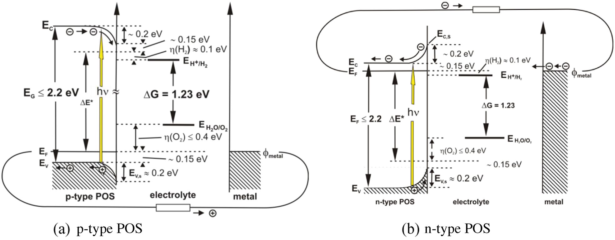
Position of the valence and conduction band of a p-type and n-type POS, respectively, related to the redox potentials H2/H+ and H2O/O2. Taking into account band bending and overpotentials, a band gap of at least 2·2 eV is needed 55
Photoelectrochemical cell with two photoelectrodes
A substantial increase in solar energy conversion may be achieved when the PEC is equipped with two, instead of one, photoelectrodes. In this solution, the light energy, which is collected by two photoelectrodes, contributes to the light-induced voltage. Water splitting may then be achieved without application of an external bias voltage.
Typical potentials need to be in the range 1·6–1·8 V at current densities of 5 mA cm−2≤I≤10 mA cm−2. 54 Figure 13 provides a visualisation of the energetic conditions required to realise such a device. Best efficiencies might be obtained using a transparent conductive substrate for one of the POSs layers (back-side illumination), while the counter electrode is illuminated via the electrolyte.
The reaction of water splitting, represented by equilibrium (3), takes place when the PEC’s electromotive force (EMF) is E = 1·23 V. However, effective water splitting for PECs with one photoelectrode usually requires application of a bias voltage. This is not the case when the PEC is powered by two photoelectrodes. Nozik 52 reported the performance of three types of PECs, in terms of photocurrent versus bias voltage, namely:
PEC equipped with two photoelectrodes involving n-TiO2 (photoanode) and p-GaP (photocathode),
PEC formed of n-GaP (photoanode) and Pt (cathode), and
PEC formed of Pt (anode) and p-GaP (photocathode).
It has been shown that only the PEC formed from two photoelectrodes results in water splitting without the need for an external bias. According to Nozik, 52 the theoretical ECE of such PEC is 45%. However, the p-type materials so far studied as photocathodes (p-GaP and p-InP) exhibit fast photocorrosion in aqueous environments leading to the deterioration of the PEC performance. 52 This will not be the case for the PEC, where both the photoanode and photocathode are made of TiO2.
Hybrid systems
Using a PV hybrid system, where the transparent front and opaque back contact of a thin film solar cell device is in direct contact with an aqueous electrolyte, decouples the PV system from the electrochemical system (see Fig. 14). The charge carrier barriers at the electrode/electrolyte interface can be lowered by using transition metal oxides such as MnOx, NiOx and CoOx and their solid solutions as dark catalysts. Defect chemistry at the oxide/electrolyte interphase might play an important role for such catalysts. 53
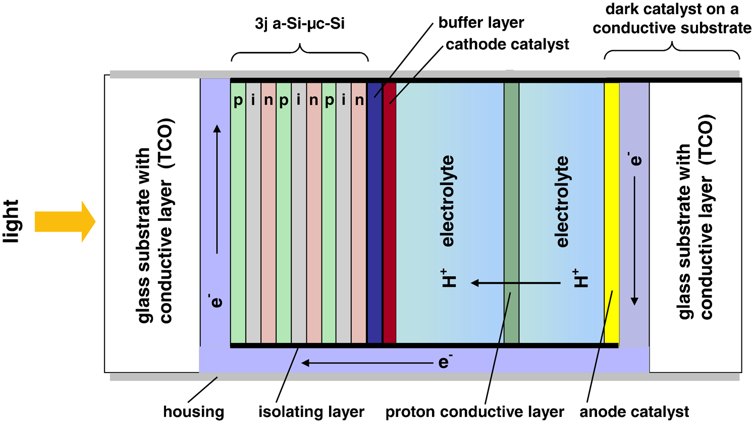
In the cross-section of this water splitting device, a triple junction a-Si/μc-Si thin silicon solar cell is shown. Since the PV cell is illuminated via the glass substrate and the transparent front contact, the electrochemical part is separated from the PV part by a conductive back contact (buffer layer and cathode catalyst). Hydrogen is formed at this photoactive cathode, while oxygen is evolved at the dark anode. The back contact and dark electrode have to be functionalised by suitable catalysts 55
Triple junction cells
State of the art triple junction silicon thin film solar cells (3j a-Si/μc-Si solar cells) possess the capability to generate a photovoltage of 1·8 V at the maximum power point and current density of >5 mA cm−2. However, a more economic version can be realised by combining a POSs with an easier to fabricate tandem junction Si thin film solar cell (2j a-Si/μc-Si solar cell) and the POS BiVO4. 55,56 In Fig. 15, a special geometry is displayed using a 2j Si thin film cell. Both sides of a TCO glass substrate are used, to deposit on one side a POS and on the other a 2j Si solar cells structure. Since the POS is acting as a photo anode and should have a higher band gap than the cathode, POS’ layers such as n-type α-Fe2O3, n-type BiVO4 and n-type TaON can be used. For lower overvoltages, the POS and the 2j Si solar cell back contacts should be provided by catalytically active particles.
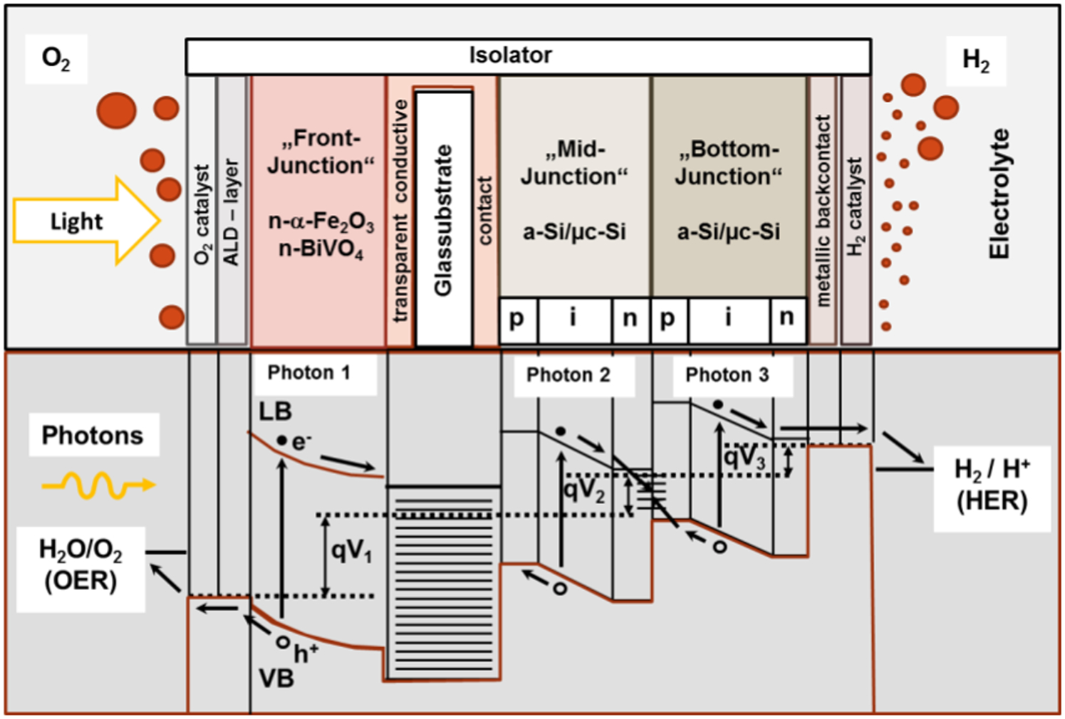
The upper part of the schematic shows a tandem junction thin film amorphous (a-Si), microcrystalline (μc-Si) silicon solar cell deposited on a glass substrate which is covered by a transparent conductive oxide layer. The water splitting device is illuminated via a POSs layer, the surface of which is functionalised by an oxygen evolving catalyst. While the oxygen evolution reaction is taking place at the anode side, hydrogen evolution happens at the metallic back contact equipped with a related catalyst. The lower part of the figure displays the band structure of the device. The harvested photovoltage is because of the splitting of the Fermi and quasi-Fermi level assigned as qV 1 – qV 3 in the three PV layer units. The band gaps of the three units decreases starting from the highest in case of the POSs and the lowest close to the back contact to absorb a high fraction of incident solar light (after Miller et al. 56 )
For all the systems described above, transition metal oxides are required. At present, no POSs can be prepared that can generate a current density of at least 10 mA cm−2 required for practical applications. During the last decade, remarkable success has been made by doping and defect control of α-Fe2O3 and BiVO4. 55,98–99 The latter currently shows the highest current density of 4 mA cm−2 measured at a pH 7 after deposition of a CoOx layer as co-catalyst. 54 The generically small carrier mobility and charge carrier lifetimes could be dramatically improved by tailoring the defect chemistry of the POS. Further improvements can be expected by designing a nano-architecture of the light absorbing films. In addition, doping gradients and modification of the surface defect chemistry should lead to improved POS performance. It is here that the enormous knowledge obtained from TiO2 could be transferred to improve these novel POSs.
Research strategy in the development of POSs for solar energy conversion
The strategy to develop POSs requires the KPPs to be initially identified and then optimised in order to achieve optimal performance and the related ECE. The performance of POSs is strongly influenced by a number of properties, including bulk- and surface-related properties, some of which are discussed here.
Electrical properties
The performance of a POS is determined by the semiconducting properties and the related defect disorder. 7–9 The electrical properties can be determined by measurements of the electrical conductivity (EC), TP and WF. However, such data are only well defined at elevated temperature corresponding to gas/solid equilibrium conditions. Such data have consequently been used in the derivation of defect disorder diagrams, which plot the concentration of defects as a function of oxygen activity. Figure 6 represents the defect disorder diagram for pure TiO2. 7–9
Electrical conductivity
The electrical conductivity measurements of metal oxides at elevated temperatures are commonly used in the determination of the effect of oxygen activity on concentration of electronic charge carriers. Such interpretation of the dependence requires to assume that the mobility term is independent of oxygen activity. 20 Electrical conductivity measurements may also be used to monitor the electrical properties of oxides during processing at elevated temperatures. 20 The dependence between the electrical conductivity and oxygen activity may be used to determine defect disorder models. 20
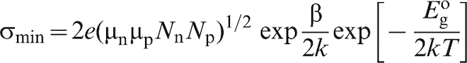
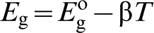
For amphoteric semiconductors such as TiO2, the band gap can be estimated from the temperature dependence of the minimum in electrical conductivity
57
Thermoelectric power
Thermoelectric power is the electrical property related to the electrical potential, which is formed along the temperature gradient. The TP for n-type materials is dependent on the concentration of electrons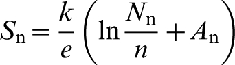
Work function
Information about the semiconducting properties of the surface layer may be obtained by WF measurements. 9,26 Changes in the WF are reflective of changes in the surface layer and its defect disorder. Work function measurements at elevated temperatures may be used for the determination of defect disorder of the outermost surface layer and the reaction kinetics at and in this layer. The WF changes of TiO2 during oxidation and reduction at 1073 K are illustrated in Fig. 16. 10
The work function (WF) changes during oxidation and reduction of TiO2 at elevated temperatures 10
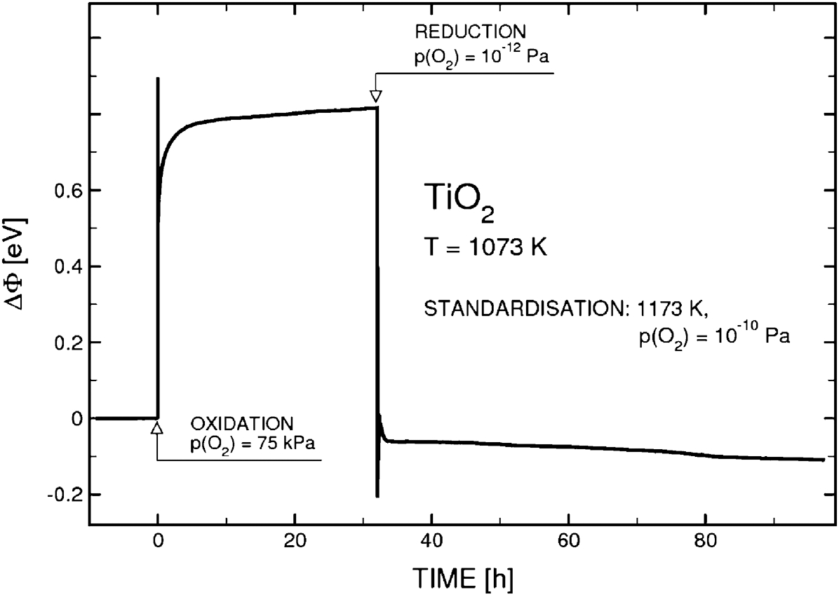
The picture is entirely different at room temperature (Fig. 17) 26 when the chemical reactions are markedly slower. In the latter case, the fast WF changes during oxidation are reflective of oxygen chemisorption and the subsequent slow changes are determined by oxygen incorporation into the TiO2 lattice. The latter process becomes extremely slow.
Work function changes of TiO2 during oxidation at room temperature showing the ranges related to oxygen chemisorptions and oxygen incorporation 26
Surface photovoltage
The effect of light, of controlled energy, on the surface charge of a POS may be monitored by measurements of the surface photovoltage (SPV). 58,59 Changes in the SPV are reflective of surface photoreactivity with the adsorbed species such as water and its decomposition products, including oxygen and hydrogen.
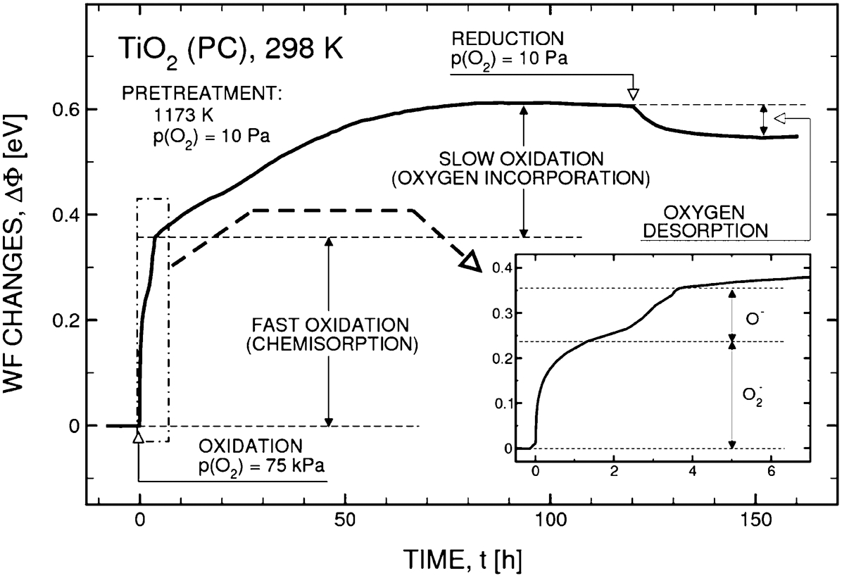
The SPV is extremely sensitive to the behaviour of surface and bulk states close to the surface of a POS, which change as a function of photon energy, temperature and gas pressure. 59 The key components of a instrument to measure the SPV are illustrated in Fig. 18.
Schematic of the set-up used to measure surface photovoltage of a photosensitive oxide semiconductor
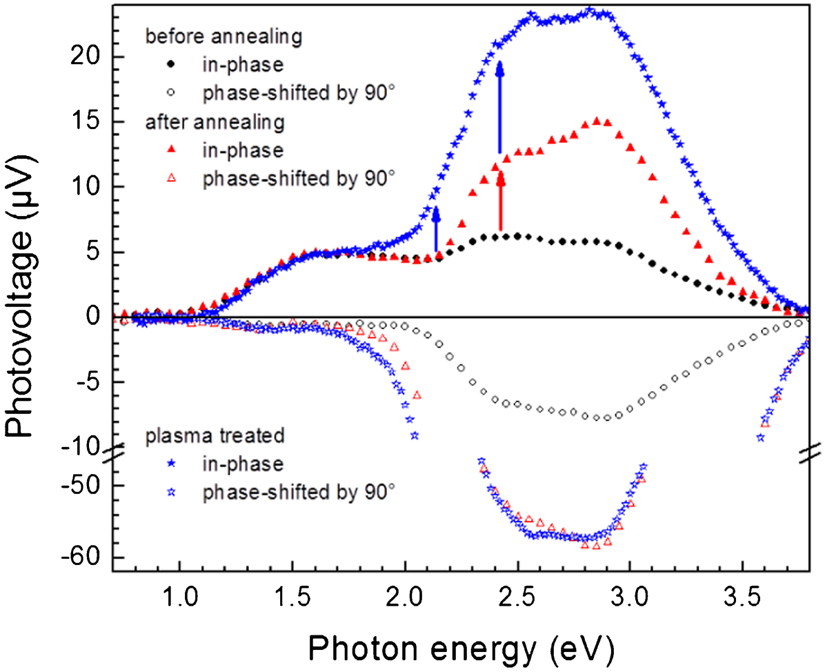
Surface photovoltage (SPV) curves of an n-type α-Fe2O3 (haematite) layer deposited by sol–gel method before and after heat treatment. The enhanced SPV signals after annealing of the haematite layer correspond to an increased activity as a photoanode in water oxidation. Black dots represent the SPV of the film as prepared, red triangles after annealing at 550°C in air and blue stars after treatment in an oxygen plasma at 800°C. The increase in SPV at photon energies above 1 eV in the upper part of the graph can be explained by states in the band gap or surface states of the POSs film. The increase above 2 eV is explained by a band to band transition of electrons in the oxide. From the lower part of the graph, conclusions can be met on the recombination velocity of surface states and bulk properties 58
Reflectance spectroscopy
It has been commonly assumed that the most critical property of oxide semiconductors is the band gap. Reducing the band gap of TiO2-based systems to below 3 eV (rutile) will enhance the absorption of light.
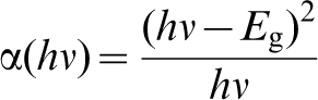
Band gap may be estimated from reflectance spectra measured over suitable energies. Knowledge of electronic transitions between the valence band and the conduction band is needed in order to select the appropriate formalism for direct and indirect transitions, respectively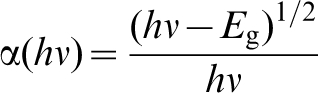
Nanotechnology
Awareness is growing that nanotechnology may lead to the formation of systems with unique properties. 60 For example, Fig. 20 shows the effect of oxygen activity on the electrical conductivity of nanostructured TiO2 compared to that of single crystal TiO2. 9 The difference between the two is substantial in terms of the absolute value of EC, its dependence on oxygen activity and the n-p transition point.
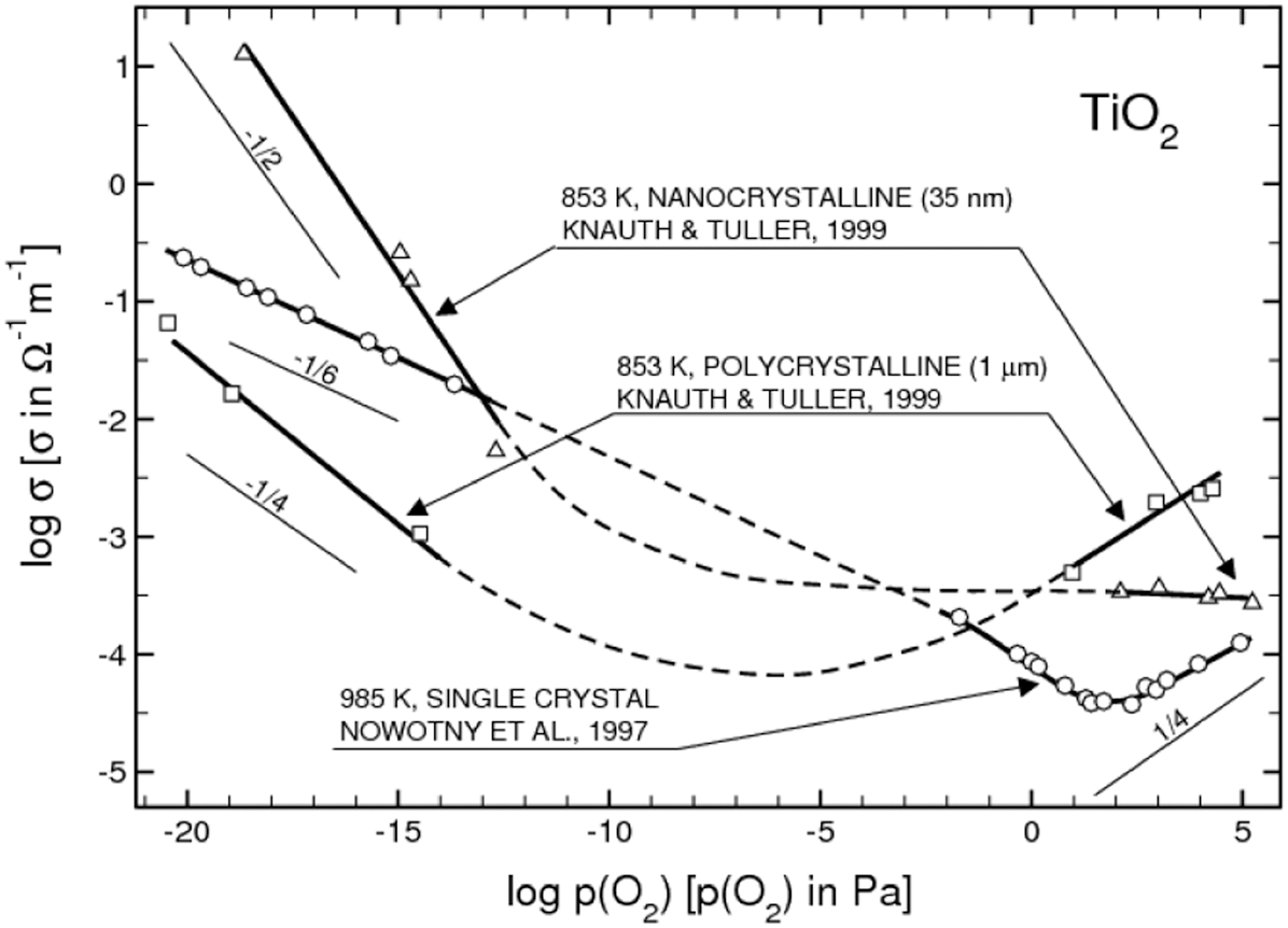
Effect of oxygen on the electrical conductivity of TiO2 specimens, including a single crystal and nano-dimensional specimen 9
There has been an accumulation of data showing that reduction of size, to the level of nanometres, results in the development of outstanding properties, which are not displayed in the bulk phase. These properties are determined by the shape and size of the nanoelements, such as needles, plates and tubes. Nanotubes of TiO2 show promising photocatalytic properties. 60
The use of anodised TiO2 nanotubes as a component in dye-sensitised solar cells, as well as in water oxidation cells and water treatment applications, has attracted significant scientific interest. Titania nanotubes are synthesised by anodisation of titanium in fluoride-containing electrolytes resulting in nanotubes that are aligned perpendicular to the substrate surface. This structure provides significantly increased surface area which enhances the photocatalytic properties of titania and reduces the electron diffusion paths to the external circuit in dye-sensitised solar cells.
The process used to prepare TiO2 nanotubes, potentiostatic anodisation, is similar to that used to prepare porous alumina.
61–64
In the first step of the anodisation process, the titanium surface is electrochemically oxidised to form an amorphous and compact layer of TiO2 on the titanium surface
65–68

The electrolyte typically contains 0·1M HF or NH4F which provide fluoride ions that complex with Ti4+, as illustrated by equation (20), and dissolve TiO2 as shown in equation (21)

The formation of nanotubes starts with pitting of the oxide layer, which provides preferential locations for the field-assisted chemical dissolution of titania by fluoride ions, as shown in equations (21) and (22). 64–68 Nanotubes are formed as the pits are chemically dissolved into the oxide layer and deepen to form the inner surface of the nanotubes. The pits provide the least resistive route for the current; therefore, the high dissolution rate forms the inside of the tubes from the pits. In order to synthesise highly ordered nanotubes, the first array of nanotubes is removed from the titanium foil leaving indentations that facilitate pitting during re-anodisation. 69
After the anodisation process, the titania nanotubes are still amorphous and thermal annealing is necessary to transform them into a crystalline state. As the nanotubes tend to collapse, as a result of sintering, at temperature above 700°C, the nanotubes are annealed at about 450°C resulting in the crystallisation of the anatase phase, or at slightly higher temperatures, yielding a mixture of both anatase and rutile. The growth and morphology of the titania nanotubes can be controlled by the parameters including the time of anodisation, voltage of the anodisation process, chemistry of the electrolyte, temperature of the electrolyte during the process, and surface roughness of the titanium precursor (Fig. 21). 69 So far, titania nanotubes of up to 1 mm length have been produced. Such long nanotubes have shown limited use in solar energy applications probably because of an abundance of defects in the material. 68 Nanotubes with a length of up to 20 μm have been shown to have the best performance for solar energy applications. 68
Schematic diagram of back-side illuminated nanotube array (on foil) dye solar cell. Reproduced with permission from Ref. 69.© 2006 Elsevier
A number of designs for titania nanotube based dye-sensitised solar cells have been proposed. Leaving the titania nanotubes on the, not completely consumed, titanium substrate results in an opaque layer in the solar cell that allows light to enter the sensitised titania nanotube array from one side only. This design is less efficient, although the remaining titanium substrate can easily be used as an electrode. When removed from the opaque titanium substrate, the nanotube array can be directly connected with transparent conducting oxides. Accordingly, light can immediately reach the sensitised titania nanotubes without being reflected or adsorbed by the counter electrode and the electrolyte.
Computational approach
Computational methods can be used to predict effects such as a tendency of certain lattice species to segregate to the surface, the resulting enrichment of the surface layer and the effect of that enrichment on the local properties. 70–75 As a consequence, these methods can be used to guide the selection of elements to be added to POSs as solid solutions.
The key problem in the selection of processing condition involving solid-state reactions, such as time and temperature required, is knowledge of the diffusion rate of specific elements in the oxide matrix. Computational methods can be used for predicting the diffusion rate and, in the case of oxides, to determine the effect of concentration of point defects on the diffusion rates.
The effect of doping on semiconducting properties depends on the ionisation energy of the donor- and acceptor-type centres formed as a result of doping. Knowledge of this is critical in the selection of the optimal ranges of doping. These data can be determined using theoretical methods.
Surface properties
Surface properties of metal oxides are different from those of the bulk phase as a result of segregation. The difference in both composition and structure may be substantial. TiO2 is not an exception. An extensive overview on surface properties of TiO2 by Diebold 76 is a prominent example of the substantial differences between the bulk phase and the surface layer in terms of chemical composition, structure and the associated properties. It seems that the applied properties of TiO2 are closely related to the difference between the two.
Awareness is growing that a wide range of properties are displayed by the bulk phase of TiO2 which are determined by defect disorder that is profoundly influenced by oxygen activity and the content of extrinsic contaminations. 9 There has been an accumulation of data showing that the range of surface structural and compositional alternatives is much larger. Research is required to understand the effect of surface processing on properties and to assess the combinations between the two that are optimised in order to exhibit maximised performance.
Recent studies of Tao et al. 37 have shown that the outermost surface layer of pure TiO2 (rutile) has a local band gap of 2·1 eV, while band gap in the bulk phase is 3·2 eV. This difference is likely related to the effect of surface energy on structural deformation. Besides the effect of the band gap, which has an impact on light absorption, the surface reactivity is strongly influenced by the Fermi level. 9 The latter determines the reactivity-related charge transfer.
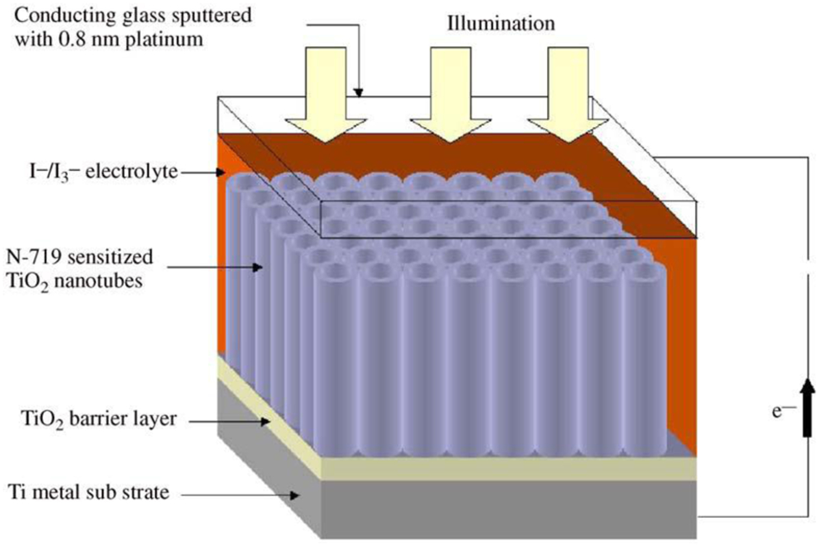
The phenomena of adsorption and segregation can have a significant effect on surface properties. The effect of segregation on surface versus bulk composition of In-doped TiO2 is shown in Fig. 22, 32 which shows that segregation strongly depends on oxygen activity. As seen, the effect is so substantial that segregation may be used as a method to control the surface properties.
SIMS depth profile obtained for polycrystalline indium-doped TiO2 before annealing (as-polished reference), and after annealing at 1273 K for 24 h in a gas phase of p(O2) = 75 kPa and 10 Pa 32
Application of nuclear techniques in processing and characterisation
Specific attributes of nuclear techniques
This section provides a brief overview of specific nuclear techniques suitable for characterisation and modification of POS materials. The nuclear techniques offer a wide range of unique approaches to characterise the bulk and surface properties of POSs and to establish the effect of modification of these on photoelectrochemical response. The techniques include: 77–97
Oxygen exchange: This technique may be used to determine the oxygen transport kinetics using oxygen isotope as a tracer.
Implantation: This technique allows controlled modification of surface and sub-surface compositions as well as growth of nano- and micro-structures.
Nuclear reaction analysis: This may be used for depth profiling of light elements.
Elastic recoil detection analysis: This can be used for the determination of the chemical composition in surface and near-surface layers.
Rutherford backscattering analysis: This can be used for chemical analysis of the surface and near-surface layers.
Proton-induced X-ray emission: This technique offers quantitative chemical analysis of a wide range of elements at the parts per million level.
Positron annihilation spectroscopy: This may be used for the determination of the concentration and space distribution of cation vacancies in oxides.
Formation of isotopic thin films: This technique may be used for growth of thin films involving specific isotopes and/or radio-isotopes.
Isotopic exchange kinetics: This may be used to determine the mass transport kinetics of specific lattice elements.
The nuclear techniques described above have the potential to provide unique insight into the properties of POSs and to monitor the effects of modification in order to achieve desired performance.
Intensive research aimed at the development of solar cells for the production of hydrogen fuel by photoelectrochemical water splitting is continuing, but the commercialisation of such solar cells, PECs, requires that the efficiency of the conversion of solar energy into the chemical energy for water splitting needs to be further improved to make this economically viable.
The focus of this section is on nuclear techniques, and in particular, their specific application in the characterisation of surface versus bulk chemical composition and microstructure as well as their modification capabilities in order to optimise the KPPs.
A wide range of techniques can be used to modify the chemical composition of POSs leading to the formation of solid solutions. The obvious limitation of this approach is determined by the properties of specific structures that are thermodynamically stable and the related solubility limits. Application of nuclear techniques offers an approach to overcome these limits through ion implantation. It has been established that implantation and post-implantation temperature treatment allows modification of both microstructure and chemical composition in a controlled manner, leading to modification of the electronic structure and the related semiconducting properties.
In addition, the use of ion beams offers the possibility depositing isotopic thin films that may exhibit outstanding properties. The deposition of isotopic thin films offers a unique approach in formation of the outermost surface layer with enhanced properties that are needed to achieve maximised performance. This approach may be used for tuning the local electronic structure and the charge transport to the level that is needed to maximise light absorption and light-induced reactivity with water.
The most commonly applied nuclear technique used for the modification of materials properties is ion implantation. While this technique is sometimes referred to as doping, the effect of this kind of doping is entirely different from that achieved by the doping using chemical processing procedures. The main difference is that it is a non-equilibrium process, it is limited to the surface layers and it is usually associated with structural damage. Post-implantation temperature treatments may be used to recover some of the damage and to diffuse or to coalesce the implanted ions, corresponding to the local solubility limit. Proton-induced X-ray emission (PIXE) may be used for very precise chemical analysis, including the determination of impurities, with the maximum sensitivity at parts per million level around Z = 26 (Fe). Rutherford backscattering offers chemical analysis for surface and near-surface layer, and depth profile of elements, and is most suited to heavy elements imbedded in light matrices. Nuclear reaction analysis (NRA) may be used for determination of chemical composition and depth profile of light elements, such as hydrogen. Positron annihilation lifetime spectroscopy (PALS) allows the determination of structural defects, such as voids (agglomerations of vacancies) and single vacancies. Isotopic oxygen exchange has been commonly used in the determination of the kinetics of oxygen mobility the oxide lattice.
Oxygen exchange kinetics
This technique may be applied for better understanding of the oxygen reduction reaction (ORR). A novel approach using oxygen-isotope exchange, called isothermal isotope exchange (IIE), has been developed to extract ORR rate coefficients and mechanisms. 77 An example of 18 O exchange is shown in Fig. 23 demonstrating an ability to distinguish surface oxygen dissociation and incorporation into the lattice. Moreover, this can be used to determine catalytic effects of surface decoration 78 and heterogeneous mixtures of oxides. Integration of these heterogeneous catalysis techniques with electroanalytical techniques, such as electrochemical impedance spectroscopy (EIS) and cyclic voltammetry will provide direct correlation between kinetic mechanisms and cell polarisation.
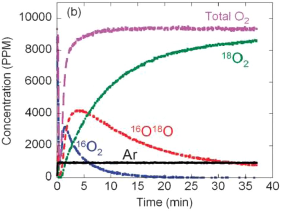
Isothermal oxygen-isotope exchange of LaFeO3, 16O2 is from bulk lattice, 18O2 is gas phase, and 16O18O is surface combined scrambled isotope product 79
The oxygen-isotope exchange technique is a powerful combination of isotope diffusion and isotope depth profile characterisation, and it allows for diffusion kinetics to be determined for specific markers in various materials. It makes use of isotope-specific nuclear reactions capable to distinguish subtle variations in concentrations.
For the purpose of understanding, the TiO2 surface properties, partial replacement of 16O with 18O, or the use of D2 16O, or D2 18O instead of H2 16O may offer advantages in monitoring surface adsorption of water.
For example, the bridging oxygen in Fig. 24, removed by ion bombardment or by thermal treatment, may be replaced by 18O instead of 16O, from a gas phase or from H2 18O. Surface and sub-surface 18O can then be detected by elastic recoil detection analysis (ERDA) with low energy Ne+ as projectile, or by the use of specific nuclear reactions such as 18O(p, α)15N using 845 keV proton irradiation.
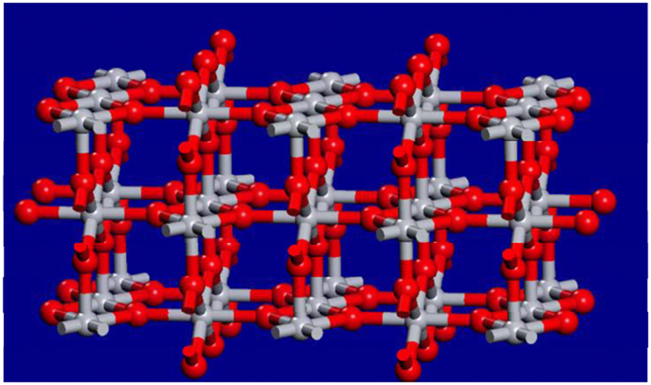
Schematic representation of defect-free TiO2 (110) surface
Implantation
Implantation is the process of bombarding the solid with specific ions, which possess the kinetic energy that is required to penetrate the surface and come to rest at a particular depth inside the target (crystalline or amorphous). In this process, the original chemical composition is changed and some atoms of the crystal lattice will be recoiled from their equilibrium position. Therefore, implantation cannot be considered as doping in terms of the formation of solid solutions that can be obtained using either solid-state reactions or soft chemistry routes. Implantation results in the formation of systems that are remote from thermodynamic equilibrium. The properties of implanted solids depend on the selected ions and their energy used for implantation. As a result, thermodynamics cannot be applied to describe the properties of solids formed by implantation. However, the post-implantation annealing may be used to gradually transfer the system from its non-equilibrium state to a system that can be equilibrated at the local atomic level. In this process, the implanted ions may diffuse inside the target or may diffuse and coalesce into nanoparticles, under the target surface or on the surface. 80 Therefore, the post-implantation annealing process may be used to form systems that are partially equilibrated, and which present characteristic properties related to both implantation and chemical doping.
Ions of most elements, and of some molecular species, can be implanted at both low (few keV) and medium energy (few MeV). Ion implantation is a very versatile and a powerful tool for surface and near-surface modifications of materials mostly because this is a non-equilibrium technique, and thus it can be used to implant any ion in any matrix. The choice of energy is a function of the mass of implanted ion, the required implantation depth and the target properties. For a particular ion, the lower the energy, the shallower the implantation depth, but below a specific threshold energy, the ion is no longer able to penetrate the energy surface barrier of the target, and comes to rest on the target surface. For some ion-energy-target combinations, this results in sputtering of target atoms, associated with surface damage. If the ion energy is further reduced, it may result in a deposition process. At the higher end of implantation energy, sputtering of the target surface may be the dominant process. Implantation offers precise control of composition and when it is carried out through masking or with a focused ion beam, it also offers precise control of location on the surface of the sample.
A variation of this technique, called ‘micro-implantation’, is achieved when the ion beam is focused down to a micrometre-size spot. If the ion current is sufficiently high, for some target materials this leads to micro-implantation or micro-sputtering and can be used to create implanted or damaged islands, or to ‘write’ complex shapes on the surfaces. 81
There are numerous examples of the use of ion implantation for materials, such as semiconductors, corrosion resistant materials, polymers, glasses, etc. In the case of oxide semiconductors, implantation offers the capability to change the surface composition and defect disorder. In particular for TiO2-based POSs, shallow implantation is one of the few ways to control the surface and sub-surface doping. 82 This leads to controlled changes in chemical composition at the surface and sub-surface regions, with the direct effect of electronic structure modifications. In addition, surface and sub-surface doping can lead to nanometre cluster formation on the surfaces and the enhancement of plasmonic effects.
In many cases, photocatalytic materials obtained by ion implantation are called second generation photocatalytic materials. In the case of thin films of polycrystalline, TiO2 made by ion cluster beam (ICB) on glass, 83,84 and implanted by V+, Cr+, Mn+, and Fe+, at 150 keV and a dose of 1016 and 6×1016 cm−2, the UV-VIS transmittance show a shift towards higher wavelength with the increase of implanted dose. XAFS indicated the replacement of Ti4+ by V3+, V4+, and ab initio DFT calculation showed a mixture of Ti(d), V(d) and O(d) orbitals, which suggest an explanation for the red shift.
In a similar study, 85 Cr and V ions implanted in TiO2 thin film show two to three times higher photocatalytic activity than the analogous non-implanted material, but the film thickness and the substrate temperature during the film deposition play a critical role in UV-VIS absorption. In the case of Cr implantation, it was shown that it also led to a decrease in the band gap and to absorption of visible light by TiO2. It was concluded that implanted Cr does not form recombination centres unlike chemically doped Cr. Also, V, Mn, Ni, Ar, Mg, Ti, and Fe were implanted in TiO2, and the red shift achieved increased in the following order: V>Cr>Mn>Fe> Ni, after annealing at 723–823 K in O2. Molecular orbital calculations showed that V3+, V4+, and V5+ substitute for octahedral Ti4+, and therefore Ti(d) and implanted ion-metal (d) orbital mixing led to narrowing of the band gap. Preliminary investigations show that ion implantation is advantageous as compared to other semiconductors and dye sensitised materials in which the e− mediator and sacrificial agents are necessary. This is not the case for implanted TiO2.
In the same study, 85 polycrystalline TiO2 and WO3, loaded with metals (Pt, Au, Pd, Rh, Ni, Cu, and Ag) and/or doped with metal ions (Fe, Mo, Ru, Os, Re, V, and Rh) lead to an increased photocatalytic activity. Also, out of a range of elements (La, Ce, Er, Pr, Gd, Nd, and Sm), Gd was the best in increasing the photocatalytic activity. Doping with Be at near the surface is beneficial, but when Be was implanted deeper the benefit is lost. In the case of WO3, doping with Ni achieved better photocatalytic activity than doping with Fe, Co, Cu, Zn, and Mn. It was shown that Cu, Mn and Fe can trap both e− and h+. Anion doping of polycrystalline TiO2 with N, C, F, and S can also narrow the BG, and is less likely to form recombination centres (unlike metal ions), and so be more effective. C and P were less effective as the introduced states were too deep, and photo-generated charge carriers were difficult to be transferred to the surface. Sulphur has shown to provide S 3p states mixed with valence band of TiO2 by shifting upwards, with no change in the width of conduction band, and consequently narrowing the band gap. Similar behaviour was observed for N-doping.
Ion implantation is one of the most promising technologies for improving the properties of TiO2 because it allows for a high impurity filling factor, beyond the equilibrium limit of impurity, solubility, and also provide control on the nanoparticles formed at different depth levels. The anatase phase appears to be better than rutile because of native higher band bending, deeper under the surface, and with a steeper gradient, enhancing the trapping of surface holes. 86 In rutile, the e−/h+ recombination is pronounced in the bulk regions, so only a smaller fraction of holes are trapped and transferred to the surface. The low ion irradiation dose of less than 1014 cm−2 results in well dispersed implanted ions. For the dose ranging between 1015 and 1017 cm−2, the implanted ions exceed the solubility limit, and form nano-particles (NP) by nucleation and growth. Low implantation energies between 10 and 300 keV is of higher interest because of the proximity to the surface of the implanted region. Implantation with Fe, V, Cr, Mn, Co, Ni, and Cu was effective in the red shift of TiO2, while Ti, Ar, and Na was not. From XAFS, Fe3+ appears to replace Ti4+ and the same for V and Cr. Also, implanted Nb and Sn are effective for increasing the matrix conductivity, in particular Sn, which is substitutional up to ∼1 at.%, when increases conductivity very high σ = 5–30 (Ω cm)−1, compared to typical σ = 1 (Ω cm)−1, obtained by conventional doping. Implantation with Cr at room temperature increases σ from 10−13 to 10−2 (Ω cm)−1. 96
Synthesis of magnetic nano particles MNP for optic and magnetic properties by ion implantation is very attractive because the dimension and structure of the MNP can be well controlled. Au, Ag and Cu show strong surface plasmon resonance (SPR) in visible or near IR range for TiO2 implanted with 2 MeV Au at RT. Also, TiO2 implanted with 40 keV Ag at 1015–1016 cm−2 shows poly-colour photochromism and antibacterial properties. 96
Thin films of TiO2 grown by reactive magnetron sputtering to 75 nm thick, were doped by ion implantation with Au at 150 keV, and a dose between 5×10¹⁵ and 1017 cm−2. At 5×1016 cm−2, Au nanoclusters of 3–5 nm diameter by X-ray diffraction (XRD) start to form in the film at RT, and during annealing at 350°C in reduced atmosphere, the nanoclusters start to coalesce, following an Oswald ripening mechanism. When annealed at 600°C, the precipitate dimensions reach 40 nm (all by in situ XRD), and annealing above 700°C promotes the formation of two Au-rich regions, at the interface and at the surface, shown by He-RBS. 97
Rutile (110) single crystals were implanted with Er at 40, 80, 150, 200, and 350 keV, at doses of 1014, 1·5×1014, 2×10¹⁴, 1·5×1014, and 6×1014 cm−2, respectively, [100]. Some samples were annealed in Ar for 30 min at 800, 900 and 1000°C. Non-Rutherford resonant scattering/channelling with 3·05 MeV He along <110>, showed no detectable crystal damage, and Er diffuse a little above 800°C, suggesting an interstitial position [100].
Irradiation of surfaces with ions implies energy transfer from ions to the target atoms, which can lead to displacement of target atoms, associated with the formation of defects, and this process is called radiation damage. The (110) structure of rutile is shown schematically in Fig. 24, where the two characteristic positions for O (in red) are visible: the in-plane and the out-of-plane locations. Ion irradiation can more easily remove the out-of-plane (bridging) surface oxygen, forming defects, and introducing an inter-band donor state, below the Fermi level, with a Ti-3d character, leading to the formation of n-TiO2. Heat treatment in reduced oxygen partial pressure may have a similar effect.
In well defined experiments, energy loss mechanisms governing the ion-target interaction are responsible in producing point defects or defect clusters, and this defect engineering may be a useful tool in enhancing specific properties of materials, such as surface reactivity (including photocatalysis), magnetic flux pinning and others.
In the case of non-stoichiometric oxides, implantation may be used to drive the deviation from stoichiometry in the desired direction. For example, implanting the host metal cation (self-implantation) results in an increased concentration of oxygen vacancies and a decrease in the concentration of metal vacancies. However, the implantation process results in destruction of the crystal lattice. Restoration of the crystalline structure requires post-implantation annealing.
A polished polycrystalline TiO2 surface, annealed in air at 1273 K, Fig. 25, shows a clear delimitation of grain boundaries and the annealing re-construction after the polishing damage of the surface of individual grains with various orientations, indicating the re-constructed growth steps. This surface was implanted with Ti (self-implantation) and Pt ions at 50 keV and a dose of 1×10¹⁶ at cm−2, Figs. 26 and 27, respectively. As compared with Fig. 25, Fig. 26 shows fewer details of grain boundaries and growth steps. Figure 27 shows barely visible grain boundaries and no growth steps. These differences can be explained in terms of damage to the crystal lattice during ion implantation. In Fig. 28, the calculated displacement damage in displacements per atom (DPA) using a Monte-Carlo based simulation programme (stopping range of ions in matter, SRIM) is shown, 89 and it indicates that the displacement damage created by Ti is spread over a larger distance from the surface with a peak of 1·8 dpa, at 40 nm, while the damage created by Pt is higher and concentrated closer to the surface, with a peak of 4·5 dpa at 15 nm under the TiO2 surface. This suggests that the differences in the appearance of the SEM micrographs shown in Figs. 25 and 26 may be explained by the higher number of vacancies and their proximity to the surface, and represent the different degree of surface damage imparted to the TiO2 crystals surface by Ti and Pt implantation at the same energy and dose.
The SEM micrograph for pure TiO2 surface after polishing and annealing at 1273 K in air (reproduced with permission from Ref. 10. Copyright T. Bak, 2010)
The SEM micrograph for pure TiO2 surface after polishing, annealing at 1273 K in air and subsequent implantation of titanium (50 keV at a dose of 1×10¹⁶ at cm−2,); (reproduced with permission from Ref. 10. Copyright T. Bak, 2010)
The SEM micrograph for pure TiO2 surface after polishing, annealing at 1273 K in air and subsequent implantation of platinum (50 keV at a dose of 1×10¹⁶ at cm−2); (reproduced with permission from Ref. 10. Copyright T. Bak, 2010)
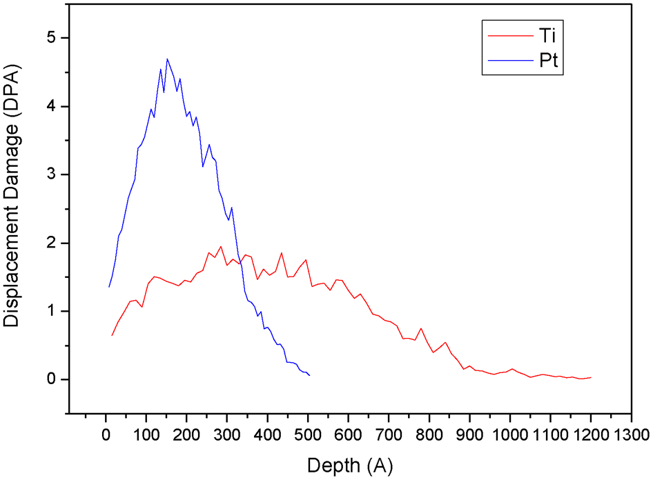
Calculated displacement damage of TiO2 by implantation of Ti and Pt with 50 keV at 1016 at cm−2 (reproduced with permission from Ref. 10. Copyright T. Bak, 2010)
Rutherford backscattering
In RBS, the probe ions of a few million electron volts, typically below the coulomb barrier for target atoms, are directed towards the sample surface at an angle between 0° and 90° relative to the sample normal. When a probe ion encounters a heavier sample atom at, or below the sample surface, a precise amount of kinetic energy will be exchanged, and the probe ion will be backscattered with a precise amount of kinetic energy, measured by a detector. This measured backscattered energy, together with the initial energy of the probe ion and the experiment geometry, are used to calculate the mass of the target atom and the location of the collision relative to the sample surface. For these reasons, RBS is a standard-less technique, and in particular H-RBS and He-RBS, is a quasi-non-destructive technique for characterising the surface, and near-surface regions. It provides the depth distribution of elements and the distribution of impurities. This can reveal additional information on the condition of interfaces and the thickness of thin films and of implanted layers. Under ideal conditions, a depth resolution of up to 0·05 ML may be achieved, for example, for Au evaporated on cleaved Mica in UHV.
The thickness of thin films determined by RBS differs from that provided by the optic-based techniques, as it measures the number of atoms per unit area of the beam and is therefore independent of the sample density. The flexibility in the choice of ions, energies and the experiment geometry offers the possibility to maximise the signal from a specific element, but the method is most suitable for analysing thin films and surfaces composed of elements heavier than the substrate or matrix, respectively. In addition, under specific circumstances, this technique offers information on multi-layers and on interfaces, such as inter-diffusion.
For TiO2 implanted with elements heavier than Ti, RBS can offer non-destructive depth distribution of the implanted ion, and therefore, the measured samples can be further used for other characterisation work, such as photocatalytic properties, thus reducing the necessity to infer identical properties for different samples characterised by the same techniques.
Elastic recoil detection analysis is another technique for the characterisation of the surface and near-surface regions, and it differs from RBS only in its experimental geometry. In ERDA, the probe ions, which are heavier than the matrix elements, are directed at the sample surface under a large angle (60–85°) from the sample normal. Thus, the heavier projectile having an adequate kinetic energy recoils the sample atoms and their energy is measured. The sample damage in this case can be higher than in RBS, but the beam flux is very small and a number of repeated examinations of the same area still provide indistinguishable results. The advantage is a complete depth resolution analysis for light, as well as for heavy elements. In particular, when the energy detection is carried out with a time-of-flight (ToF) detector, the depth resolution can be greatly enhanced to 1–10 nm. 90
Elastic recoil detection analysis and RBS can be carried out in situ or ex situ, in conjunction with ion implantation or heat treatment procedures. In Fig. 29, the result of in situ RBS on (110) TiO2 single crystal annealed in oxygen at 900°C and in Ar at 600°C is shown. This shows an unchanged oxygen stoichiometry for the as-grown and oxygen-treated sample. However, for the Ar-annealing case, the oxygen depletion is readily measurable, which allows the oxygen stoichiometry and the depth distribution of oxygen depletion in the sample under the surface to be determined.
Rutherford backscattering (RBS) with 2·5 MeV protons on ‘as-grown’ (110) TiO2 single crystal, and on the same crystal annealed in O2 at 900°C and Ar at 600°C (Copyright M. Ionescu, 2013)
Ion channelling
Ion channelling is a variation of the RBS technique, described above. The main difference consists in the direction of primary beam of probe ions, which in this case is almost exclusively He, directed along specific crystallographic directions. For single crystals, under specific orientation conditions, the direction of probe ions may be aligned with specific crystallographic channels in the sample. In that case, He probe ions can penetrate along the channel and encounter a much smaller number of the target atoms with which to collide, and thus He probes the channel integrity. If the channel is distorted as a result of the presence of interstitial atoms, or defects, the He probe ions will collide with a larger number of target atoms, and will be back scattered more often than otherwise. This may lead to the possibility of extracting additional information on the sample surface orientation, the interstitial atoms and vacancies. 91
For example, for a TiO2 single crystal implanted with an ion heavier than Ti, if channelling is carried out after ion implantation, it may reveal the type of implanted ion, its depth distribution as well as the damage that the implanted ion has created and the depth of the damage. In Fig. 30 is shown the main crystallographic directions in P42/mnm system of rutile, looking down along the [001] direction. If the single crystal surface is represented by the (110) plane, as in the previous example, then for a channelling experiment, the He probe ions will be directed along [100] direction, and the detector normal will be along [010] direction. In this configuration, the crystallographic channels parallel to these directions will be probed for distortions and interstitials.
Schematic representation of basic crystallographic directions in TiO2
In Fig. 31, the results of channelling on (100) Si implanted with Ru at various equivalent concentrations are shown, measured with 1·8 MeV He+. For comparison, the same figure also shows the He-RBS of a randomly oriented Si and of a (100) oriented Si crystal before Ru implantation. These results indicate that not only the Ru concentration and its depth distribution but also the associated Si damage peak, and its depth distribution, noting the direct correlation between the Ru concentration and the level of damage.
Channelling Rutherford backscattering (RBS) on (100) Si implanted with Ru, using 1·8 MeV He+ (Copyright M. Ionescu, 2013)
Nakamura et al. 92 reported the effect of indium implantation at 100 keV and 5×10¹⁴ and 1×1015 cm−2, at 7° from the [100] and [001] directions of TiO2 single crystal (rutile). Channelling RBS in [100] direction showed that there is only one Ti peak, but in [001] two Ti peaks were seen. This was interpreted as irradiation damage (higher energy) and the presence of In (lower energy). Annealing at 650 K gives a small recovery while annealing at 973 K gives a large recovery and a migration of In atoms towards the surface. The ψ scan around [001] and [100] indicate 88% In substitution for Ti up to 5×1014 cm−2, and 11% of In sitting in interstitial positions along c-axis at the sites (0, 0, 1/4). With increasing dose to 5×1015 cm−2, In precipitate in clusters, with 3% substituting Ti, 15% interstitial at (0, 0, 1/4) and 82% random position, but with annealing at 973 K, the In distribution was 20% substitution and 80% random. The increase of In interstitial occupancy after implantation and its disappearance after annealing suggest that In is interacting with defects resulting from implantation, which could be in the form of: indium–titanium vacancy pair; indium-Schottky defect complex; indium–oxygen divacancy complex; and indium–titanium mixed dumbbell.
Elastic recoil detection analysis
As mentioned in the RBS section, ERDA differ from RBS in its experimental geometry, with the direction of the incident probe ions and the detector normal forming a large angle (60°–85°) from the sample normal. The advantage of this configuration is that the heavy and energetic projectiles used can recoil all the sample atoms, and thus the complete sample composition, from the lightest (H) to the heaviest element present, can be determined, as well as their depth distribution, with a depth resolution between 1 and 10 nm.
In Fig. 32, the ERDA result using 82 MeV I+10 probe ions, for a LiNbO3 thin film deposited by CVD on (100) Si, and a time-of-flight (ToF) detector is shown. On the right the schematics of ERDA experimental geometry and on the left the detection result of the (ToF, energy) plane are shown.
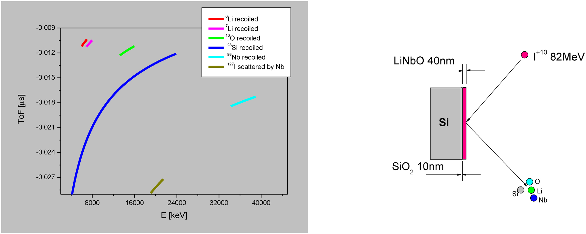
Typical (t-E) elastic recoil detection analysis (ERDA) result obtained with 82 MeV I+10 probe ions for a LiNbO3 thin film deposited on (100) Si, and a time-of-flight (ToF) detector; on right is experimental geometry (Copyright M. Ionescu, 2013)
This result indicates that the depth distribution of all elements present in the LiNbO3 film, including the Li isotopes, the thickness of the film (∼100 ML), the presence of a SiO2 film (∼6 ML thick) at the interface, and the diffusion of Nb in Si substrate.
Nuclear reaction analysis
When the energy of the probe ions is higher than the coulomb screening barrier of the target atoms, a specific nuclear reaction can be triggered between the probe ion and the target atomic nucleus. There is a large number of nuclear reactions, and specific nuclear reactions can be used for surface and near-surface characterisation, when, for example, the direct measurement of a particular element is difficult to achieve through other techniques. Light elements (up to Al) usually fall in this category, and nuclear reactions can yield prompt reaction products. In particular, nuclear reactions with narrow resonances and γ-ray products are a first choice for depth profiling of light elements, with a depth resolution of around 10 nm.
NRA can be used for both crystalline as well as for amorphous samples, and in specific cases, it can be combined with the isotopic exchange kinetics, representing a powerful combination of isotope diffusion and isotope depth profile characterisation. An example is presented in Fig. 33 of the use of the15N(H, αγ) 12C nuclear reaction for the depth profiling of hydrogen in DLC thick films. This nuclear reaction has a narrow reaction resonance of 1·8 keV, and as the energy of probe 15N ions of 6·4 MeV collide with the surface H, prompt γ photons of 4·43 MeV are created and detected. As the energy of the probe ions is increased above 6·4 MeV, they penetrate the sample surface, and start losing their kinetic energy. When this energy decreases down to 6·4 MeV, and 15N collide with another H, a new reaction is triggered and the new γ-ray photon is detected. For this nuclear reaction, the depth of analysis range from a few nanometres, up to a few hundreds of nanometres, with a depth resolution of 5–20 nm.
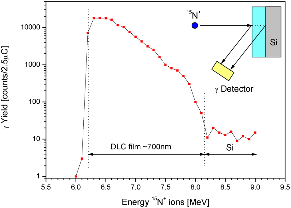
Nuclear reaction analysis (NRA) of H in DLC thick films (Copyright M. Ionescu, 2013)
Particle-induced X-ray emission
When the probe ions collide with target atoms on or under the surface, one possible consequence is the ionisation of the target atoms, and the subsequent emission of characteristic X-rays. Proton-induced X-ray emission is a surface and near-surface analysis technique, and is suitable for analysis of elements heavier than Al. The depth of analysis is dictated by the type of the sample matrix, the energy of probe ion and the type of probe ion. The analysis is usually carried out with protons between 1 and 3 MeV, but for specific samples other probe ions such as He or C may be used.
The characteristic X-rays are detected, and the quantitative analysis is achieved by a calibration procedure with known standard samples. Optimum detection sensitivity is near Fe (1 ppm), and other element sensitivities range from 1 to 100 ppm, which is about 100 times better than EDX, and is mainly because of a much lower background. For proton PIXE, the typical depth of analysis ranges from 20 to 50 μm, but the depth information is absent. 93,94
Proton-induced X-ray emission can be carried out with a broad ion beam or with a focused ion beam. In the latter case, the ion beam is focused down to micrometre, or even sub-micrometre, size and rastered over area to be analysed, which confers the additional capacity to extract spatial information on the surface distribution of a particular element, with a lateral resolution of less than 0·5 μm. In this way, surface X-ray mapping of element distribution can be measured.
Proton-induced X-ray emission is a powerful tool in determining the concentration of a wide range of secondary elements, which are added intentionally (doping) or unintentionally (impurities). Since the presence of aliovalent ions already at the level 5–10 ppm results in substantial changes in properties, the characterisation of POSs should include the determination of the impurities.
Positron annihilation lifetime spectroscopy
The positrons emitted from a radioactive source such as
22
Na can penetrate the surface of a conductor or an insulator and quickly thermalise.
A refinement of this technique consists of the use of a micro beam of pulsed positrons for enhanced lateral resolution which afford the possibility to measure both the lifetime and the Doppler broadening of the annihilation reaction, and produce 2D defect maps. 95
An example is taken from Ref. 95, where fluorine was implanted in TiO2 single crystal at 200 keV, and at doses between 1016 and 1017 cm−2, and after annealing in air at 1200°C, SIMS shows fluorine migration towards the surface. Channelling RBS with 2 MeV He shows damage, and XPS suggest F replacing O. When PALS was performed with positron energies between 0·2 and 25 keV, it measured the broadening and S parameter of the annihilation response before and after implantation and recovery annealing, which indicated the creation of vacancies. 95,96
Summary
The nuclear techniques reviewed here can offer major benefits in advancing the technology of POSs, from sample preparation to sample characterisation. They are adequate for POSs requirements of surface and near-surface modification and characterisation, and can be beneficial in tailoring the POSs properties bringing these materials closer to industrial applications.
The use of nuclear techniques requires the building and maintenance of major facilities, and therefore their cost can be high. In some cases, the need of high energies requires the use of accelerators or the use of radioactive sources. In addition, the use of nuclear techniques and facilities require specific expertise, and are subject to strict safety regulations, and these are the main reasons why these techniques are mainly concentrated at national facilities.
The nuclear techniques are frequently associated with the use of isotopes, which are required in order to distinguish the tracer particle from the background formed by the same elements.
While the nuclear techniques are frequently considered as hazardous if related to radioactivity, the present work represents an example of the application of nuclear techniques for protection of the environment through the development of a new generation of solar materials that can be used for solar cells for the production of environmentally friendly fuel and for water purification.
Education programme on sustainable energy systems (SES)
There is an urgent need to develop education programmes for training the technical staff able to work in the front line of the developing sustainable energy systems (SES), including 97
Hydrogen energy: The related technologies include hydrogen generation, hydrogen storage, hydrogen transportation, hydrogen distribution, hydrogen utilisation and hydrogen safety.
Electrochemical energy: The related technologies include fuel cells and chemical gas sensors.
Photoelectrochemical energy: The related technologies include photocatalytic water purification and photoelectrochemical water splitting.
Photovoltaic energy: The key technology in this category corresponds to PV solar cells.
The SES programme is expected to equip the technical and managerial staff with the tools required for assessment of competing technologies in terms of their economic, environmental and social aspects. The main hurdle in the development of education programmes on SES is their multidisciplinary character.
Unresolved materials challenges
Here, a range of problems, which must be resolved in the development of new semiconducting materials with enhanced performance that address the requirements of modern day technologies are considered. This section also formulates the associated questions, which must be addressed in the related R&D programme.
Cost competitiveness
The R&D efforts aim at the development of novel solar materials for high-performance energy conversion devices. The key requirement of these materials is cost competitiveness. Therefore, the research aims to develop the systems (materials and devices) that allow conversion of renewable energy at the lowest cost per unit of energy. This can be achieved either through higher conversion efficiency leading to enhanced production of energy, which should be measured in terms of the units of power, or reducing the costs of materials and solar cells. The following questions may be formulated here:
How processing costs of the existing solar materials can be reduced?
How the ECE can be enhanced through the modification of the performance-related properties?
How new photosensitive materials, which are inexpensive, can be developed?
Properties of the outermost surface layer
The reactivity and photoreactivity of oxide semiconductors are determined by the properties of the outermost surface layer. So far, little is known about the properties of this layer, including chemical composition, structure, microstructure and the related semiconducting properties, and their effect on reactivity. Therefore, the progress in the formation of systems with enhanced photocatalytic performance requires imposition of a surface layer with controlled composition, structure and reactivity. The key questions, which must be addressed to make the progress, include:
What are the surface properties required for a maximised performance?
How can the performance be optimised through manipulation of the local and collective surface properties?
What procedures allow modification of the surface properties in a controlled manner?
What role do surface defects play towards improved charge transfer between the POSs and additionally deposited co-catalyst particles?
Surface versus bulk semiconducting properties
Solar energy conversion depends on both surface and bulk properties. Maximised performance requires that the difference between the two is optimised. The reactivity at the solid/liquid interface in dark conditions is determined by surface properties. However, light-induced reactivity at this interface is profoundly influenced by the flat band potential, which depends on the concentration gradients between the surface and the bulk phase. The key questions, which must be addressed for progress, may be formulated as follows:
What is the effect of surface versus bulk properties and the related electric field on the charge transfer between oxide semiconductors and water?
How the electric field can be modified in a controlled manner in order to reduce the recombination-related energy losses?
Effect of segregation on the formation of low-dimensional surface structures
Segregation of selected lattice elements to interfaces, including the external surface, results in the formation of strong concentration gradients within the interface layer. When their concentration surpasses a certain critical value, the crystalline structure of the surface layer is deformed leading to the formation of a low-dimensional surface structure, which can exhibit unique properties. The photocatalytic performance of the TiO2-based system depends on the specific properties of the surface structure which is formed at the TiO2/H2O interface. The progress in this area requires that the following questions are addressed:
What is the effect of segregation on the formation of low-dimensional surface structures?
How can the effect of segregation be used for engineering of the chemically induced electric field?
Modifications of the outermost surface layer
Reactivity and photoreactivity are determined by the properties of the outermost surface layer and specifically, the local surface active sites, which lead to the formation of an active complex with water. Therefore, the reactivity may be optimised through the modification of these local properties, which leads to increased population of these sites. Here, the following questions may be formulated:
Which are the specific surface active sites for the formation of active complexes with water?
How can the outermost surface layer be modified in order to enhance the performance?
How stable the surface active sites are?
Mechanism and kinetics of partial and total water oxidation
Water oxidation requires the transfer of electrons from water molecules to the semiconductor. The ability of the surface to promote partial and total oxidation of water depends on the affinity of the surface to electrons. So far, little is known on the specific surface properties that are responsible for the mechanism of water oxidation. Here, the following questions may be formulated:
What is the mechanism of water oxidation?
Which specific surface properties are responsible for partial and total water oxidation?
Identification of critical properties in the development of high-performance photocatalysts
The performance of photocatalysts is determined by several KPPs that are interdependent. 7–9 It has been shown that the modification of one property results in the modification of the remaining properties. Therefore, the development of POSs with maximised performance requires a multifactorial approach in the optimisation of all KPPs. In this respect, the following questions may be formulated:
Which are the specific KPPs?
What is the effect of all KPPs on partial and total water oxidation?
What is the interdependence between the KPPs?
Identification of critical issues in the development of high-performance photoelectrodes and photocatalysts
There is an urgent need to derive theoretical models which are reflective of the relation between the specific properties and performance and which can be used in the optimisation of the performance-related properties. Such models can be used for predicting the effect of properties and performance. Robust theoretical models can be derived using the experimental data, which are well defined, reproducible and compatible. This, consequently, requires that collection of data for the specimens, which are well defined not only in terms of structure, phase relations, and non-stoichiometry but also the related defect disorder. Here, the following questions can be formulated:
How to collect the experimental data, which are well defined and reproducible?
Which properties are critical for the performance and how can these properties be determined in a reliable manner?
Surface recrystallisation
During the performance, the surface layer of POSs will recrystallise in order to assume the crystalline form that is more stable in the performance environment. Establishment of the effects leading to restructure during the performance is critical in order to minimise the adverse effects of surface recrystallisation. In particular, dopant cations, such as Ru or Nb, it is likely that the surface concentration of these, and their coordination environment, will evolve during the life time of the cell. Here, the following question can be formulated:
What is the effect of the solar cell environment on the properties of photocatalyst and photoelectrode and their performance?
Conclusions
The present work reports the progress in the development of POSs for the conversion of solar energy into the chemical energy required for partial and total water oxidation. The focus is on the processing of POSs with optimised semiconducting properties that are needed for maximised performance in the production of solar hydrogen fuel from water as the raw material. The performance is profoundly influenced by a range of the KPPs, which are related to the surface and the bulk defect-related properties. Therefore, the promising strategy in the development of high performance of POSs is the application of defect engineering in the processing of oxide materials with controlled properties that are desired for specific applications. It is shown that the electrical conductivity is the key defect-related property, which may be applied for in situ monitoring of the processing of POSs at elevated temperatures and the related charge transfers. Alternative methods, such as TP, WF and SPV measurements are shown to be crucial in the characterisation of surface versus bulk semiconducting properties of oxide semiconductors. It is also shown that the determination of the effect of segregation, leading to enrichment of the surface layer in certain lattice elements, is crucial in proper characterisation of POSs. The progress is determined by better understanding of the reactivity and photoreactivity of POSs with water and its decomposition products, oxygen and hydrogen. The present work has identified the hurdles in the development of POSs with enhanced performance and has formulated the key questions to be addressed in overcoming these hurdles.