
Abstract
Simple compression and microscopy techniques were employed to characterise the microstructural origin of the deformation behaviour of nickel base superalloy IN625 during large strain testing. The alloy exhibited a four-stage strain hardening response similar to that previously reported for low stacking fault energy face centred cubic alloys. At strains lower than about −0·06 (stage A), a falling regime of the hardening rate was observed. This stage was followed by a second stage (stage B) of slow increasing hardening rate, which was found to be coincident with the formation of Lomer–Cottrell locks. The second falling regime of strain hardening (stage C) was seen in the strain range of −0·25 to −0·65. The occurrence of this stage was attributed to the increasing ease of dislocation cross-slip with increasing strain and consequently to the decreasing Lomer–Cottrell lock efficiency in hindering dislocation movement. Beyond a strain of −0·65, a final slightly constant hardening regime (stage D) was developed. The initiation of this stage was concurrent with the onset of deformation twinning in the microstructure.
Introduction
Recent investigations on the strain hardening response of different face centred cubic (fcc) alloys have shown that the strain hardening rate–true strain plots for low stacking fault energy (SFE) polycrystalline alloys (such as Hadfield steels, 1 1,2 austenitic steels3 and a number of Co–Ni superalloys) 4 4,5 exhibit four distinct regimes of hardening. In the original paper of Asgari et al.,3 the microstructural origin of different hardening regimes was described. Deformation twining was considered by these authors to be the main origin of high hardening rates observed in a number of low SFE fcc polycrystals at room temperature. On the other hand, a recent study6 has shown that twinning may not be the sole cause of high hardening rates in low SFE fcc polycrystals. To study the microstructural origin of hardening rates in fcc polycrystals, IN625 was selected for further investigations. Wrought nickel base superalloy IN625 is widely used in aeronautical, aerospace, chemical and marine applications. The wide application of this material is mainly due to its remarkable combination of high strength, creep strength, excellent fabricability, weldability and outstanding corrosion resistance.7 Despite extensive study on the precipitation behaviour and high temperature deformation modes of this alloy, no comprehensive study has been performed to characterise the microstructural origin of room temperature deformation behaviour of this superalloy. A clear understanding of the deformation behaviour of IN625 is an essential step to exploit the full potential of this interesting superalloy and other related alloy systems. The main goals of this research have been to perform a detailed microstructural study on the deformed IN625 and to identify the micromechanisms involved in the plastic response of the material.
Experimental
Commercially drawn rods of superalloy IN625 provided by SPS Technologies, Inc. (Jenkintown, PA, USA) were used to produce the desired samples. Table 1 shows the chemical composition of the IN625 alloy used in the present study.
Chemical composition of IN625 alloy used in present study
The as received material was solution treated at 1453 K for 1 h and 973 K for 3 h to obtain a single phase solid solution with fcc structure. Cylindrical samples with diameter of ∼6·5 mm and length of 7·6 mm were prepared and tested in simple compression (up to a true strain of ∼0·7) using a computer controlled servohydraulic Instron 4208 machine. At room temperature, a constant true strain rate of −0·001 s−1 was maintained throughout the tests. The specimen ends were lubricated by Teflon spray and high pressure grease to minimise frictional effects and avoid barrelling. True stress–true strain curves were calculated from load–displacement data after correction for machine compliance. In addition, a number of samples were deformed to different strain levels for further microstructural investigation.
The selected specimens for optical microscopy (OM) were prepared by mechanical polishing the longitudinal sections of the samples followed by electrochemical etching. Electrolytic etching was carried out in a 20 oxalic acid solution at about 5–6 V using a stainless steel cathode for ∼20 s. An Olympus BX51M microscope was used for the OM studies. Foils for transmission electron microscopy (TEM) were prepared from 0·4 mm slices taken from the selected samples. Final thinning was performed using a Struers Tenupul-5 unit at 18 V and 248 K in medium containing one part perchloric acid and four parts ethanol. A Philips CM200 scanning TEM operating at 200 kV was used for the TEM studies.
Results
Mechanical response
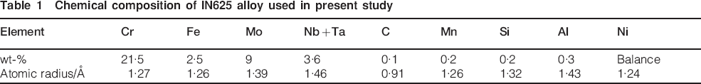
Figure 1a shows the true stress σ–true strain ϵ response of IN625 with an average grain size of 150 μm under simple compression. Strain hardening rate dσ/dϵ versus strain response was numerically calculated from the stress–strain curve and was normalised by the shear modulus G (79·4 GPa), as shown in Fig. 1b. It is seen that the strain hardening rate versus strain plot of the alloy shows four distinct stages of hardening, labelled A, B, C and D respectively. Figure 1c shows that this behaviour is in agreement with previous observations for low SFE fcc alloys. In this figure, the same normalisation procedure has been used for the all of the materials compared.
a true stress–true strain response of IN625 alloy in simple compression, b variation in normalised strain hardening rate θ/G versus true strain numerically calculated from a and c normalised strain hardening rates of some low and medium SFE fcc alloys at various true strains
At strains of lower than about −0·06 (stage A), a falling regime is observed. This stage is very similar to the dynamic recovery regime observed in copper (Fig. 1c). In comparison to copper, however, it only lasts up to very small strains. This stage is followed by a second stage of slightly increasing hardening rate (stage B). The second falling regime of strain hardening is seen in the strain range of −0·25 to −0·65 (stage C). At large strains, beyond −0·65, this stage is interrupted by a second slightly constant hardening rate (stage D). It is necessary to note that the stage D strain hardening rate is significantly higher than the strain hardening rate observed in stage IV hardening of copper (Fig. 1c).
Optical microscopy
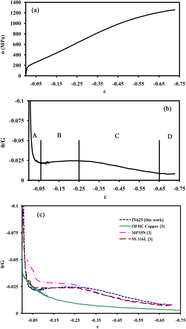
The OM of the solution treated samples revealed extensive occurrence of annealing twins and especially parallel sided twins. This feature has been recognised to be the great majority for low and medium staking fault energy alloys. The observed twins had preferential orientations within each grain (Fig. 2). The TEM studies revealed that the coherent boundaries are (111) plane. At stage A, the microstructure of the samples indicated the formation of thin and straight lines of slip.
Typical OM image of parallel sided annealing twins with preferential orientations within grain
Figure 3 shows an OM image of the sample deformed to a strain of −0·04 (corresponding to the end of stage A) taken from an area close to an annealing twin boundary. Cross-slip of dislocations is clearly seen in this micrograph.
Image (OM) from area close to annealing twin boundary in sample deformed to strain of −0·04
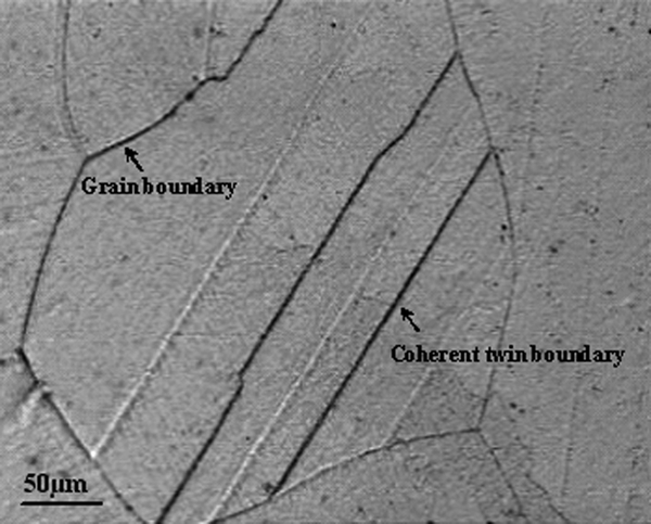
Figure 4 shows an OM image of the sample deformed to a strain of −0·25. Some deformation markings can be seen in this micrograph (as shown by the arrow). These markings have been described as deformation twins3 or dislocation pile-ups.6
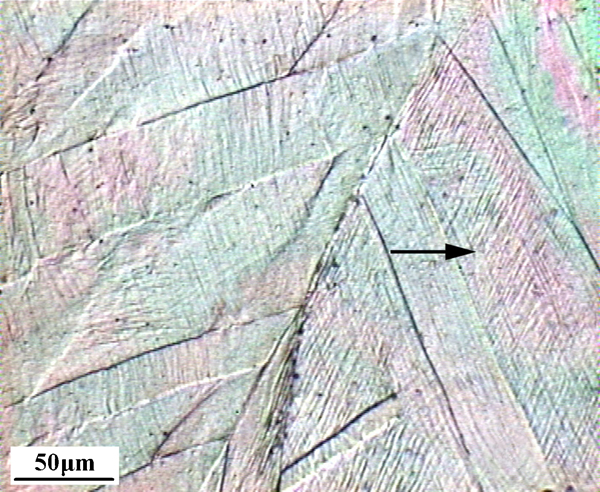
Image (OM) of deformation markings (shown by arrow) in sample deformed to strain of −0·25
Electron microscopy
At stage A, TEM studies showed no deformation twins in a large number of grains in different samples. The microstructure at this level of deformation consisted of planar arrangement of dislocations. Interestingly, at this strain, a few Lomer–Cottrell (LC) locks were also observed along the [110] direction, as shown by the arrow in Fig. 5. The LC locks can be formed in the following way.
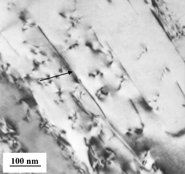
Image (TEM) of sample deformed to strain of −0·04 showing formation of LC locks along [110] direction (one lock is shown by arrow)
In most metals and alloys, perfect dislocations dissociate in their glide plane into two Shockley partials bounding a stacking fault ribbon. If two perfect dislocations gliding in different {111} plane meet at the line of the intersection of the two planes, then the leading partials repel or attract each other according to the particular direction of their Burgers vectors. Among the possible combinations, a product dislocation with Burgers vector of the form of 1/6 〈110〉 is the most favourable. This dislocation cannot glide on the intersecting planes and exerts a repulsive force on the two remaining partials. These three partials form a sessile arrangement known as LC lock.
With increasing plastic strain from −0·04 to −0·25, the density of the LC locks was increased, while no deformation twin could be found in the microstructure. Figure 6 shows a high magnification image of a region with high density of LC locks. Extensive TEM investigations showed that the deformation markings observed in Fig. 4 were not deformation twins. On the other hand, as shown in Fig. 6, a significant increase in the number of LC locks occurred at a strain of −0·25. Remarkably, even at this level of deformation, few stacking faults were observed in the microstructures.
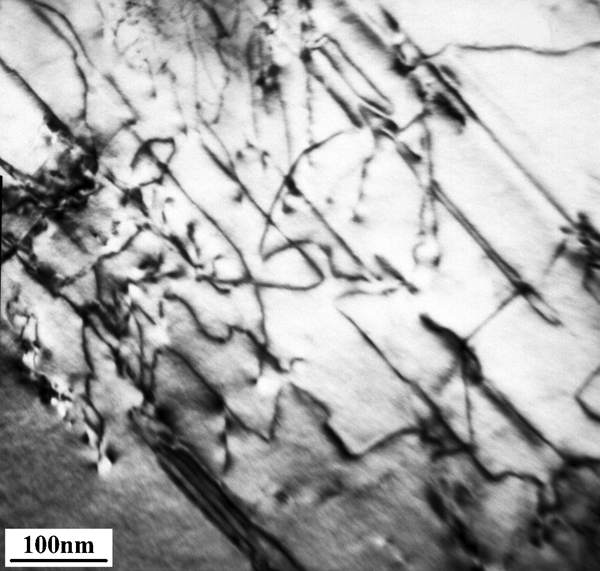
Image (TEM) of sample deformed to strain of −0·25 showing increased number of LC locks
Figure 7 shows a TEM image of the sample deformed to a strain of −0·4. At this level of deformation, the arrangement of dislocations was still planar, and the cell structure was not observed. In addition, no sign of deformation twinning was observed in the studied grains. With increasing plastic strain beyond this level, however, the planar arrangement of dislocations was gradually destroyed. Further TEM investigations showed no deformation twinning in samples deformed to strains up to −0·65. At this strain, however, the formation of intersecting twins was observed.
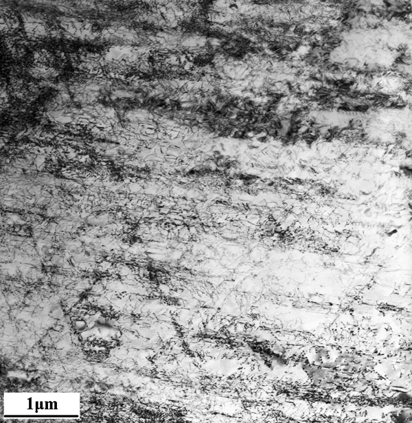
Image (TEM) of sample deformed to strain of −0·4 showing planar arrangement of dislocations
Discussion
The results presented in the present investigation reveal important aspects of deformation of IN625 alloy. Earlier studies correlate the fall in the strain hardening rate during stage A to the occurrence of cross-slip. 3 3,6 This is confirmed by our microstructural observations in the present work (e.g. Fig. 1b). In addition, a planar arrangement of dislocations was observed in the strain range of −0·04 to −0·4. The slip planarity in fcc alloys is mainly related to the following factors:
low SFE
large lattice frictional stress
short range ordering (SRO).
With the decreasing normalised SFE (γ/Gb, where γ is the SFE value, G is the shear modulus and b is the magnitude of Burgers vector), the equilibrium distance between Shockley partials increases, which makes cross-slip more difficult and promotes strain hardening rate.8 In a recent study,9 the SFE value of IN625 was measured to be ∼60 mJ m−2 from direct observation of the extended dislocation nodes and applying the theory of Brown and Thölén. This suggests that IN625 is not a low SFE alloy, which is in agreement with the lack of stacking faults on the microstructure of the deformed samples. Therefore, a low SFE cannot be the origin of dislocation planarity in the present work.
Large solute atoms, such as Mo and Nb (Table 1), create large lattice frictional stresses.10 Dissociated partials need extra energy to overcome these frictional stresses before their recombination, which is a critical step in cross-slip process.11 Extensive formation of SRO in some Ni–Cr alloys has been reported in the literature.12 In addition, heat treatment of wrought samples may facilitate SRO formation. Pass of the first Shockley partial through the ordered lattice destroys this SRO, producing some extra energy, which is thermodynamically unfavourable. Since the order is only of a short range, the following dislocations are not able to restore this order. Therefore, when a dislocation source is activated, all the dislocations prefer to slip on the same plane to minimise the imposed extra energy, which, in turn, brings about the planar configuration of dislocations.13 The presence of fairly extended multipoles and unpaired dislocations even in the microstructure of the samples deformed to larger strains (Fig. 8) suggests that lattice frictional stress and SRO are the main factors contributing to the planarity of dislocations in this alloy.
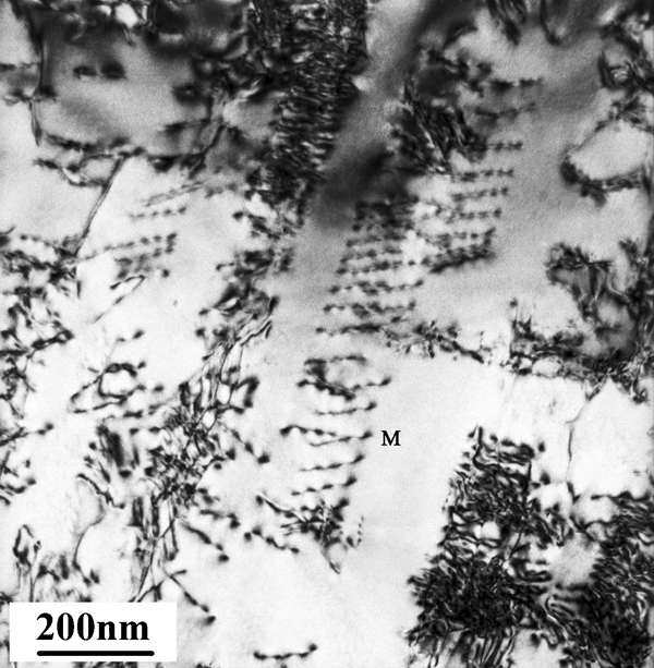
Image (TEM) of sample deformed to strain of −0·25, showing multipoles marked by M, where dislocations are not equally paired
A remarkable result of the present study is the microstructural origin of initiation of stage B. While a number of recent studies on low SFE fcc alloys 3 3,14 have correlated the onset of stage B to the formation of primary deformation twins, no deformation twin was observed in the present investigation. Interestingly, the initiation of stage B was found to coincide with the formation of LC locks (Fig. 4). We suggest that the appearance of these LC locks is responsible for the termination of stage A and the onset of stage B with slightly increasing hardening rate. These locks act as strong barriers to the glide of active dislocations on the intersecting planes, which form the lock. The planar slip of dislocations enhances the efficiency of LC locks in hindering the dislocation movement. This should stop the strain hardening rate to fall to lower values (Fig. 1b). The steady increase in strain hardening rate during stage B is related to the increased density of the piled up dislocations behind the LC locks and the increase in the number of grains containing these locks (Fig. 6).
At a strain of −0·25, the density of piled up dislocations reaches its maximum and consequently the strain hardening rate stays at its maximum. During stage C, cross-slip is the dominant deformation process. At these strain levels, partials receive enough stress to overcome the lattice frictional stress and pass the locks. In addition, at this level of stress, several sources of dislocations are activated, which push the SRO regions to collapse and provide easier cross-slip. These explain why a second falling regime of strain hardening is observed at the strain range of −0·25 to −0·65.
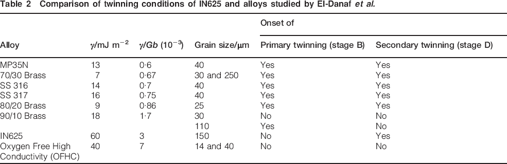
Interruption of stage C by a slightly constant hardening regime (stage D) implies the activation of a new hardening mechanism. The overlap of IN625, α-Brass and MP35N hardening values at strains larger than −0·65 (Fig. 1c) manifests the similarity of hardening mechanisms in these alloys at this stage. Our observations show that the initiation of this stage is concurrent with the onset of deformation twinning. Twin boundaries act as strong barriers against slip propagation.15–17 In essence, the formation of these deformation twins shortens the slip distances and causes the strain hardening rate to stop falling. El-Danaf et al.18 investigated the effect of SFE and grain size on deformation twinning in some low and medium SFE fcc alloys in detail. It was shown that a combination of high dislocation density and relatively large homogeneous deformation length (HDL) is necessary for twinning. The HDL is defined as the length of the region of the grain in which there is homogeneity of slip, as revealed by a set of parallel slip markings in that region. This criterion may be used to explain the reason of observing twins in IN625 at large strains.
Table 2 compares the twinning conditions of IN625 and the alloys studied by El-Danaf et al. It is observed that low SFE alloys (normalised SFE of about 0·6−0·86×10−3) with high strain hardening rate and larger HDL exhibit both primary and secondary twinning, while in 90/10 Brass (with higher normalised SFE), only primary twinning occurs in large grain size samples. This was attributed to the larger HDL under these conditions that promotes deformation twinning. The high planarity of dislocation structure in IN625, even up to large strains, produces large HDL. However, the low strain hardening rate of the alloy causes the critical dislocation density required for twinning to be achieved at large strains. This may justify the lack of twinning in stage B and multiple twin formation in stage D.
Comparison of twinning conditions of IN625 and alloys studied by El-Danaf et al.
The results of the present study introduce a new group of fcc alloys that display four-stage strain hardening behaviour with inherently different microstructural origin from those reported in the literature. At the present time, the importance of SRO and lattice frictional stress contributions to the creation of four-stage strain hardening behaviour in a given fcc alloy remains a question. Other Ni–Cr alloying systems are currently under investigation by our research group to find the answer.
Conclusions
The strain hardening rate versus strain plot of IN625 alloy shows four distinct stages of hardening, labelled A, B, C and D respectively, in agreement with previous observations for low SFE fcc alloys. At strains lower than about −0·06 (stage A), a falling regime is observed. This stage is followed by a second stage of slightly increasing hardening rate (stage B). The second falling regime of strain hardening is seen in the strain range of −0·25 to −0·65 (stage C). At large strains, beyond −0·65, this stage is interrupted by a second slightly constant hardening rate (stage D).
The initiation of stage B was found to coincide with the formation of LC locks. It was suggested that the appearance of these LC locks is responsible for the termination of stage A and the onset of stage B with slightly increasing hardening rate.
The initiation of stage D was found to be concurrent with the onset of deformation twinning. The lack of twinning in stage B and multiple twin formation in stage D was explained using the criterion of El-Danaf et al.: high planarity of dislocations structure in IN625, even up to large strains, produces large HDL. However, the low strain hardening rate of the alloy causes the critical dislocation density required for twinning to be achieved at large strains.