
Abstract
In the present study, the properties of nitrided electroless Ni–B coatings prepared by conventional plasma nitriding and active screen plasma nitriding were investigated. For this purpose, electroless Ni–B coatings were deposited from an alkaline bath on AISI 4140 substrates. Then, some of the prepared coatings were plasma nitrided by conventional method and the other ones by active screen method under the same conditions. Microstructure, morphology, microhardness and wear resistance of the coatings were evaluated. Based on the results, post-treatments change the amorphous as deposited coating structure to a crystalline one, which increases microhardness and wear resistance. Employing plasma nitriding treatment on the coatings results in higher microhardness and superior wear resistance than conventional heat treatment. The sputtering of iron atoms during plasma nitriding process can be the main reason for these results. In addition, active screen plasma nitriding demonstrates less surface roughness and superior wear resistance than conventional plasma nitriding.
Introduction
Electroless nickel coatings have been widely applied on steels as engineering coatings due to their ability to provide a hard, wear and corrosion resistant surface.1–5 Different alloy compositions and treatment conditions can affect both the microstructural characteristics and crystallisation behaviours of the deposit.2,4 Properties of Ni–B coatings are mainly controlled by their boron content and post-deposition treatment.6,7
Some researchers have focused on the effects of different post-deposition treatments on the properties of electroless Ni–B coatings.5,8–20 Kanta et al.8 and Delaunois and Lienard10 studied the coating hardness under an annealed condition. Rajendran et al.5 evaluated the effect of post-treatment (heat treatment and lapping with two different surface textures) on the wear resistance of electroless nickel coated aluminium. Dervosa et al.16 obtained higher hardness using high vacuum environment during annealing. Hanamoto et al.19 evaluated the effect of annealing on the hardening of electroless plated Ni–P layer by boron implantation. Zangeneh-Madar and Monir Vaghefi18 and Kanta et al.9 used thermochemical treatment followed by electroless Ni–P technique. Guo20 reported the formation of WC phase in the Ni–W–P–SiC composite coatings during nitrocarburising post-treatment of the steel substrates. However, few studies have been carried out on the effect of plasma nitriding on the properties of electroless Ni–B coatings.
Plasma nitriding is a surface treatment, in which nitrogen penetrates into the near surface of a material, leading to improved hardness, wear and corrosion resistance of the component.21–25 Since plasma nitriding can be carried out in the same temperature range of conventional heat treating of Ni–B coatings and is a well known process for improving the surface properties of engineering materials, its use for post-treatment of electroless Ni–B coatings can be interesting.18 Conventional plasma nitriding (CPN) faces with some disadvantages such as edge effect and hollow cathode due to the direct formation of plasma on the sample surface. To overcome these defects, a new method known as active screen plasma nitriding (ASPN) has been introduced.
In the ASPN process, the sample is surrounded by a cylindrical metal screen, on which a cathodic potential is applied and samples are kept in a floating potential. Since plasma is formed on the screen rather than on samples, the arcing damage and the edge effect can be eliminated. The samples are heated to the nitriding temperature by radiation from the screen and the active nitriding species are supplied by the screen to the sample surface.21–23
Based on our knowledge, no research has been carried out on plasma nitriding of electroless Ni–B coatings. Therefore, the present work was carried out to evaluate the response of electroless Ni–B coatings to CPN and ASPN treatment in terms of structure and surface properties. Ni–B coatings have been in use for many years; however, the present paper presents recent advance in electroless Ni–B coatings used to reduce wear in a wide variety of applications.
Experimental
Electroless Ni–B plating
Low alloy steel substrates (AISI 4140 with 20 mm diameter×7 mm height) were used for the deposition of electroless Ni–B coatings. The surface of the samples was first ground on 1200 grade SiC paper, then degreased in an alkaline solution at 70°C for 10 min and finally activated with 10 sulphuric acid for 30 s. After each step, the samples were rinsed by distilled water. The samples were plated using Ni–B electroless bath, which was based on NiCl2.6H2O, sodium borohydride and sodium hydroxide.9 The volume of the coating bath was 200 mL. The plating was carried out under constant agitation, at 90±1°C for 60 min.
Post-treatment
All samples were treated at the same time and temperature to avoid various variables. For post-deposition treatment, some samples were plasma nitrided by conventional and the others by active screen method. Processes were carried out at 450°C for 5 h in the gas mixture of 75N2+25H2.
Since the properties of electroless Ni–B coatings are enhanced by heat treatment, and plasma nitriding is a procedure that comprises heating of the samples as well as diffusion of nitrogen, its application as a post-deposition treatment can be useful.
Characterisation methods
X-ray diffraction (XRD) was carried out using a Philips PW 1140 X-ray diffractometer with Cu Kα radiation (λ = 1·5418 Å) to analyse the phases formed in the treated coatings. The hardness of the coatings was measured using a Vickers Buehler microhardness tester at a load of 25 g and a loading time of 15 s on the cross-section of the samples. Five hardness tests were performed for each sample, and the average values were reported. The centreline average roughness Ra was measured by a handheld roughness tester TR200. A pin on disc apparatus was used to examine the wear resistance of the coatings with the normal load of 2 N, under dry sliding condition at room temperature and ambient humidity. The sliding velocity was 0·1 m s−1, and the sliding distance was 1000 m. The discs from coated samples were prepared and subjected to WC/Co pin. The samples were weighed by a balance with accuracy up to 0·1 mg before and after the wear test to calculate the mass loss of the coatings. The specific wear rate was calculated by the expression ws = w/(lL), where w is the mass loss, L is the normal load and l is the sliding distance.A scanning electron microscope (SEM; Philips XL30) equipped with energy dispersive spectrometry (EDS) was used to evaluate the morphology and quantitative compositional analysis of the coatings.
Results and discussion
Morphology and surface roughness
The SEM image of electroless Ni–B coating (Fig. 1) reveals a cauliflower type structure. This kind of structure is useful in retaining lubricants under conditions of adhesive wear.1–4,11,12
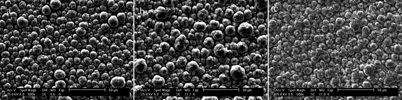
Images (SEM) of electroless Ni–B coatings at 450°C
As seen in Table 1, the surface roughness of the coatings is affected by surface treatment. The surface roughness Ra of 1·22 μm increased to 1·42 μm after the plasma nitriding process. Since sputtering and redeposition occur during the CPN process, the surface roughness of the CPN coating is larger than that of the as deposited one (Fig. 1). An increase in the surface roughness by plasma nitriding was also observed in the literature.26–28 On the other hand, in the ASPN process, sputtering occurs on the screen and only redeposition occurs on the sample surface. Therefore, the surface roughness of these samples is smaller than that of the CPN ones, which was also observed by other researchers.23
Results of surface roughness, microhardness and wear tests of electroless Ni–B coatings under various conditions
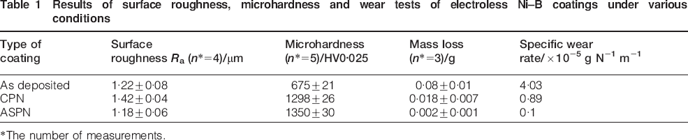
*The number of measurements.
X-ray diffraction pattern
The XRD patterns of the as deposited and treated samples are presented in Fig. 2.
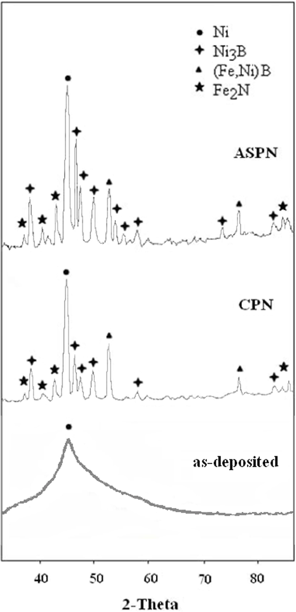
X-ray diffraction patterns of electroless Ni–B coatings
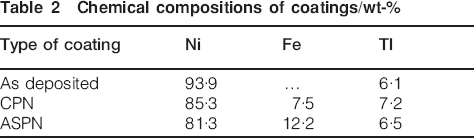
The XRD pattern of as deposited electroless Ni–B coating shows a broad peak at 2θ = 45·16°, which indicates an amorphous structure. Amorphous structure was transformed to crystalline structure by treatments (Fig. 2). As it was shown in pervious studies,1,4–16 crystalline nickel and Ni3B phases were predominant phases in annealed coatings. Neither nickel nitride nor boron nitride is observed in the XRD patterns of nitrided coating. Instead, (Fe,Ni)xB and Fe2N phases are observed beside Ni3B phase. This can be attributed to the sputtering of Fe atoms from steel stage, which was used to hold the samples and was surrounded by plasma during plasma nitriding process. Under the experimental conditions, Fe atoms were sputtered from the stage surface and redeposited on the coating surface. In addition, some of the Fe atoms can combine with nitrogen and redeposit as Fe2N on the coating surface. Sputtering and redeposition of steel active screen in ASPN procedure resulted in more concentration of Fe on the surface of ASPN coating. Therefore, EDS analysis (Table 2) showed more concentration of Fe on the surface of ASPN coating (12·2 wt-) in comparison with the CPN one (7·5 wt-). The EDS analysis only allowed identifying the major components in the coatings. It is not unexpected that boron and nitrogen are not detected by this method as they are light elements.8 Furthermore, good mutual solubility of iron and nickel, which was reported in plasma boriding,17 promotes the formation of (Fe,Ni)xB phase in plasma nitrided coatings.
Chemical compositions of coatings/wt-
Microhardness
The microhardness value of 675 HV0·025 under the as deposited condition increases to a value of 1298HV0·025 with CPN at 450°C, as a post-deposition treatment of the coatings (Table 1). The increase in the microhardness with conventional post-deposition treatment is mainly attributed to the transformation from an amorphous to crystalline structure during precipitation hardening.1–16 The existence of different combinations of Fe with other atoms besides Ni3B phase is the main reason for the superior properties of CPN coating in comparison with the annealed one. Wang29 has also concluded that with the increase in the Fe content in the deposits, the microhardness of deposits increases.
In ASPN coating, even higher microhardness value was obtained compared with the CPN one. This can be resulted from the high concentration of nitrogen in ASPN process. Nagatsuka et al.30 also showed that ASPN procedure can cause more concentration of nitrogen than CPN in samples, which can result in higher microhardness than CPN.
Wear
The wear resistance of the coatings was measured by pin on disc wear test, and the results showed that the mass loss is smaller for treated electroless Ni–B coating. The average mass loss for as deposited, CPN and ASPN coatings were 0·08, 0·018 and 0·002 g respectively. The specific wear rate and mass loss for electroless Ni–B coatings under various conditions are shown in Table 1. These values suggest that the wear rate decreases with increasing microhardness. In case of electroless deposition, harder deposits are always found to wear out slower than the softer deposits.14 Rajendran et al.5 also observed that for a given sort of abrasive particles, the microabrasive wear resistance can be improved by increasing the surface hardness.
The SEM images of worn surface are shown in Fig. 3. The formation of hard phases following the treatments as well as the low mutual solubility between pin and those phases might be responsible for the increase in the wear resistance.11,14,31 Severe removal of as deposited coating occurred during the wear test (Fig. 3a). Since Ni and Co have high solubility in each other, adhesive wear could be considered as a predominant wear mechanism for as deposited coating.22 The smearing of materials (Fig. 3a) and the plate-like debris (Fig. 3d) are all typical characteristics of adhesive wear, which is well established for as deposited electroless coating against many types of materials.11,32 On the other hand, low mutual solubility between pin and Ni3B, (Fe,Ni)xB and Fe2N phases results in abrasive wear.
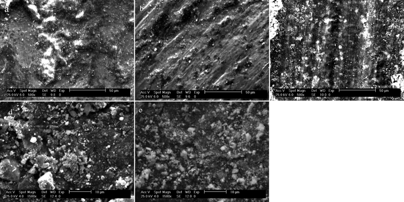
Images (SEM) of wear track and wear debris of a, d as deposited, b, e CPN and c ASPN coatings
The results showed that although the surface roughness of CPN coating is higher than that of the as deposited one, the CPN coating has better wear resistance. It was reported in the literature that a reduction in wear resistance occurs with increasing surface roughness.5 This effect was not observed in CPN coating, since it exhibited higher wear resistance than the as deposited one. This is probably due to an increased resistance to abrasive wear offered by the CPN coating, being more important than the supposed negative effect of the increased surface roughness, which was also concluded by Rajendran et al.5
As can be seen in Fig. 3b and c, the wear track of CPN coating is wider and it has a relatively rougher morphology in comparison with that of the ASPN one. However, the worn surface of ASPN coating (Fig. 3c) shows a smooth conforming surface and new initiation of microcracking. Conclusively, lower surface roughness and higher microhardness can contribute to better wear resistance of ASPN coating than that of the CPN one. Better wear resistance of plasma nitrided coating can result from spherical debris (Fig. 3e), which can roll and result in lesser wear rate than angular debris of as deposited coating (Fig. 3d).31–33 In addition, the fine spherical debris of CPN coating can reside in the wear track and result in a reduction in wear rate as seen in Table 1.22,31 Since in ASPN coating, there was not enough debris to pick up, we were not able to present a photo of its debris.
Conclusions
In the present study, the properties of nitrided electroless Ni–B coatings prepared by CPN and ASPN were investigated. Under the experimental conditions, plasma nitriding of electroless Ni–B coatings resulted in the formation of Ni3B, Fe2N and (Fe,Ni)xB phases, which increases the microhardness of the coatings. It was shown that the wear of untreated coating was severe and characterised by strong adhesion, while the wear of plasma nitrided coating was mild. Active screen plasma nitriding demonstrated less surface roughness and higher microhardness that caused superior wear resistance compared with CPN. These characteristics of ASPN coating can justify its role in surface engineering of industrial components.