
Abstract
Au−30 at-Sn eutectic alloy was fabricated by sequentially pulse electroplating Au and Sn films on Si chips. Three kinds of Au/Sn/Au triple layer films were prepared in the present work: Au/Sn/Au (6/6/1 μm) films, Au/Sn/Au (6/6/6 μm) films and Au/Sn/Au (8/6/1 μm) films. The microstructure and phase transformation in Au/Sn/Au films during aging and reflow soldering were investigated. For Au/Sn/Au (6/6/1 μm) films during aging at 100 and 150°C, the layered AuSn/AuSn2/AuSn4 structure formed in the reaction region. Furthermore, the Sn film was completely consumed, and AuSn4 finally transformed into AuSn and AuSn2 after aging at 150°C for 15 h. For Au/Sn/Au (6/6/6 μm) films during aging at 150°C, the electroplating sequence had an important effect on the formation of Au−Sn phases. An Au5Sn layer was present at the Au II/Sn interface but not at the Au I/Sn interface. For Au/Sn/Au (8/6/1 μm) films, the micropores that formed preferentially along the Au5Sn/AuSn interface remarkably decreased with increasing reflow temperature from 280 to 310°C. After reflowing for 10 s, the microstructure was not an Au−Sn eutectic; however, after reflowing for 60 s, coarsened primary Au5Sn phase and typical Au−30 at-Sn eutectic microstructure of fine eutectic phases (AuSn+Au5Sn) formed.
Introduction
The solder bumps in electronic packaging mainly have three functions: mechanical support, heat dissipation and electrical connection.1,2 Au−30 at-Sn eutectic alloy, a high temperature lead free solder,3 is one of the potential solders for high power light emitting diode chip packaging. The properties of high gold composition and low oxidation in the soldering process, as well as the high thermal conductivity and high strength, make it suitable for fluxless optical assembly applications.4,5
Electroplating of Au−30 at-Sn solder bumps is an attractive alternative, which offers the advantages of low cost and high production as compared to preform6 and evaporation.2,7 Electroplating of Au−30 at-Sn alloys can be carried out by sequentially electroplating8 or by co-depositing.9–11 However, it appears rather difficult to directly deposit Au−30 at-Sn alloys on chips due to the extremely low electroplating rate and the imprecise control of composition. In comparison with the method of co-depositing, the sequentially electroplating of pure Au and Sn films from separate solutions is widely used due to its stable property. In previous work, separate stable non-cyanide electroplating solutions for Au and Sn films were developed.8 The gold solution mainly consisted of sodium gold sulphite [Na3Au(SO3)2], sodium sulphite (Na2SO3) and ethylene diamine tetraacetic acid, which acted as the main salt, the main complexing agent and the second complexing agent for gold respectively. The tin solution mainly contained stannous sulphate (SnSO4), potassium pyrophosphate (K4P2O7.3H2O), ascorbic acid, catechol and nickel chloride (NiCl2). The electroplating parameters were optimised to offer Au and Sn films with high quality and high electroplating rate. Furthermore, Au/Sn/Au triple layer films were successfully fabricated on Si wafer by sequentially pulse electroplating of Au and Sn films.
In general, to prevent the Sn from oxidation, an Au film was deposited on it. The Au−Sn solders can be obtained by alloying the sequentially electroplated triple layer films. Two alloying methods, aging and eutectic reflowing, are commonly applied. It is calculated that, after sufficient alloying process, the Au−30 at-Sn eutectic alloy can be obtained when the initial thickness ratio of Au/Sn films is 3∶2.
Au can form intermetallic compounds (IMCs) with Sn. A thin, continuous and uniform IMC layer is essential to the bonding between the solder and the conductor metal. On the other hand, due to the brittle nature of IMCs, a thick IMC layer at the solder/substrate interface degrades the reliability of solder joints.12,13 Therefore, the formation of interfacial IMCs has a crucial effect on the reliability of Au−Sn solder bumps. The interfacial reactions between Au and Sn in as deposited Au/Sn couples at room temperature were experimentally investigated.14,15 The results showed that the phases in the reaction zone depended on the initial thickness of Sn film and aging time. Furthermore, the Au/Sn/Au triple layer films were reflowed at 320–350°C, and the Au−Sn alloy was denser with fewer internal micropores after reflowing at the higher temperature of 350°C. Yamada et al.16 studied the formation of IMCs in Sn/Au/Sn films during annealing at 160°C, and the kinetics of the reactive diffusion between Au and Sn were experimentally determined. The AuSn4 layer was four times thicker than the AuSn2 and AuSn layers, and the ratio of the IMC layer thicknesses was kept constant during annealing.
In the present work, three kinds of Au/Sn/Au triple layer films were fabricated on Si chips by sequentially electroplating of Au and Sn films. The interfacial reactions in the Au/Sn/Au triple layer films during aging at 100 and 150°C and during reflow soldering were investigated.
Experimental
Separate sulphite gold sodium based solution and stannous sulphate based solution were used to sequentially electroplate Au and Sn films on Si chips (4×9 mm), which were sliced from Si wafers. The Si chips metalised with 0·2 μm Cr and 1 μm Au were used as cathodes. Cr acts as an adhesion and barrier layer, while Au acts as a seed layer for electroplating. The backsides of Si chips were coated with stop-off lacquer to avoid plating. A gold plate of 25 mm diameter was used as anode.
A CS300 electrochemistry test system was used for the power supply of electroplating. A high power magnetic stirrer served for heat preservation and agitation, which kept the electroplating solutions at a constant temperature. Usually, an Au film was first electroplated on Si chips and then followed by a Sn film on top of the Au film in the literatures. In the present work, to prevent the Sn from oxidation, an Au film was adopted on the Sn film. Three kinds of Au/Sn/Au triple layer films were prepared for aging and reflowing: (i) Au/Sn/Au (6/6/1 μm) films were aged at 100°C for 5, 10, 15 and 20 h and aged at 150°C for 5, 10 and 15 h respectively; (ii) Au/Sn/Au (6/6/6 μm) films were aged at 150°C for 5 and 10 h respectively; and (iii) Au/Sn/Au (8/6/1 μm) films were aged at room temperature for two weeks and then reflowed at 280 and 310°C for 10 and 60 s respectively.
The samples were then sealed in epoxy and prepared for microstructural examination. The morphology of the IMCs formed between Au and Sn films was observed using a scanning electron microscope (SEM). The chemical compositions of the Au−Sn phases were identified by energy dispersive X-ray spectrometry (EDX).
Results and discussion
Aging of Au/Sn/Au (6/6/1 μm) films at 100°C
Figure 1 shows the cross-sectional SEM images of the Au/Sn/Au (6/6/1 μm) triple layer films after aging at 100°C for various times. The aging times were 5, 10, 15 and 20 h (Fig. 1a–d). The layered AuSn/AuSn2/AuSn4 structure was observed in the reaction region. It is obvious that the reaction region grew thicker with increasing aging time. In order to identify the layers in the reaction zone, the contents of Au and Sn from the top Au side to the bottom Au side were quantified by EDX. Table 1 lists the compositions of the phases formed between the Au and Sn films after aging at 100°C for various times. AuSn4, AuSn2 and AuSn were identified between the Au and Sn films. AuSn4 was near the top Au film, and AuSn was next to the bottom Au film. Although the AuSn and AuSn2 phases can be discriminated by EDX, there is no difference in SEM images due to the weak contrast between the two layers, as shown in Fig. 1. It is considered that the AuSn and AuSn2 phases cannot be distinguished using SEM; therefore, the two phases were regarded as one layer. Huang et al.17 and Chen and Yen18 reported the similar AuSn/AuSn2/AuSn4 structure in the reaction regions of Au/Sn films after aging at 150°C and Sn−Ag/Au couples after aging at 200°C respectively, which is consistent with the present research result.
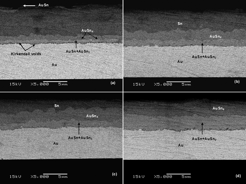
Cross-sectional SEM images of Au/Sn/Au (6/6/1 μm) films after aging at 100°C for various times (×5000)
1 Compositions of phases formed in Au/Sn/Au (6/6/1 μm) triple layer films (from top to bottom in Fig. 1) after aging at 100°C for various times
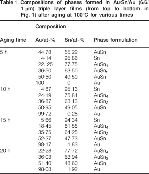
Figure 2 shows the thicknesses of the reaction layers in the Au/Sn/Au (6/6/1 μm) films during aging at 100°C. It is obvious that the consuming rate of Sn was much faster than that of Au. There was still ∼4·5 μm Au remaining on the Si chip after aging for 20 h, but all the Sn had been consumed. It is noted that, when the aging time was <15 h, the AuSn4 and (AuSn+AuSn2) layers approximately grew as parallel lines, indicating that they had similar growth rates. When the aging time was >15 h, the growth rate of the (AuSn+AuSn2) layer exceeded that of the AuSn4 layer. Figure 2 shows that the reaction layers (AuSn/AuSn2/AuSn4) were much thicker when the aging time was >15 h. Thus, the diffusion of Au atoms across the reaction layers into Sn film was retarded, and then the formation of AuSn4 phase was slowed down. On the contrary, the AuSn4 phase gradually transformed into (AuSn+AuSn2) phases with increasing aging time. As a result, the growth rate of the (AuSn+AuSn2) layer exceeded that of the AuSn4 layer. When the aging time increased to 20 h, the Sn was almost completely consumed. This implies that the AuSn4 layer would finally transform into AuSn2 and AuSn with increasing aging time. The imbalance diffusions of Au and Sn atoms, i.e. the diffusivity of Au atoms is much faster than that of Sn atoms, resulted in Kirkendall voids at the interface of the bottom Au film.
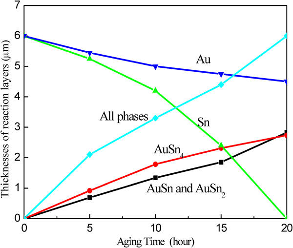
Thicknesses of reaction layers in Au/Sn/Au (6/6/1 μm) films versus aging time at 100°C Aging of Au/Sn/Au (6/6m/1 μm) films at 150°C
Figure 3 shows the cross-sectional SEM images of the Au/Sn/Au (6/6/1 μm) triple layer films after aging at 150°C for various times. The aging times were 5, 10 and 15 h respectively. It is obvious that the layered structure in the reaction region was obviously different from that during aging at 100°C. The entire Sn film disappeared after aging for 5 h, and the AuSn4 phase completely transformed into the AuSn and AuSn2 phases after aging for 15 h. It is clear that the higher the aging temperature was, the faster the growth rates of Au−Sn layers became. Therefore, the transformation from AuSn4 phase into AuSn and AuSn2 phases at 150°C was faster than that at 100°C. According to the initial thicknesses of Au and Sn films, it is inferred that the AuSn4 and AuSn2 phases would finally transform into the AuSn phase, no matter aging at 100 or 150°C.
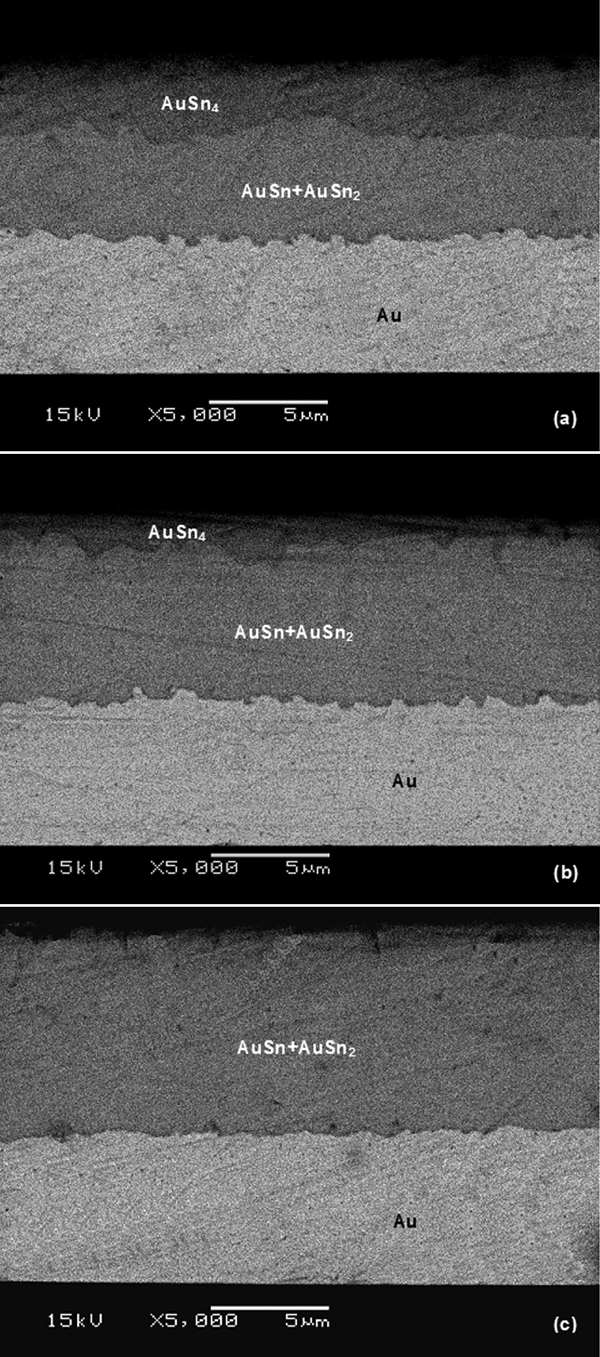
Cross-sectional SEM images of Au/Sn/Au (6/6/1 μm) films after aging at 150°C for various times (×5000)
Aging of Au/Sn/Au (6/6/6 μm) films at 100°C
The Au/Sn/Au (6/6/6 μm) triple layer film on Si chips was designed to study the effect of electroplating sequence on the interfacial reaction during aging. The Au film near the Si chip was marked with Au Ι, and the other was marked with Au II. Figure 4 shows the cross-sectional SEM images of the Au/Sn/Au (6/6/6 μm) films after aging at 150°C for 5 and 10 h respectively. It is shown that there was an unexpected layer at the Au II/Sn interface that was not present at the Au Ι/Sn interface. Energy dispersive X-ray spectrometry identified that the composition of this layer was 85·2 and 50·7 at-Au from top to bottom, corresponding to Au5Sn and AuSn phases. The formation of an Au rich phase (Au5Sn) at the Au II side indicated that the Sn was the dominant diffusion element. However, the diffusivity of Sn in Au is about 13–15 orders of magnitude less than that of Au in Sn at room temperature.19 Thus, there was a discrepancy in the diffusivity of Au and Sn.
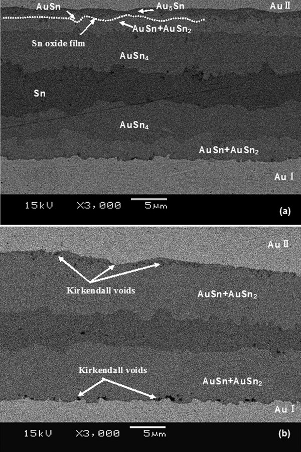
Cross-sectional SEM images of Au/Sn/Au (6/6/6 μm) films after aging at 150°C for various times (×3000)
In order to identify the reason why the Au5Sn phase formed at the Au II/Sn interface, more research work was carried out. It is well known that oxidation on the surface of Sn occurs if Sn is exposed to air or water containing dissolved oxygen. In the present experiment, the Sn layer was exposed in air before the electroplating of the Au II layer. Furthermore, a small amount of oxygen element was identified by EDX on the surface of the Sn film in the reaction region. Therefore, a thin Sn oxide was present on the surface of Sn film; however, what kind of Sn oxide in the present work cannot be determined. Tang et al.14 reported a similar phenomenon at room temperature, and they found that a 1·5 nm SnO2 film in the Sn/Au couple formed during cleaning the electroplated Sn film with deionised water before immersing in the Au plating solution. It is deduced that the Sn oxide significantly retarded the diffusion of Au atoms from the Au side into the Sn side. Figure 5 shows the top view SEM images of the electroplated Au and Sn films. The grain size of the Au film was much smaller than that of the Sn film, indicating that there were more grain boundaries in the Au film per unit area. Therefore, Sn atoms could diffuse into the Au film via grain boundary diffusion after they passed through the thin Sn oxide. It is considered that the above factors contributed to the formation of Au5Sn. At the beginning of the reaction, Sn atoms diffused across the Sn oxide and reacted with Au atoms to form Au5Sn

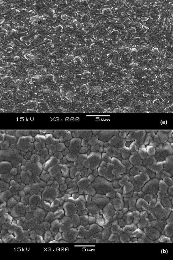
Top view SEM images of as electroplated films (×3000)
Here, the symbol [Sn] denotes the diffusing Sn atoms in the Au film, and it does not represent pure Sn.
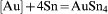
Simultaneously, the Au5Sn would continuously react with Sn atoms to form the AuSn phase

At the same time, Au atoms diffused across the Sn oxide into the Sn film to form Sn rich AuSn4 phase
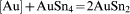
Here, the symbol [Au] denotes the diffusing Au atoms in the Sn film; it does not represent pure Au. Then, the Au atoms reacted with AuSn4, leading to the nucleation of AuSn phase at the Au/AuSn4 interface

As the AuSn layer grew, the amount of Au atoms that arrived at the AuSn4/AuSn interface decreased. The product was changed, and the AuSn2 phase formed at the AuSn4/AuSn interface
The IMCs formed between the Au and Sn films grew with increasing aging time; therefore, Sn atoms could hardly diffuse through the IMC layers. Thus, reaction (2) was significantly retarded. When the aging time was <5 h, Au5Sn layer still remained near the Au II side. When the aging time increased to 10 h, the Sn and Au5Sn layers disappeared, while the (AuSn+AuSn2) and AuSn4 layers were present at the interface.
As shown in Fig. 4b, Kirkendall voids were observed at both Au Ι and Au II interfaces. Furthermore, the size of Kirkendall voids at the Au II interface was much smaller than that at the Au Ι interface, confirming the fact that the diffusion of Au atoms from the Au II side into the Sn side was significantly retarded. It is concluded that the electroplating sequence had an important effect on the formation of IMCs between the Au and Sn films.
Reflowing of Au/Sn/Au (8/6/1 μm) films
The Au/Sn/Au (8/6/1 μm) triple layer film on Si chips was aged at room temperature for 2 weeks and then reflowed to obtain Au−30 at-Sn eutectic solders. Figure 6 shows the cross-sectional SEM images of the Au/Sn/Au (8/6/1 μm) films after reflowing at 280 and 310°C respectively.
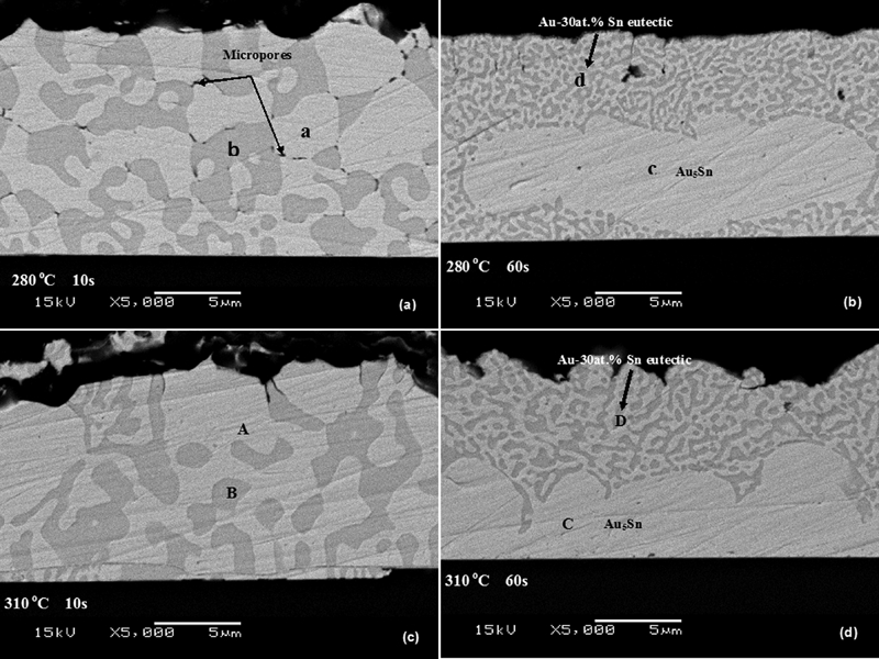
Cross-sectional SEM images of Au/Sn/Au films (8/6/1 μm) after reflowing (×5000)
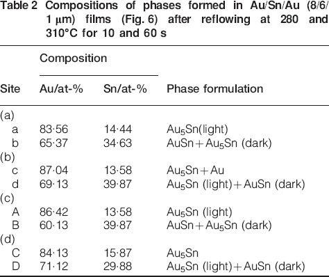
Figure 6a and c shows the microstructure of Au−Sn alloys after reflowing at 280 and 310°C for 10 s respectively. Table 2 lists the compositions of the phases formed between the Au and Sn films at certain areas. The phases in the a and A areas contained 83·56 and 86·42 at-Au respectively, which were identified to be Au5Sn. The phases in the b and B areas contained 65·37 and 60·01 at-Au, which were identified to be a mixture of AuSn and Au5Sn, but not the Au−Sn eutectic. During reflowing, the electroplated Sn film melted first at ∼232°C, accelerating the reaction between the molten Sn with the Au–Sn intermetallics, the electroplated Au film and the Au seed layer on Si substrate. When the temperature increased to 280°C or higher, a liquid alloy with a uniform Au and Sn composition formed. During cooling to room temperature, the liquid alloy will solidify via the eutectic reaction and form the mixture of fine AuSn and Au5Sn phases. In the present work, since there was an Au seed layer on the Si chip, the Au content was higher than the eutectic value of 70 at-Au; therefore, a hypoeutectic Au−Sn alloy was obtained. The Au rich phase (Au5Sn) first precipitated from the liquid phase during solidification. When the temperature decreased to the eutectic point, the eutectic would form. However, there was not enough time for the alloying of Au and Sn atoms to form a uniform liquid alloy due to such a short reflow time. Furthermore, the IMCs formed during aging at room temperature also need time to be molten in the Au−Sn liquid. Therefore, the microstructure formed after reflowing for 10 s was not the Au−Sn eutectic.
2 Compositions of phases formed in Au/Sn/Au (8/6/1 μm) films (Fig. 6) after reflowing at 280 and 310°C for 10 and 60 s
It is obvious that when the Au/Sn/Au (8/6/1 μm) triple layer film was reflowed at 280°C (Fig. 6a), some micropores formed preferentially along the grain boundaries. When the reflow temperature increased to 310°C, the number of micropores in the Au−Sn alloy decreased (Fig. 6c). The micropores might be caused by volume shrinkage during solidification. It is considered that the higher reflow temperature decreased the viscosity and surface tension of the liquid Au−Sn alloy, resulting in the decrease in the number of micropores.
Figure 6b and d shows the Au/Sn/Au (8/6/1 μm) triple layer films after reflowing at 280 and 310°C for 60 s respectively. The phases in the c and C areas contained 87·01 and 84·13 at-Au, which were identified to be Au5Sn. While the microstructure in the d and D areas contained nearly 70 at-Au, which were identified to be the typical Au−Sn eutectic microstructure, with an alternating distribution of the two fine eutectic phases AuSn and Au5Sn. When the reflow time increased to 60 s, a liquid Au−Sn alloy with a uniform Au and Sn composition formed. The Au5Sn phase first precipitated from the liquid phase, and then the eutectic transformation occurred during solidification. As a result, the microstructure of coarsened primary phase Au5Sn and fine eutectic phases (AuSn+Au5Sn) was observed. Therefore, a higher reflow temperature of 310°C and a longer reflow time of 60 s were the benefits of the formation of the Au−Sn eutectic structure.
Conclusions
The layered AuSn/AuSn2/AuSn4 structure was observed in the reaction region of the Au/Sn/Au (6/6/1 μm) film during aging at 100 and 150°C. During aging at 100°C, the AuSn4 and (AuSn+AuSn2) layers had similar growth rates at the initial stage, and the growth rate of the (AuSn+AuSn2) layer exceeded that of the AuSn4 layer when the aging time was >15 h, since the diffusion of Au atoms was blocked by thick reaction layers (AuSn/AuSn2/AuSn4). After aging at 150°C for 15 h, the Sn film was completely consumed, and the AuSn4 finally transformed into AuSn and AuSn2.
The electroplating sequence had an important effect on the formation of Au−Sn phases in the Au/Sn/Au (6/6/6 μm) film during aging at 150°C. An Au5Sn layer was present at the Au II/Sn interface but not at the Au Ι/Sn interface. A thin Sn oxide that formed on top of the Sn film during the electroplating process significantly retarded the diffusion of Au atoms into the Sn side, and the Sn atoms could diffuse rapidly in Au due to a higher density of grain boundary in the electroplated Au film, resulting in the formation of Au5Sn phase at the Au II/Sn interface.
The Au/Sn/Au (8/6/1 μm) films were aged at room temperature for 100 h and then reflowed at 280 and 310°C for 10 and 60 s respectively. The micropores that formed preferentially along the Au5Sn/AuSn interface remarkably decreased with increasing reflow temperature from 280 to 310°C. After reflowing for 10 s, the microstructure was not an Au−Sn eutectic due to insufficient reflow time. However, after reflowing for 60 s, coarsened primaryAu5Sn phase and typical Au−30at-Sn eutectic microstructure of fine eutectic phases (AuSn+Au5Sn) formed due to the hypoeutectic transformation. It is indicated that a higher reflow temperature of 310°C and a longer reflow time of 60 s were the benefits to the formation of Au−Sn eutectic microstructure.
Footnotes
Acknowledgements
The present work was supported by the programmes of the National Natural Science Foundation of China (grant no. U0734006 and no. 51171036), the programmes in Liaoning Province (grant no. 2009921058 and no. 20082163) and the Key programme in Dalian (grant no. 2006A11GX005).