
Abstract
The aim of the present investigation is to understand the localised failure mechanism of diamond-like carbon (DLC) film during multiple load cycle nanoindentation. The DLC film investigated was 500 nm thick sputter coated on Si (100) wafer of 500 μm thickness. Multiple load cycle nanoindentation tests under diamond Berkovich and conical indenters were performed using a calibrated NanoTest at five different load ranges between 0·1 and 500 mN. Test results indicated forward deviation, no deviation and backward deviation of the force–displacement profile, which provided some insights to the mechanisms of localised film failure. During backward deviation, film failure starts from interfacial delamination. This was observed for a conical indenter in a particular load range (1–10 mN). An elastic finite element model during nanoindentation loading indicated that this was caused by the location of maximum stress near the interface. Forward depth deviation was observed for conical and Berkovich indenter at all the other load ranges.
Keywords
List of symbols
acoustic emission
atomic force microscope
backward depth deviation
diamond-like carbon
elastic modulus
elastic modulus of indenter
reduced elastic modulus
elastic modulus of substrate (specimen)
forward depth deviation
finite element method
focused ion beam
depth (displacement)
hardness
contact depth (displacement)
equal depth (displacement)
final depth (displacement)
maximum depth (displacement)
intensity ratio of D and G banks
microelectromechanical systems
nanoelectromechanical systems
nanocrystalline diamond
optical microscope
force
final (residual) force
loading force
unloading force
physical vapour deposition
radio frequency
radius of curvature (before)
radius of curvature (after)
standard cubic centimetre per minute
thickness of the Si substrate
thickness of DLC film
Poisson's ratio (substrate or indenter)
residual stress, compressive residual stress
Introduction
Although hardness (H) is a commonly reported measurement, it is not always the most relevant property in the design process. In recent times, there has been a considerable improvement in instrumented indentation experimental systems, and it is now possible to monitor both the force (P) and the displacement or depth (h) during the indentation cycle in materials at macro-/micro-/nanoscales.1,2 The present paper considers the specific case of diamond-like carbon (DLC) thin film behaviour during multiple load cycle nanoindentation via force–displacement (P–h) profile and subsequent imaging of indentation by atomic force microscope (AFM) and focused ion beam (FIB) imaging.
The DLC thin films are currently used in solar panels, biomedical implants, microelectromechanical systems/nanoelectromechanical systems, cutting tools and a range of other applications. Understanding the nanomechanical behaviour of DLC thin films is critical for optimising film design for improved durability and performance.2,3 Single load cycle nanoindentation has been employed for evaluating the deformation and cracking behaviour of DLC films coated on silicon substrate in a number of recent investigations.4,5 This technique can be extended to multiple load cycle nanoindentation tests, which offer a capability to evaluate the fracture behaviour 6 for nanoscale tribological phenomenon and also contact fatigue of components. These nanomechanical investigations can also lead to improved understanding of nano-/microscale asperity interactions in manufacturing processes. 7
Deformation or cracking can appear in thin films during residual stress (pre-existing) relaxation and due to in service loading due to asperity interactions, impact and low or high cycle fatigue. To obtain a more detailed understanding of film failure, knowledge of the instrumented indentation P–h profile characteristics is essential.1–5,8–13 Film failure under different indenter shapes and pre-existing residual stress are interrelated properties. 14 In order to improve the durability of existing thin film coated components, it is becoming increasingly important to take advantage of the advancements in instrumented indentation systems to understand the failure mechanisms in thin films using different indenter shapes at both lower strain rates (e.g. nanoindentation1–6,8–10) and higher strain rates (e.g. nanoimpact14–16). Over the past decade, a number of investigations have considered nanoscale multiple cycle nanoindentation for a number of industrial applications.3,6,15 These investigations take advantage of the typical features in the P–h profile 8 recorded during repeated loading–holding–unloading segments of the test profile in bulk materials and thin films.
Raju et al. 17 investigated the role of pre-existing compressive residual stress in thin films (TiN and AlN) during repeated nanoindentation at the same maximum load. However, since then, very little work has been published dealing with indentation based residual stress relaxation leading to film failure. Authors have recently investigated a nanoimpact based method of characterising the low cycle impact fatigue and multiple load cycle nanoindentation behaviour in 100 nm thick DLC film14,18,19 with a view to quantitatively and qualitatively evaluate the key features of film failure. The present investigations are aimed at investigating the failure of a relatively thick (500 nm) DLC film and understand material accommodation behaviour during multiple load cycle nanoindentation using Berkovich and conical indenters.
Experimental
Test specimen
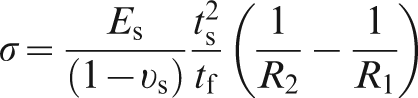
A DLC film of 500 nm thickness was deposited on a 4 in. Si (100) wafer of 500 μm thickness using sputtering of graphite target in pure Ar atmosphere without intentional substrate heating. The base pressure of the deposition chamber was 2×10⁻⁶ torr. The substrate holder was rotated during deposition for film uniformity. The substrate to target distance was 100 mm. The argon gas flowrate was 15 sccm, and the pressure was 5 mtorr. The radio frequency plasma power was 150 W, and the deposition rate was 12·5 nm min−1. The deposition duration was adjusted to achieve a film thickness of 500 nm. Raman spectra were recorded using a spectrometer (Renishaw Raman System 3000). The line at 514·5 nm of a He–Ne laser was used as the exciting source. The wafer curvature before and after film deposition was measured using a profilometer, and the pre-existing residual stress σ was calculated from the changes of radius of wafer curvature (R1 and R2) of the bilayer structure using Stoney's equation (1)
20
Nanoindentation testing and measurements
Nanoindentation measurements (e.g. hardness and elastic modulus) were performed using a calibrated NanoTest system (Micro Materials Ltd, UK) with a standard diamond Berkovich indenter. The nanoindentation testing instrument is a pendulum based depth sensing system, with the specimen mounted vertically and the load applied electromagnetically. A current in the coil causes the pendulum to rotate on a low friction pivot so that the diamond probe penetrates the film surface. Test probe displacement is measured with a parallel plate capacitor. Further detail of the testing instrument and measurement can be seen elsewhere. 21 The P–h profiles were analysed using standard methods with the area function for the Berkovich indenter, which was determined by indentations into fused silica with elastic modulus of 69·9 GPa. Raw data (P–h profile) were used to evaluate the hardness (H) and reduced elastic modulus (Er) using the method of Oliver and Pharr. 8 The elastic modulus (Ei) and Poisson's ratio (νi) of the diamond indenter were taken as 1140 GPa and 0·07, whereas to calculate the elastic modulus (Es) of the specimen (DLC thin film), the Poisson ratio for the DLC thin film (νs) was taken 22 as 0·22.
The hardness and elastic modulus evaluation of thin films requires very careful assessment of test parameters as the measured property may represent a combination of film/substrate properties instead of film. A number of investigations have indicated this dependence.23–25 Although a general rule of penetration depth one-tenth of the film thickness has been recommended by Haanappel et al. 23 , the one-twentieth rule has also been suggested. 24 Chudoba et al. 25 have indicated that these rules are often not practicable for film thickness values below 1 μm. In order to investigate this dependence in the present investigation, the nanoindentation test loads of 1 mN and 100 μN were chosen, which corresponded to a penetration depth of one-eighth and one-twenty-fifth of the film thickness respectively. The indentation instrument also consisted of an optical microscope and an integrated AFM, directly linked by an automated positioning system.
Multiple load cycle nanoindentation testing and measurements
The multiple load cycle nanoindentation with increasing load (also called as multicycle load controlled ‘load–partial–unload’ 26 ) was performed using the above mentioned NanoTest instrument. The indentation procedure was programmed as three segments of trapezoidal shape. The first segment increased the load to a maximum value of 10 s, following a 5 s holding segment at the maximum load. The third segment retrieved the indenter tip from the sample in 10 s to 30 of the test load before reloading for next cycle. The load was increased 100 of the value of the initial load for every indentation cycle. Other experimental conditions during testing were preset initial load 0·3 μN (at zero depth) and 60 s holding period at 90 final unload for thermal drift correction. The load values ranged from 0·1 to 500 mN (Table 1). Each test was conducted for a total of 10 incremental multiple load cycles for both indenter shapes (Berkovich and conical). The Berkovich indenter used had an included angle of 142·3° with a centreline to face angle of 65·3°, whereas the conical indenter had a 10 μm tip radius with 60° cone angle (also termed as blunt spherical tip). Post-indentation testing, the residual impression was characterised using in situ AFM (Nanosurf Nanite, SPM S50, Switzerland). The AFM images were recorded by scanning the specimen surface with a scan rate of 1 Hz. Image processing and data analysis software (Nanite B, v2·2·0) was used for image analysis. Nanoindentation tests and AFM measurements were taken at the instrument chamber temperature, which was set at 23°C. The instrument chamber was an enclosure with temperature controlled environment and an antivibration table to eliminate the influence of temperature, vibrations and noise. In order to minimise the effect of instrument thermal drift, a period of thermal stabilisation was achieved before each test. Post-indentation testing, some of the indentation residual impression was characterised using FIB milling and imaging (JEM-9320FIB, JEOL Ltd, Japan) in order to investigate cracking in the film–substrate system.
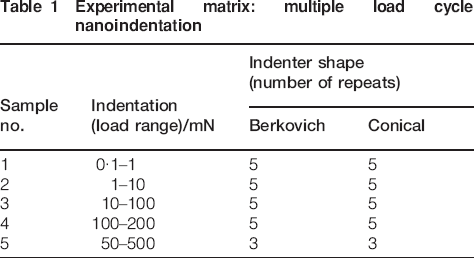
Experimental matrix: multiple load cycle nanoindentation
Results
DLC film characterisation
Raman spectra analysis of the 500 nm thick DLC film showed the typical G bank peak at 1522·3 cm−1 and D band peak at 1326·2 cm−1, and the ID/IG ratio of ∼0·65. Further details about the Raman spectra can be appreciated elsewhere. 27 The measured values of DLC thin film hardness (H) and elastic modulus (E) from single cycle Berkovich nanoindentation test results at 100 μN load were 19±1 and 196±17 GPa respectively and at 1 mN load were 18±1 and 189±4 GPa respectively. These average values at two different penetration depths were very similar, indicating that the influence of substrate and indentation size effect was minimal at these loads. The elastic modulus values can be influenced by the Poison's ratio (νs) of the film. Cho et al. 22 recommended a Poison's ratio value between 0·22 and 0·39, whereas Couvy et al. 13 have indicated a lower value of 0·07. From the present investigation, a sensitivity analysis indicates that the average modulus will change by 4·6 and 10·7 if a lower value of 0·07 or a higher value of 0·39 is used respectively. The measured average value of pre-existing residual stress from the curvature method (equation (1)) was 1·471±0·99 GPa (compressive). This is in lower range of the residual stress values in DLC films as reported by Holmberg et al., 28 where compressive residual stress values in published literature for physical vapour deposited DLC films range from 0·5 to 12·5 GPa.
Multiple load cycle nanoindentation (Berkovich indenter)
Figure 1a shows the typical P–h profiles of multiple load cycle Berkovich nanoindentation obtained for DLC film at 0·1–1·0 and 100–200 mN loads, whereas Fig. 1b shows distinct features in the P–h profile (magnified view of some of the indentation cycles that correspond to Fig. 1a). Figure 1c and d shows the corresponding residual AFM images and topography after the final cycle of indentation. As shown in Fig. 1b(i), it should be noted that each loading curve (OA) and each holding curve (AB) are forward progressing during each indentation cycle, and each unloading curve (BC) is backward progressing. This type of nanoindentation cycle profile is defined here as forward depth deviation (FD). In this case, using the ‘equal displacement approach’, 1 the loading force is greater than the unloading force (i.e. PL>PU). The P–h profile using the Berkovich indenter indicated only forward depth deviation (FD) for all repeats and at all load ranges considered in the present investigation.
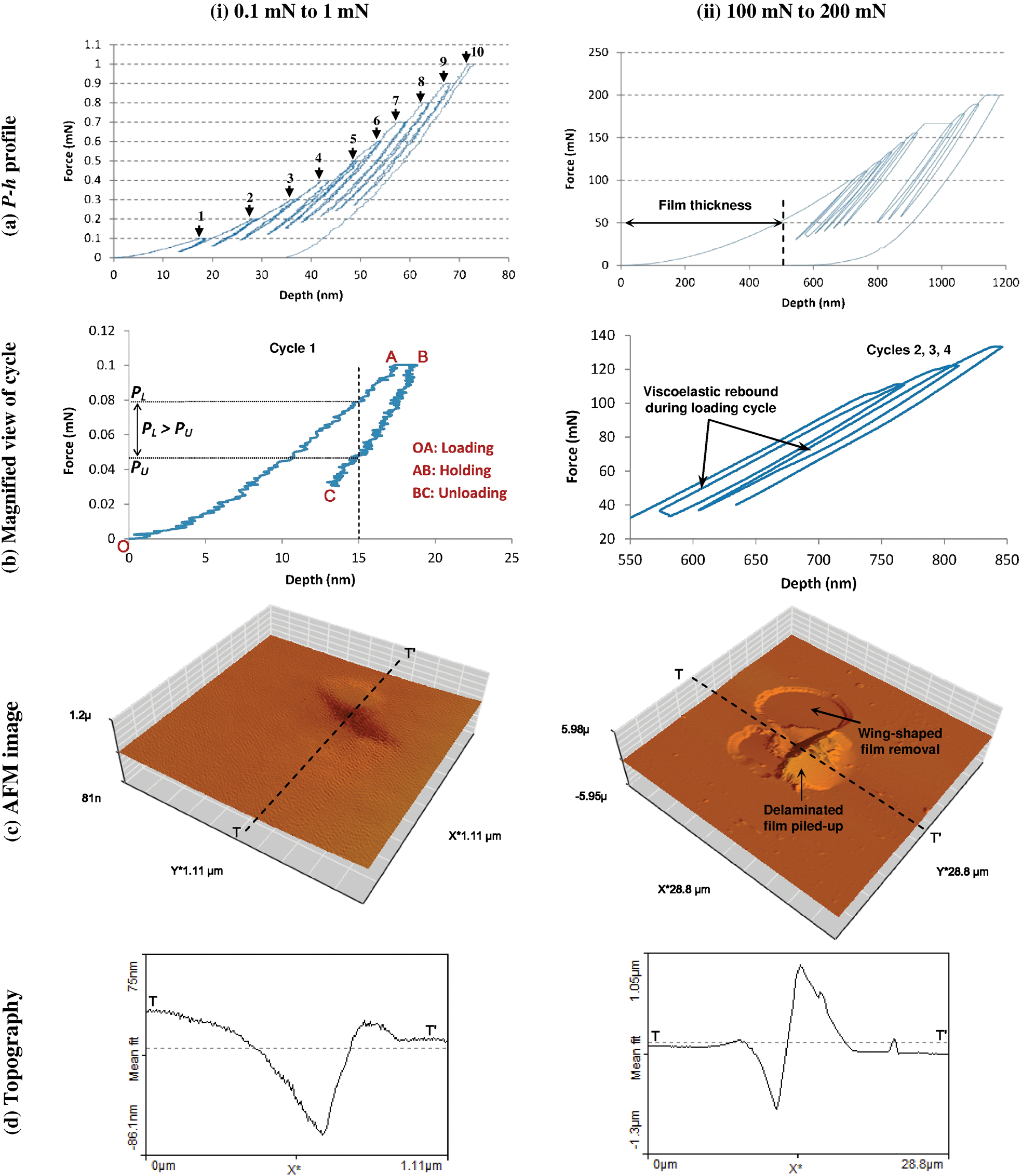
a record of force-depth measurement; b corresponding magnified view of indentation cycle; c corresponding AFM image after final cycle; d corresponding topography passing through centre of residual impression indicated with dotted TT’ line in b indicating pile-up and removal of thin film from substrate
Nanoindentation experiments using the Berkovich indenter indicated that DLC film fracture (both cohesive and adhesive, including typical wing shaped film delamination around the indentation edge) can occur for loads between 100 and 200 mN [e.g. Fig. 1(ii)], observed for each of the five repeats. In Fig. 1b(ii), a small viscoelastic rebound can be observed in the P–h profile, which causes hysteresis loops to appear in the loading and unloading profiles, observed for each repeat at the studied load range (less dominant in some of the cycles for 1–10 and 10–100 mN, much dominant in each cycle for 100–200 mN). It is to be noted that significant indenter penetration has occurred immediately with the onset of indentation [i.e. cycle 1, well beyond the film thickness of 500 nm, Fig. 1a(ii)] using the Berkovich indenter, which is indicative of significant film and substrate failure. At the lowest load range (0·1–1·0 mN), the indentation measurement mainly include thin film but at higher load range (Table 1), and the measured property represents a combination of film/substrate properties.
Multiple load cycle nanoindentation (conical indenter)
Figure 2 presents three types of P–h profiles of multiple load cycle conical nanoindentation for the DLC film at 1–10 and 10–100 mN loads. As shown (for type I) in Fig. 2a(i) and b(i), each loading curve is forward progressing during each indentation cycle, each holding curve is forward progressing during each indentation cycle and each unloading curve is backward progressing. Similarly (for type II) in Fig. 2a(ii), at higher unloading force (i.e. push-up) using the ‘equal displacement approach’, it should be noted that each loading curve is forward progressing during each indentation cycle, each holding curve is backward progressing during each indentation cycle and each unloading curve is backward progressing. Also shown (for type III) in Fig. 2b(ii) is a cycle (cycle 1) where the unloading curve follows back the same path of loading curve and shows neither forward nor backward depth deviation during the holding period (an indication of an ideally elastic response, i.e. PL = PU).
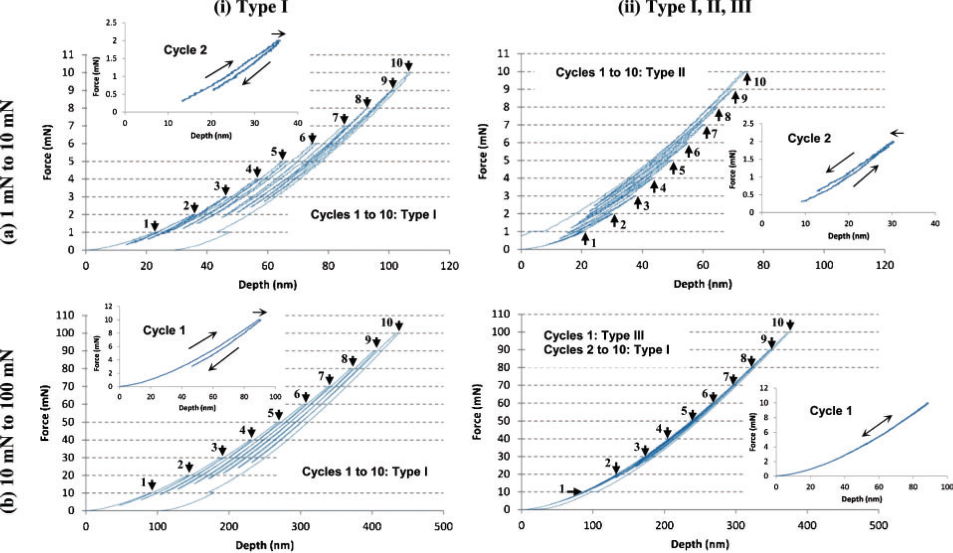
a 1–10 mN; b 10–100 mN
Considering the P–h profile [type II, Fig. 2a(ii)], there is also resistance (induced) to the indenter penetration in the consecutive loading cycle. This type of indentation cycle profile is defined here as backward depth deviation (BD). In this case, using the ‘equal displacement approach’, the loading force is less than the unloading force (i.e. PL<PU).
Table 2 summarises the types of P–h profiles under the conical indenter, indicating the combination of forward and backward depth deviations. For a lower load range (e.g. 1–10 mN), the P–h profiles show backward depth deviation, whereas for the lowest load range (0·1–1·0 mN) and medium to higher load range (10–100, 100–200 and 50–500 mN), only forward depth deviation can be observed for all repeats.
Summary of P–h profile characteristics (conical indenter)
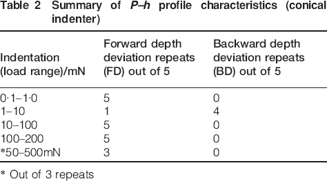
* Out of 3 repeats
Figure 3a and b shows the AFM images and topography for load range at 1–10 mN [which corresponds to Fig. 2a(i) and (ii) respectively] after the final indentation cycle. Figure 3a indicates a forward depth deviation feature, whereas Fig. 3b indicates a backward depth deviation feature. In other results, the degradation of the DLC film mainly included deformation and pile-up around indentation edge with no observable surface cracking for load range as high as 100–200 mN. This behaviour was observed for each of the five repeats. Similar to the Berkovich indenter, a small viscoelastic rebound in P–h profile was observed under the conical indenter, which causes hysteresis loops to appear in the loading and unloading profiles, as observed for each repeat at the studied load range (less dominant in some of the cycles for 10–100 and 100–200 mN).
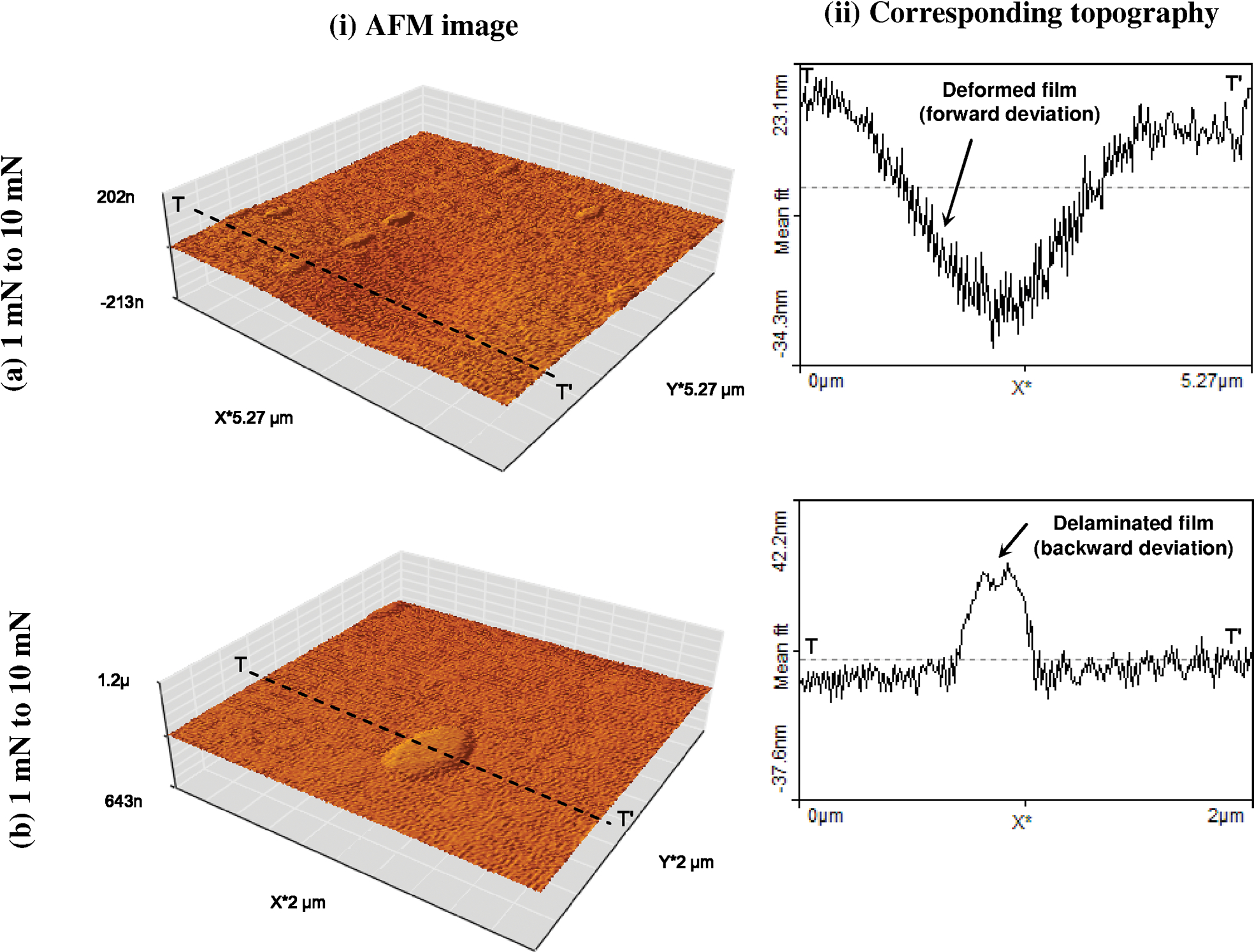
a forward depth deviation; b backward depth deviation
High load multiple load cycle nanoindentation (Berkovich and conical indenters)
Figure 4 shows the results for high load range of 50–500 mN to investigate the types of catastrophic DLC film failure during multiple load cycle nanoindentation using Berkovich and conical indenters, as shown in Fig. 4a(i) and b(i); both examples indicated P–h profiles of type I.
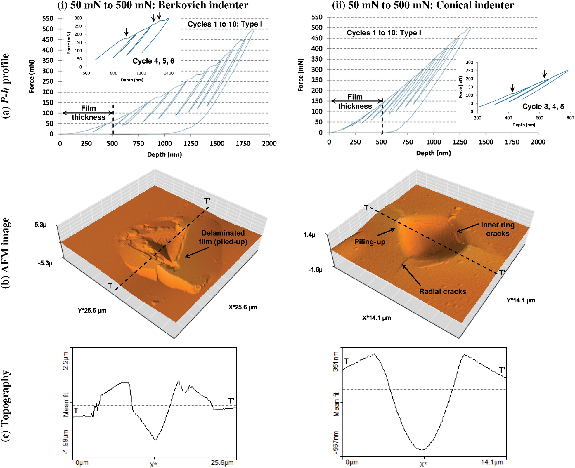
a full record of force-depth measurement indicating forward depth deviation: zoomed in view shown in inbox for some indentation cycles indicating pop-ins (downward arrows) during last stage of some loading cycles; b corresponding AFM image; c corresponding topography passing through centre of residual impression indicated with dotted TT’ line indicating pile-up and removal of thin film from substrate
It should be noted that significant indenter penetration has occurred immediately with the onset of indentation (higher for Berkovich), which is indicative of significant degradation of the film and substrate. A small viscoelastic rebound can also be observed, which causes hysteresis loops to appear in the loading and unloading profile (dominant in later cycles). As shown in the corresponding AFM images and topography (Fig. 4b and c), it should be noted that the Berkovich indenter penetrated well into the substrate and induced significant cracking and delamination in the film–substrate system, whereas the conical indenter induced inner ring cracks within the contact zone and radial cracks in four directions with significant pile-up (an indication of film delamination) around the indentation and ‘pinned’ at the centre of indentation. The occurrence of a ‘pop-in’ observed (higher for Berkovich indenter) during the last stage of each loading cycle (Fig. 4a) is an indication of significant film and substrate cracking during the later stages of loading cycles.
Discussion
Multiple cycle nanoindentation residual impression
To analyse the DLC thin film and substrate degradation (deformation or cracking) during multiple cycle nanoindentation testing, residual impressions were observed using AFM and FIB imaging after the final indentation cycle. As shown in the results section, the thin film failures under the indenters were dominated by cracking, delamination, deformation and relaxation of the pre-existing residual stress.4,5 The Berkovich indenter used is expected to initiate cracking failure at the zone of high tensile (normal) stress concentration,1,2 leading to interfacial film delamination, as indicated in Figs. 1c(ii), 4b(i) and 5a. Under the Berkovich indenter when the penetration depth is greater than the film thickness, the indenter penetrates more into the substrate in each load cycle due to plastic deformation and cracking of the Si substrate.4,5 This can be seen in the FIB image shown in Fig. 5a for load range of 100–200 mN, which indicates significant delamination of thin film from the substrate with no radial cracking but some indentation edge cracking within the substrate. For the case of the conical indenter, the observations indicate debonding of the DLC film at the film/substrate interface [Figs. 3b(ii), 4b(ii) and 5b]. No brittle cracking in the thin film was observed in the surface observations for load range as high as 100–200 mN for any of the repeats for conical indenter. However, as shown in the FIB image in Fig. 5b for load range of 50–500 mN, significant brittle cracking of thin film in the form of through thickness ring cracks from the substrate and relaxation of thin film in the form of curling-up and lateral meshed cracking within substrate 5 was observed. There can be some reduction in the thickness of the thin film in the region below the indenter, indicating plastic deformation of the thin film;4,5 however, in the present investigation (Fig. 5b), this local compression was not observed using FIB imaging.
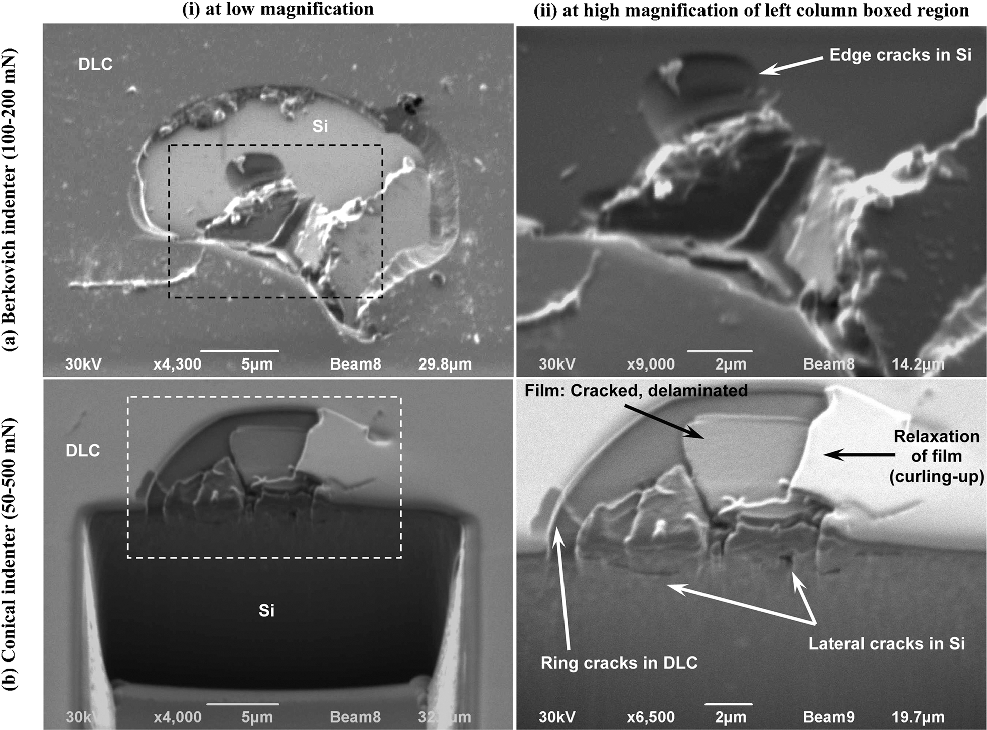
a surface image for 100–200 mN load range (Berkovich indenter) indicating delamination of thin film from substrate, no radial but edge cracking within substrate; b cross-section image passing through centre of indentation for 50–500 mN (conical indenter) load range indicating removal of thin film in form of ring cracks from substrate, relaxation of thin film in form of curling-up and lateral meshed cracking within substrate
The interfacial delamination failure showed a distinct feature indicating backward depth deviation at a lower load range (1–10 mN, repetitions shown in Table 2) using the conical indenter. This behaviour of backward depth deviation has been previously investigated by Faisal et al. 14 in nanoimpact (1000 impacts at 1 mN load using NanoTest system) testing of 100 nm thick DLC film. It has been indicated that film delamination at the interface is possible without surface cracking and significant reduction in contact depth (i.e. backward depth deviation). The depth deviation has been further investigated by Ahmed et al. 18 during nanofatigue test using the TriboIndenter system (Triboscope, Hysitron Inc., Minneapolis, MN, USA) equipped with Berkovich indenter, where 100 nm thick DLC film failure starts as cohesive failure via cracks perpendicular to the film/substrate interface, which is followed by film decohesion from the interface. This behaviour of backward depth deviation leading to film delamination (in the form of blisters) has also been previously investigated under single cycle indentation.29–31 It has been described that the elastic energy in the film available to drive the interface delamination arises from pre-existing residual stress (compressive) in the film and additional stress induced in the film during indentation.1,2,29,30 The film–substrate system is forced by the indenter to displace radially in its own plane, and the strain mismatch between film and substrate leads to out of plane bending in the film due to the vertical deflection of the substrate induced by the indenter. 29 Hence, this behaviour of backward depth deviation of the relatively thick (500 nm) film in the present investigation was consistent with previous findings on 100 nm thick coatings, with the exception that in the present investigation it only occurred in a lower load range (1–10 mN) using the conical indenter. The reason for this load dependence will be discussed in more detail in the next section.
Based on the results presented above for Berkovich and conical indenters, Fig. 6 presents a schematic of the forward and backward depth deviations during nanoindentation of thin film with pre-existing residual stress. The material can accommodate the indenter by elastic or plastic deformation, localised cracking or a combination of these accommodation mechanisms.2,3 Based on the indenter geometry (mainly included angle and tip curvature radius), one indenter shape can have advantage over another depending on the application, 32 e.g. in thin film investigations, designers are interested in evaluating the film behaviour and properties without being influenced by the substrate material. 9 Berkovich and conical indenters have nominally the same area to depth relationship (∼24·5); 33 however, the sharpness of the indenter (Berkovich) produces much higher stresses and strains in the area of the contact compared to the relatively less sharp indenter (conical).34–36 This is useful in producing very small, well defined cracks around indentation impressions in brittle thin films. These cracks can be used to estimate fracture toughness at very small scales. The conical indenter can also be attractive because the complications associated with the stress concentrations at the sharp edges of the Berkovich indenter are avoided, and hence, asperity interactions, where asperity can be modelled as conical, can be investigated. There are mainly three types of indentation toughness (empirical) measurement method used in thin films: (1) toughness evaluation from radial cracks; (2) toughness evaluation from circumferential cracking and spallation; and (3) toughness evaluation from channel cracking film. 34 Each of these toughness measurement methods is used with numerous assumptions and will be too simplistic to incorporate in the present investigation, where indentation test has induced a complex crack network and residual damage around the impression. 2 This makes the quantitative evaluation of toughness difficult as the tests are in multiple load cycle mode, indicating three types of P–h curve (forward deviation, no deviation and backward deviation characteristics), and crack formation cannot be correlated unambiguously to discontinuities in the P–h data. 34 Further details of cracking patters and quantitative evaluation of fracture toughness during nanoindentation can be seen in a recent review. 2
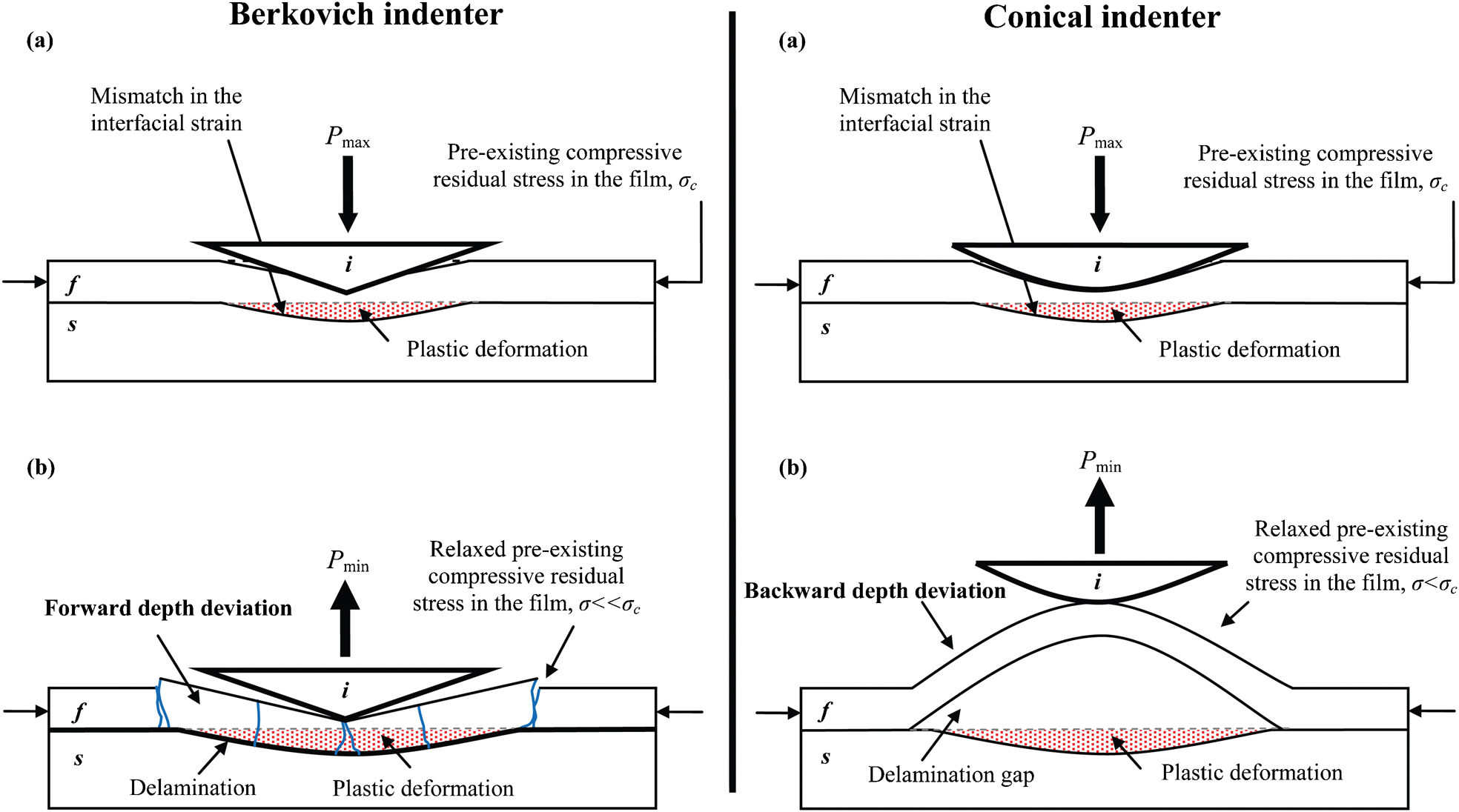
a deformation and forward depth deviation; b compressive residual stress relaxed leading forward depth deviation and fracture (for Berkovich indenter) and backward depth deviation and delamination (for conical indenter)
The above investigation indicates that a qualitative measure of the coating quality can be benchmarked, e.g. to investigate the influence of coating process and design (film thickness, residual stress and film–substrate properties) using analysis of residual impression after multiple load cycle nanoindentation.
P–h profile
During multiple load cycles of indentation, the elastic stresses caused by the indenter (tensile around the indenter contact, shear and compressive below the contact) can initiate film failure from pre-existing flaws or flaws induced by indentation itself.1,2 Similarly, during the unloading cycle, relaxation and mismatch in the indentation induced elastic stress field of the film/substrate system can delaminate the thin film from the substrate. Apart from film failure due to the elastic stress field1,2 during multiple load cycle indentation, a pre-existing residual stress (e.g. compressive in the DLC film) can affect the mechanical performance (such as fatigue strength, delamination, fracture toughness and wear resistance), which influences the reliability and lifetime of DLC components. 37 It is anticipated that loading stress can trigger the interfacial delamination of film when the film contains compressive residual stress.14,18,19 The release of residual compressive stress in the film leads to film delamination along the interface due to mismatch of the interfacial strain.14,18,19
The typical P–h profiles shown in Figs. 1,2 and 4 provide some insight into the mechanisms of film failure. As shown in Figs. 1c(ii) and 5a, significant film cracking (including interfacial delamination) was observed for the Berkovich indenter, and the P–h profile shows a forward depth deviation during all cycles of indentations. It should also be noted that a regular occurrence of ‘pop-in’ during the last stage of each loading cycle (Fig. 4a) represents significant film and substrate cracking but during later stages of cycles. This has been investigated by Jungk et al. 38 in a study related to the fracture behaviour and toughness of tetrahedral amorphous carbon films deposited on Si substrates. They suggested that ‘pop-in’ displacement excursion events during loading can be attributed to film cracking at lower loads.
For the conical indenter (Figs. 2,3 and 4, and Table 2), the P–h profile shows a forward depth deviation during all cycles of indentations, except for the load range (1–10 mN), where the P–h profiles show backward depth deviation. To comprehend the mechanics of indentation1,2 in a residual stress free (pre-existing) film–substrate system, Fig. 7 shows representative examples of contour maps of the elastic stress field during indentation using the conical indenter. These stress fields were computed by an axisymmetric finite element method (FEM) using a commercially available software (ABAQUS v6·9-2) with the assumption of perfect bonding at the film/substrate interface. The system geometry and material parameters were taken from the sections on ‘Experimental’ and ‘Results’ for the film, substrate and indenter. A comparison of Fig. 7a and b indicates that the maximum stress (von Mises) is within the film at 1 mN load but starts shifting towards the film/substrate interface for 10 mN load. This shift in maximum subsurface stress field can lead to interfacial strain and delamination without surface cracking. Although the above model does not include plasticity or any defect within materials and assumes residual stress (pre-existing) free film perfectly bonded to the substrate, it provides an estimate of the elastic stress distribution to mimic the experimental results. Based on this model, it is expected that at loads <1 mN, the behaviour during indentation will be dictated by the film properties, whereas loads >10 mN will indicate a response dominated by the substrate. Hence, only forward deviation was mainly observed in these loading ranges. However, in the load range of 1–10 mN, the properties of the film/substrate interface will dictate the nanoindentation response, and hence, backward deviation was observed for measurements in this loading range due to the dominant role of film delamination caused by the maximum stress field near the film/substrate interface. This behaviour of backward depth deviation limits the use of the method of Oliver and Pharr 8 to measure the hardness and elastic modulus under these conditions.
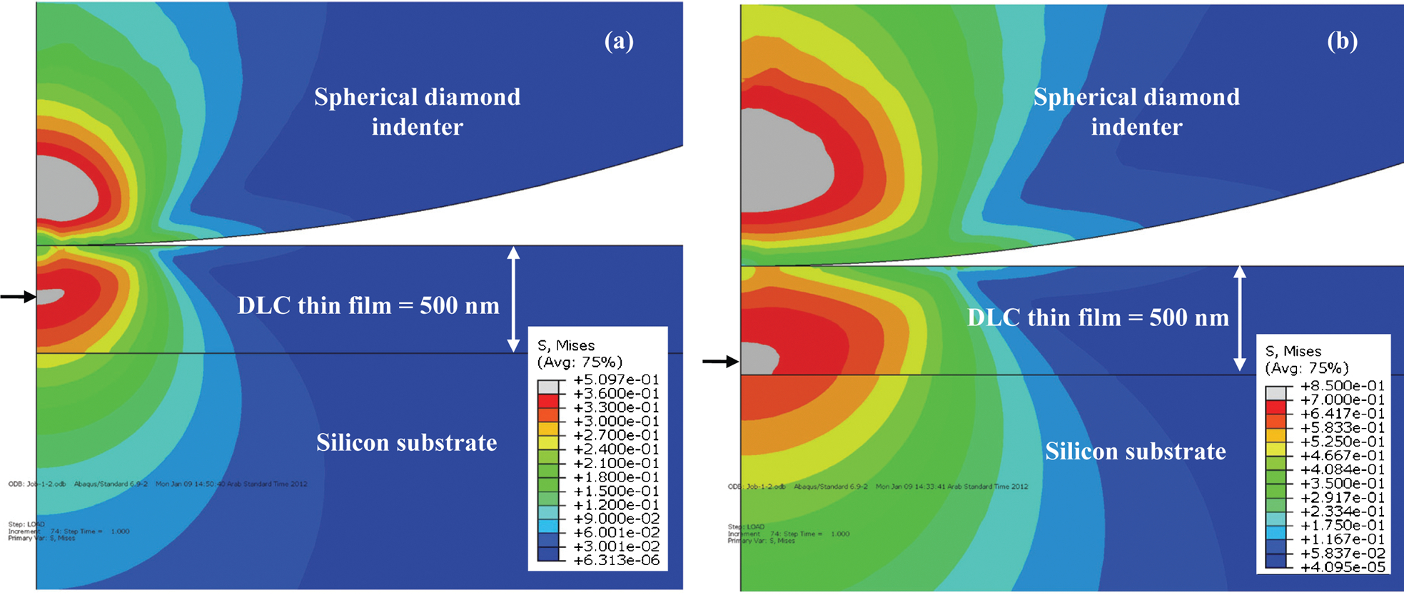
a 1 mN load; b 10 mN load
Based upon the P–h profile and AFM surface observations, the indentation cycle can be summarised (Fig. 8) in three types: (1) type I: forward depth deviation with (PL>PU) indicating elastic–plastic deformation response and film cracking (Fig. 8a); (2) type III: neither forward nor backward depth deviation with (PL = PU) indicating an ideal elastic deformation response (Fig. 8b); and (3) type II: backward depth deviation with (PL<PU) due to push-up force (Fig. 8c) in the delaminated thin film (i.e. through release of some pre-existing compressive residual stress 17 ). Also indicated in Fig. 8c are the final displacement (hf>0) and the corresponding residual forces (Pf>0). This schematic is based on the results for backward depth deviation (P–h profile at load range 1–10 mN for conical indenter, an example shown in Fig. 9). It should be noted that the measured residual co-ordinates (hf = 1·749±3·268 nm, Pf = 0·735±0·627 mN), were always greater than zero for all the four runs for backward depth deviation examples, which is an indicator of a push-up force to the indenter. This is opposite to the results for forward or no depth deviations (Figs. 1,2 and 4) and schematically shown in Fig. 8a and b.
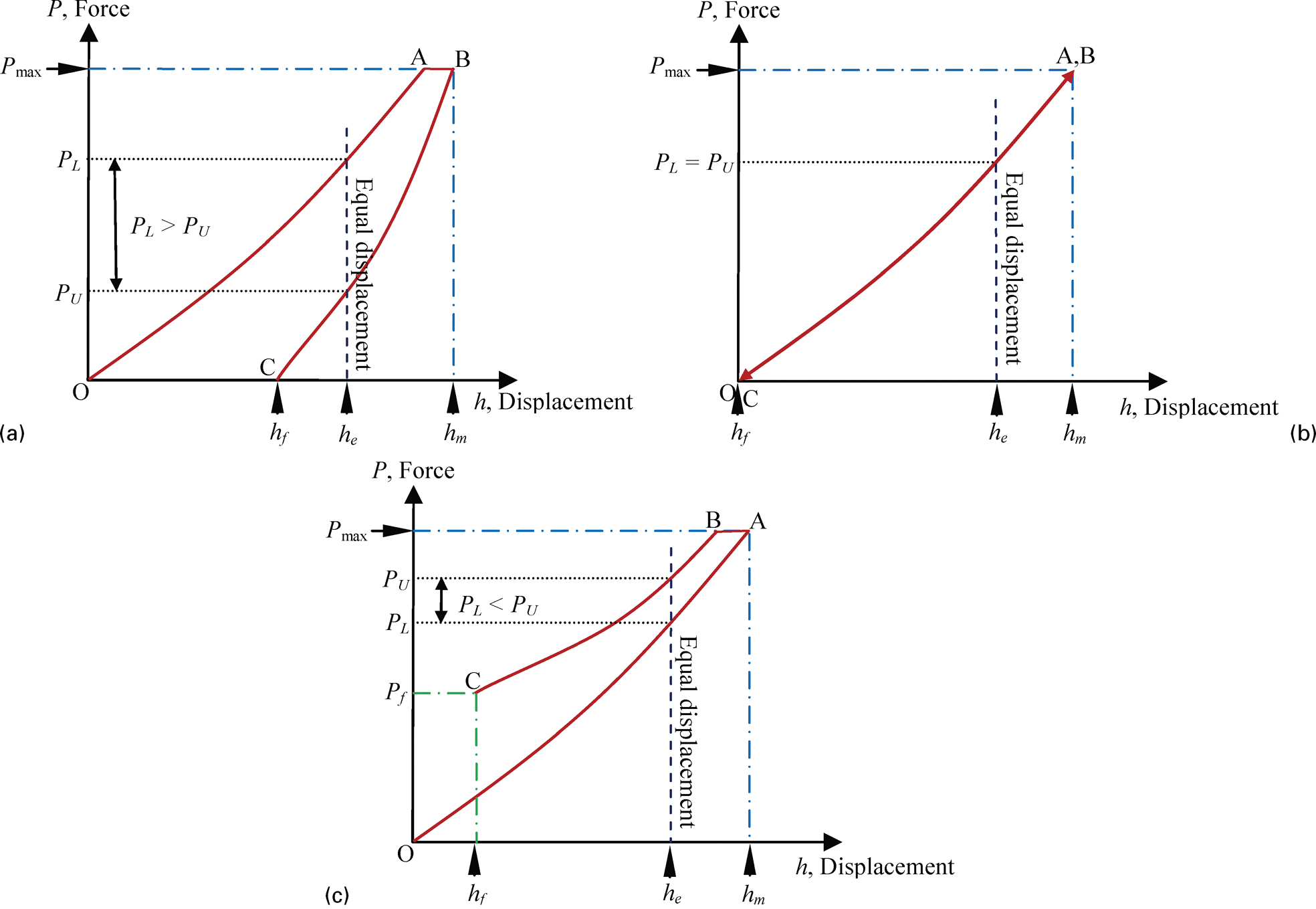
a type I: forward depth deviation with (PL>PU) indicating elastic-plastic response with hf>0 and Pf=0; b type II: neither forward nor backward depth deviation with (PL<PU) indicating elastic response with hf=0 and Pf=0; c type III: backward depth deviation with (PL<PU) due to push-up force from delaminated thin film with hf>0 and Pf>0
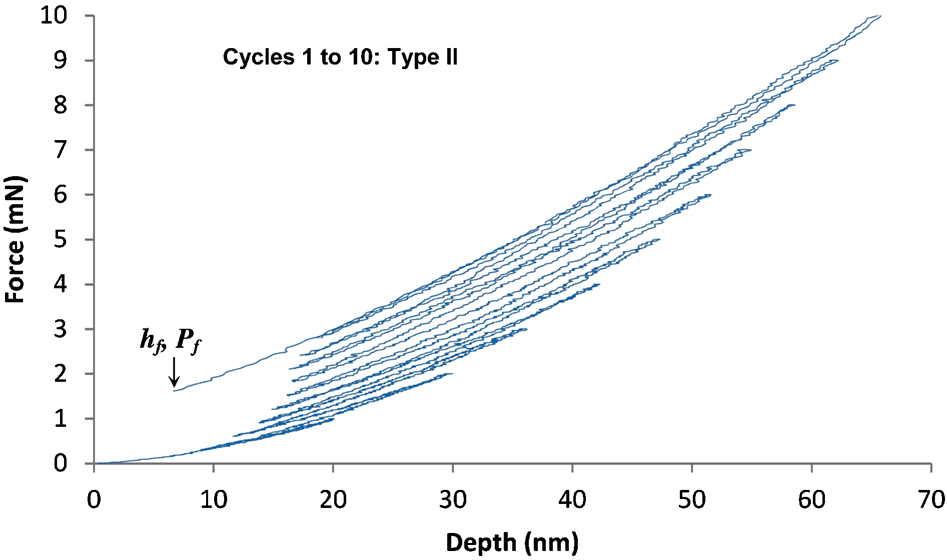
Multiple load cycle nanoindentation (conical indenter) full record of force–displacement measurement at load range 1–10 mN indicating backward depth deviation: hf = 6·65 nm is final displacement, and Pf = 1·60 mN is corresponding residual force
There was also a regular occurrence of ‘pop-in’ during the last stage of each loading cycle and pile-up [Fig. 4(ii)], and an indication of film cracking (inner ring cracks, surface radial cracks and delamination) and substrate cracking during the later stages of cycles. These have been investigated by Ikeda et al. 39 on nanocrystalline diamond (NCD) film coated SiC substrates to detect and separate the outer and inner ring cracks using acoustic emission (AE) techniques during conical nanoindentation. They suggested that the delamination of NCD films was caused by mode II fracture or buckling of the film. They also suggested that the higher number of ring cracks was attributed to the weak intergranular cohesive strength of the diamond film, whereas the few surface radial cracks in the NCD film were found to be due to the difference in compressive residual stresses. However, von Stebut et al. 40 have suggested that the Hertzian shaped ring cracks 41 developed through the film thickness may not always propagate, further leading to delamination from the substrate as demonstrated on various thin films by Ikeda et al., 39 Tsukamoto et al., 42 Amraval et al., 43 Belmonte et al. 44 and Fan et al.45,46
In the present investigation under the Berkovich indenter (100–200 and 50–500 mN) and conical indenter (50–500 mN), when the penetration depth is greater than the film thickness, some sharp appearance of ‘pop-in’ events during the later stages of the last few loading sections were observed, e.g. Figs. 1b(ii) and 4a. These ‘pop-in’ can also be attributed to phase transformation in silicon substrate apart from film and substrate cracking. 4 A more gradual ‘pop-out’ event5,31 was observed for some of the runs under the Berkovich indenter (10–100 mN) and conical indenter (100–200 mN) during the final unloading section, typically before the thermal drift section of the test is reached. This ‘pop-out’ can be attributed to a small amount of phase transformation in silicon substrate,4,5,31 but further investigation is required to confirm if this is due to cracking or phase transformation. Studies of this nature in the future can be performed by incorporating AE sensors and data recording during the multiple load cycle nanoindentation routine, where it may be possible to distinguish between the AE signals caused by cracking or phase transformation. 2
Considering different types of failure during nanoindentation, a thin film with higher adhesive strength and a controlled pre-existing residual stress are required for the durability of the coated components. Nanoindentation test can be used to obtain a better understanding of the degradation mechanisms and behaviour in thin films. This is not only important for the purpose of simulating the performance of thin films in low cycle contact conditions, but a better understanding of the deformation and cracking mechanisms may lead to a better understanding of the fatigue performance and wear mechanism in more complex conditions (e.g. particle impact, rolling or sliding contact at nanoscales).
Conclusions
The main conclusions drawn are as follows:
The geometric shapes of the indenter test probe (Berkovich or conical) and indentation load range were critical in inducing localised indentation cyclic stress, leading to distinct film failure mechanism.
Based on the depth deviation in the P–h profile (during holding and unloading stages), and supplemented by AFM topographic observations and FIB imaging of indentations, two types of film failure mechanisms were observed. The failure of films starts from cohesive failure via interfacial film delamination, resulting in backward depth deviation for the conical indenter in a particular load range (1–10 mN), whereas forward depth deviation for the conical and Berkovich indenters at all the other load ranges.
The film delamination failure during indentation indicated release of elastic stored energy (pre-existing compressive residual stress) and can be indicated through backward depth deviation (during holding and unloading stage) for the conical indenter.
Although it is difficult to state that a particular load range during indentation can induce forward depth deviation (type I), neither forward nor backward depth deviation (type III) or backward depth deviation (type II) in P–h profile, a simple FE model indicates that the location of maximum stress (von Mises) near the film/substrate interface can indicate backward depth deviation using conical indenter. Other film properties such as localised adhesive strength, through thickness residual stress profile and microstructure also need to be considered for improved indentation modelling.