
Abstract
The relationships between microstructure and plastic flow properties of copper single crystals deformed at low temperatures are reviewed based on the analysis of experimental results of mechanical, structural and electrical resistivity characterisation. Electrical resistivity measurements suggest that the flow stress correlates with the average density of defects accumulated in the microstructure. The characteristic microstructural length scale that determines the flow stress corresponds closely to the size of dislocation free channels and/or cells produced during plastic flow. The correspondence between micro- and macroscopic approaches to the plastic flow has been analysed based on the behaviour of dislocation mean free path and mean slip distance and their relationship to the microstructure. Production and annihilation of nanoscale debris and point defects and their role in plastic flow and questions pertinent to the influence of microstructural instabilities on the flow stress, workhardening, storage and annihilation of lattice defects have been discussed.
Keywords
Introduction
Plastic deformation is a non-equilibrium dissipative process associated with motion of lattice dislocations and their interaction with various elements of materials microstructure. The result is the development of a dense and complex network of defects that require the application of increasingly larger stress to continue the plastic flow in the process known as strain hardening. Self-organisation of dislocations in different morphologies and the effect of the microstructure on physical properties of engineering materials have been the subjects of interest since the inception of dislocation theory.1–5 In a recent article, 6 Brown has considered these processes from the perspective of self-organised criticality (SOC) and has outlined consequences that SOC theory offers in understanding plastic deformation of materials. Various aspects of plasticity have been discussed including properties of dislocation sources, collective motion of dislocations, formation and properties of slip bands, dislocation strengthening, the mean free path theories and others. The intermittent nature of dislocation flow that occurs irregularly in the form of jumps between metastable configurations and the organisation of dislocations that leads to the critical behaviour have been analysed by considering the relationship between the obstacle controlled plastic flow and the strain hardening and the role of the cross-slip in this process.
While many of the results available in the literature follow the outcome of SOC, Brown acknowledges that there are complications, or even controversies, related to certain aspects of the plastic flow. For example, as mentioned above, the role of cross-slip in strain hardening and pattern formation, understanding stage III, understanding twinning deformation and the link between processes occurring across length scales. The purpose of this article is to discuss some of these issues with the focus on the relationship between the microstructure and the mechanical and the electrical properties of copper single crystals deformed at low temperatures.
The structure of this article is as follows. We start by considering macroscopic geometry of crystal deformation to emphasise the role of external stress coupled with the orientation of the lattice in selecting the dominant slip systems and the consequences to the flow pattern, the microstructure and the workhardening when the change of dominant slip occurs. Observations of the nature of slip in single crystals at advanced deformation and studies of the microstructure will allow correlation of localised slip with the appearance of stage III at low temperatures. By analysing the microstructure, we find that it contains not only dislocations but also a very high density of nanoscale debris that exceeds the density of former defects. This smallest component of the dislocation substructure, hidden in a background of dislocations, has rarely been included in any considerations of the workhardening and is not incorporated in the existing strengthening models. We discuss briefly its nature and argue that, due to their high densities, these small defects may play an important role in blocking the slip. Further, we discuss some outstanding, yet fundamental questions pertinent to the types of defects that are produced during plastic flow, including the origin and the type of point defects, properties of fine debris, influence of point defects and fine debris on the flow stress, the contribution of nanoscale debris to the workhardening and the microstructure evolution. To explore these questions, we carry out analysis of electrical resistivity measurements on high purity copper single crystals at 4 K, to understand the influence of different types of defects on the strengthening relation. The results indicate that including the total defect content produces a relationship with the strengthening coefficients falling in the range of values expected for the hardening processes controlled by the forest interactions. The self-consistency of these results is tested against the macroscopic workhardening properties by examining the behaviour of dislocation mean free path and mean slip distance obtained by two independent approaches. It will be evident that, while two variables exhibit overlaps within stage II of workhardening, they diverge during stage III in single crystals. This affords the opportunity to assess the correspondence of micro- and macroscopic models in describing microstructure evolution of crystals at 4 K.
The analysis is carried out based on the data published in the literature on copper single crystals oriented for single and multiple slips with <541> and <100> orientation of the tensile axis deformed at 4 K. Some previously unpublished results of optical microscopy and TEM observations are also presented. The mechanical twinning that occurs in <541> orientation at high stresses is not discussed here. We hope that the results will enhance understanding of plastic flow in single crystals at low temperatures and its relationship to the strain hardening.
Geometry of crystal deformation and intermittent slip
Single crystals with orientation of the tensile axis from the middle of the stereographic triangle deform by dominance of one slip system, which, depending on the exact orientation of the crystal, accounts for 75–90 of a global slip. 7 In <541> single crystals deformed at room temperature, the primary slip system constitutes 80–90 of the total glide, and a gradual increase in the activity of the conjugate slip system is observed when the tensile axis rotates towards the <100>–<111> symmetry line and it passes <112> overshoot orientation after ∼60 of strain.
The conjugate system is dominant among the secondary slip systems, and the glide in all secondary slip systems supplies only a few per cent of total glide. Basinski and Basinski distinguish between two kinds of secondary slip. One is the ‘microscopic slip’ occurring to relieve the internal stresses produced by primary dislocations and producing slip marking patterns on the surface. Another type is ‘slip-line slip’ activated in response to the applied stress and operating typically in much smaller proportion to the corresponding resolved shear stress acting on it, which is also visible at the surface. 7 The secondary slip plays a critical role in controlling flow pattern, the evolution of the microstructure and the workhardening.
During consequent deformation, when the tensile axis rotates further towards the primary glide direction, the activity of the conjugate slip system increases steadily at the expense of the primary slip system. Eventually, the changeover of these two slip systems may occur, with the old conjugate system assuming the role of the dominant slip and the old primary system acting as the secondary slip. 7
In Cu–6 at.-Al single crystals with orientation of the tensile axis close to <112>, one observes three times a change of the dominant glide system between primary and conjugate systems during the onset of ∼70 tensile deformation. 8 The process is associated with an abrupt decrease in the global workhardening rate. Every changeover is accompanied by the rotation of the tensile axis between primary and conjugate triangles, and it occurs at the point when the local hardening rates of the dominant and the secondary slip system cross each other. The process proceeds essentially in a loop. The primary slip system develops a characteristic dislocation substructure and internal stresses and enforces the rotation of the lattice to the overshoot position. At a certain point of the overshoot when the resolved shear stress on the conjugate slip system reaches a critical value, the conjugate dislocations break through the existing microstructure and the changeover occurs. The change from primary to the conjugate slip is not homogeneous, and it proceeds locally in the microstructure in the form of shear bands propagating through the old dislocation substructure. This causes stress relaxation and rearrangement of the dislocation microstructure along the band's path. The net effect is that the shear band gets harder than the surrounding microstructure; otherwise, the deformation would localise in a band leading to failure. The hardening of the propagating band occurs by means of the forest interactions and the reactions between incoming dislocations and the existing substructure, which they penetrate. The process stabilises the shear band, and the deformation is passed onto the next softer region, which hardens in turn. This organises the slip in the form of the Lüders type front propagating through the sample, and as soon as the whole sample is being swept by the front, the homogeneous deformation is re-established. The new dominant slip system (conjugate) develops its native defect structure, which interacts with the dislocations of the old (primary) glide system. In response to these interactions, the local workhardening rate in the secondary slip system is higher than the hardening rate in the dominant slip system. 8
During subsequent deformation, the lattice rotates back to the original primary triangle, the activity of the dominant (conjugate) slip system diminishes due to decreasing resolved shear stress, the primary slip resumes eventually the role of the macroscopic slip and the primary dislocations take control over the evolution of the microstructure: the cycle starts again. Every time the changeover occurs, it takes less rotation to the overshoot position and the workhardening rates are lower than in the previous cycle, suggesting that the microstructure acquires less storage capacity as the oscillations progress. The plasticity limit is determined by the local workhardening properties. The cycles continue until the workhardening rate in either of the two competing systems drops to zero. 8
The results suggest that even at very large dislocation densities accumulated in the microstructure, the mobile dislocations differentiate between alien and native dislocation distribution. The decrease in the macroscopic hardening rate induced by the changeover of the slip systems is coupled to the transformation of the microstructure, which proceeds inhomogeneously in the form of a front propagating through the sample. This seems to be a general pattern of the plastic flow under alien distribution of dislocations.9–11
Similar effects were observed also during rolling of copper single crystals. 12 In this case, relatively small amounts of slip in a previously inactive glide system lead to significant relaxation effects in the microstructure, decrease in the workhardening rate and inhomogeneous deformation on a macroscopic scale. The estimated activation enthalpy of the rate controlling process ΔH≈0·3 eV was a factor of 2 or more smaller than the activation enthalpy during previous stages, suggesting a weakening of the obstacle structure.
Brown provided a detailed review of various functions of the secondary slip in stabilising the slip bands, formation of geometrically necessary and incidental boundaries and in maintaining the system in a state of SOC. 6 The coarse graining analysis assumes local fluctuations in the volume fraction of the obstacles within the shear bands, which enables the system to evolve out of equilibrium and return to an equilibrium state. The results mentioned above show how the macroscopic slip occurring in response to the applied stress affects the plastic flow and fits into this picture. It appears that the orientation of the crystal lattice is coupled to the operating slip and influences the amount of the secondary slip that is activated and the type of dislocation microstructure produced. The microstructure ultimately determines the workhardening properties of the system.
Plastic deformation of single crystals at 4 K encompasses some new features of the intermittent flow. In general, the extent of overshoot is smaller in materials with higher stacking fault energy and the change in the deformation mode occurs earlier, but it often leads directly to sample failure.13,14 This happens because the dislocations are easy to constrain and can not resist the forest cutting to the degree that dislocations with wider stacking fault ribbon can. As a result, lower stacking fault materials exhibit typically higher storage capacity for dislocations. The decrease in the deformation temperature acts in a similar way to the decrease in stacking fault energy, i.e. it increases the overshoot and moves the changeover point to higher stresses, extending the plasticity limit. 13 Thermomechanical instabilities caused by adiabatic heating of the sample accompanying the deformation process at 4 K at the higher strains affect both the flow pattern and the workhardening. 15 Finally, the change of the dominant operating mechanism at the first overshoot in <541> single crystals results in activation of twinning deformation rather than the conjugate slip. This has profound influence on subsequent flow stress and workhardening behaviour. 16
The onset of stage III, which occurs in <541> single crystals at the resolved shear stress of about 90–100 MPa, coincides with the enhanced activity of the secondary slip systems at the first overshoot. To illustrate this feature, Fig. 1 shows slip marking patterns formed in the sample deformed to advanced region A, before the onset of twinning at 4 K. 16 To reveal the net slip from different slip systems operating at this stage, the sample was repolished and subjected to additional small deformation of a few per cent at 4 K. The micrograph shows long and dense slip lines produced by the primary slip, dominating the surface area. On a background of the primary slip traces, one observes long shear bands approaching occasionally 1 mm in length, labelled ‘adiabatic shear’ in Fig. 1. The shear bands of this nature are formed on the surface of deformed crystals only during the onset of adiabatic deformation at 4 K, and so they are easily recognised from other slip marking patterns. They are the consequence of plastic instabilities produced by localised slip due to the softening of the microstructure occurring during adiabatic heating of the sample. Adiabatic shear bands are composed of arrangements of fine shears in the primary slip system (Fig. 1b) and they are aligned along composition planes, which on average are orientated close to the maximum shear plane of the sample; therefore, on a macroscopic scale, adiabatic bands are non-crystallographic. The conjugate slip is visible in the form of faint lines ∼50–100 μm long (Fig. 1b). The conjugate slip traces are less intense than the traces from the primary slip. One finds quite a few kink bands formed in the conjugate slip system of length exceeding 300 μm (Fig. 1a). They deviate 5–10° from the exact orientation of the conjugate plane. In some places, the conjugate kink bands arrest the propagation of the adiabatic shear bands, suggesting that they have formed earlier. Finally, one observes very dense slip marking patterns produced by the cross-slip system. Their lengths vary from fine markings to longer slip lines, extending to a distance of 100 μm or longer (Fig. 1b). It is not clear what is the origin of this kind of macroscopic cross-slip, but it is produced exclusively during stage III. It suggests that intense relaxation is taking place in the microstructure, presumably in response to the development of internal stresses possibly with the aid of the applied stress. Zaiser and Hähner have argued that abundant cross-slip is activated to reduce the fluctuations of the internal stress and plastic shear strain rate during stage II and is ultimately responsible for the appearance of the onset of stage III in fcc single crystals. 17 Present results confirm the unusual form of the cross-slip appearing during stage III in <541> single crystals deformed at 4 K. No evidence of slip traces from critical slip systems has been found at this stage, which suggests that critical slip systems contribute tiny amounts of slip to the macroscopic deformation, in agreement with Basinski and Basinski's results. 7
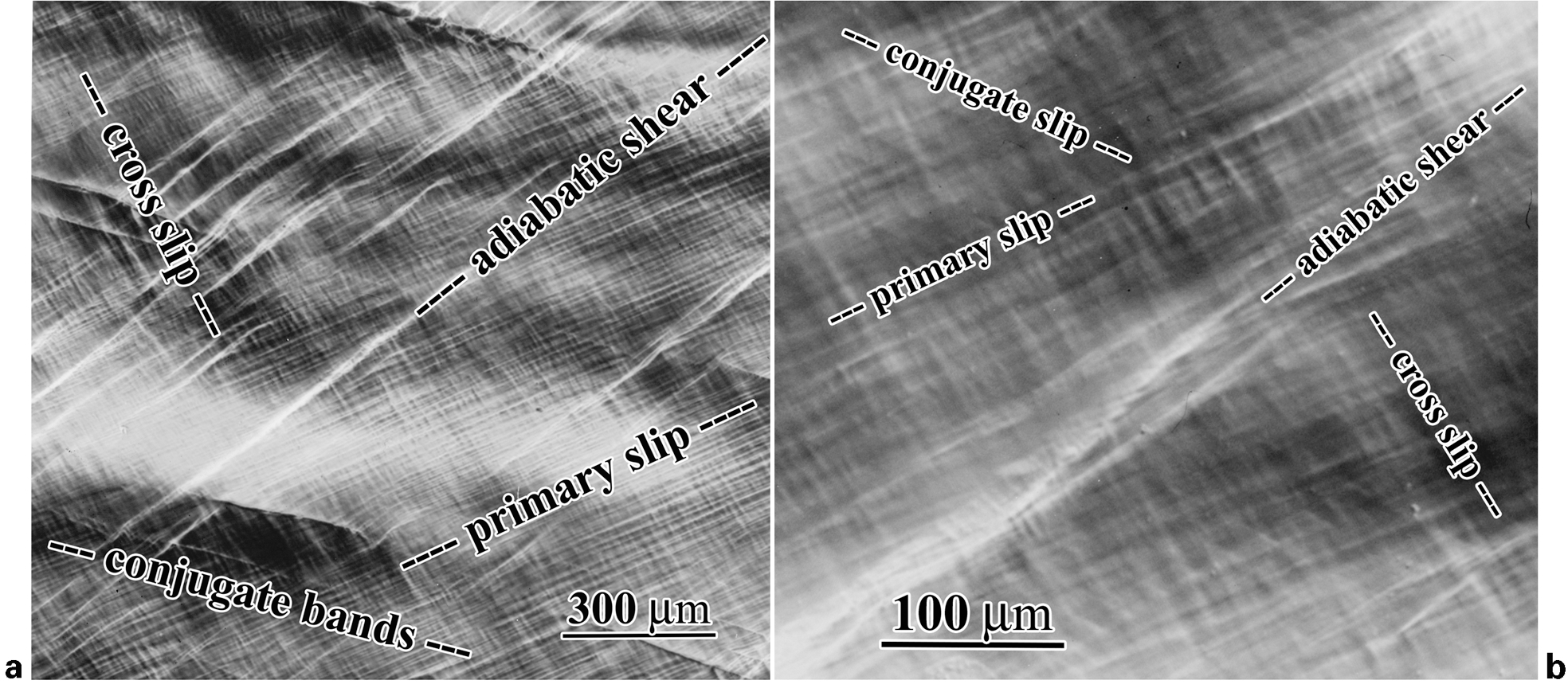
Optical microscopy observations carried out with Nomarski contrast under two different magnifications, showing slip traces formed on surface at onset of adiabatic deformation during stage III of <541> copper single crystals deformed at 4 K. Slip marking features formed by different slip systems are labelled on micrograph. Adiabatic shear bands are composed of fine shears in primary slip system and on average are orientated close to maximum shear plane of sample. Tensile axis of sample is oriented approximately horizontally, and orientation of face observed is close to (11
Brown has discussed the lack of similarity between slip marking patterns observed at the surface and the underlying dislocation microstructure formed in the bulk, a common feature of the structures produced by SOC, 6 the main reason being the temporary nature of the slip bands, which leave traces on the surface but degenerate immediately into the network of primary and secondary dislocations, losing this correspondence. Additionally, the stress state and the image forces affect the distribution of dislocations in the neighbourhood of the free surface and eliminate many dislocations, so the lack of such correspondence is not surprising in this case. 6 Nevertheless, TEM observations provide valuable insight into the spatial organisation of the slip on a different length scale and permit basic features of the corresponding microstructure to be characterised.
Figure 2 shows TEM observations of the dislocation microstructure developed in <541> copper single crystals deformed to the resolved shear stress of 145 MPa at 4 K (end of region A, just before the twinning deformation in Fig. 1c in Ref. 6). The observations in the primary glide plane in Fig. 2a reveal a complex, inhomogeneous network of defects with sheets of dislocations arranged parallel to the conjugate glide plane marked on the micrograph. Occasionally visible are dislocation free channels elongated along the trace of the conjugate plane of lengths approaching 1 μm. At the centre of the micrograph, one observes a diffuse band-like structure aligned parallel to a trace of the cross-slip plane, suggesting some resemblance to the macroscopic cross-slip lines observed by optical microscopy in Fig. 1. The band was analysed independently, and it contains three sets of dislocations belonging to conjugate, cross- and critical glide planes and a high density of primary dislocation debris. Owing to the unbalanced dislocation content, the structure develops small missorientations responsible for the observed diffraction contrast. Dense dislocation assemblies along the trace of the conjugate and critical planes with dark contrast are visible in other places of the substructure.
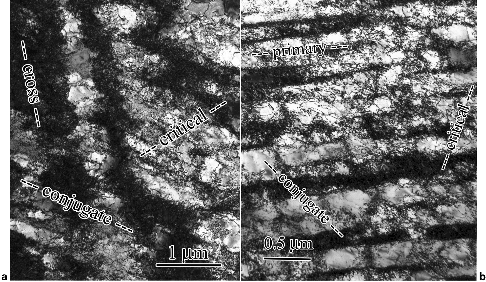
Multibeam bright field TEM observations of dislocation microstructure developed in <541> copper single crystals deformed in tension to shear stress of 145 MPa at 4 K (end of stage A): a observations carried out in section parallel to primary glide plane (11
Observations by TEM carried out in the section parallel to the cross-glide plane in Fig. 2b reveal arrangements of densely dislocated deformation bands produced by the main slip system interleaved with dislocation free channels, which in turn are separated by dislocation walls in secondary planes. The basic act of the slip in Brown's theory relies on the nucleation of the ellipsoidal deformation bands with blade-like shape and small aspect ratio, lying approximately in the glide plane. 6 One may expect that deformation bands clearly visible in the upper part of Fig. 2b, but present also in other places of the microstructure, resemble the kinds of bands Brown is referring to in his article. 6 Some of the longest primary deformation bands observed here are of lenticular shape, of length about 2–4 μm and thickness about 0·2–0·4 μm, so their average aspect ratio is estimated to be ∼10. It is conceivable that the nucleation and the spatial organisation of these bands into the macroscopic shear bands visible in Fig. 1 is linked to the occurrence of adiabatic load instabilities observed at this stage of deformation in the crystals. The bands rely on the dual role of the forest, as discussed by Brown, on the one hand, in stabilising the slip band, and on the other hand, in producing a strong obstacle structure that the primary bands must overcome to propagate through the lattice, coupled to the adiabatic load drops.
As seen in Fig. 2b, the bands are terminated by dislocation walls diffused along the conjugate or critical planes. When formed to relax stress concentrators at the tip of the bands, the secondary dislocations spread no more than beyond the thickness of one or two channels, about 0·2–0·5 μm high. Well compensated secondary walls developed earlier are oriented perpendicular to the primary bands, as visible at the bottom part of Fig. 2b. In many cases, the secondary walls deviate from the orthogonal orientation to accommodate elastic stress mismatch between the channels and the walls to allow for a compatible deformation of such heterogeneous structures. In some regions of the micrograph, for example, in the central area, bottom right corner or top right corner, the primary deformation bands are broken up and fragmented by the slip occurring in the conjugate and/or critical planes. These places are distinguished by the traces of the glide planes of secondary dislocations, which are inclined at lower angles to the primary deformation band extending across a few layers at a distance of 1 μm or longer.
Studies of the fatigue in copper single crystals have revealed that when it becomes necessary for the secondary slip system to operate as the dominant slip in the secondary fatigue samples, it rebuilds the existing microstructure to a structure characteristic of its native configuration and wavelength. This reconstruction proceeds in a highly inhomogeneous manner accompanied by the fatigue softening and the localised character of the fatigue deformation. 18 Present results show similar effects and indicate that, under monotonic deformation, the primary deformation bands can be opened up and fragmented by operation of secondary dislocation sources in a localised glide. The observations thus suggest the dual nature of the secondary slip. When it operates homogeneously, it produces hardening of the band, stabilises it against the existing microstructure and builds the obstacle structure that opposes its motion. 6 On the other hand, when it is organised as a localised slip on a scale larger than the characteristic wavelength of the microstructure, it may break up the deformation bands and create a soft path for subsequent slip.
It seems that the contribution of this kind of secondary slip to the global deformation at 4 K, in addition to intensive adiabatic load instabilities coupled to the activity of primary slip bands, provides a reason for the decrease in the macroscopic hardening rate in single crystals at large deformations. If the average slip distance increases in the microstructure as a result of local slip instabilities and inhomogeneous deformation, the workhardening rate must decrease. Therefore, the observations suggest that the localised character of the slip is correlated with the decrease in the global hardening rate of the crystals at high strains.
Brown discusses these aspects in terms of the fluctuations in obstacle density caused by dislocation avalanches, arguing that the SOC is preserved regardless of how the slip is distributed spatially, as long as the distribution is statistically unchanged during the course of deformation. 6 The dynamics and interplay of slip systems is also very important. As the experimental results show, the workhardening behaviour discriminates between the set of slip systems operating simultaneously in a homogeneous manner and operating sequentially, even though two modes lead to the same mesoscopic deformation. This is because different interactions dominate these two processes and produce a distinct microstructure, which ultimately controls the plastic flow.
Intermittent flow of dislocations, production of point defects and debris
Production of debris during plastic flow
Figure 3 shows weak beam TEM observations of the dislocation substructure in <541> copper single crystals from the end of stage A at 4 K, complementing the mesoscale observations discussed in Fig. 2. In Fig. 2, it was observed that the microstructure evolves into three-dimensional channel-like dislocation networks with lower dislocation density channels separated by dense dislocation walls formed by the accumulation of dislocations in the primary and secondary slip planes. The spatial character of the microstructure is visible in the section parallel to the primary glide plane in Fig. 3a and cross-glide plane in Fig. 3b at a higher resolution. The evolution and the defect content inside the channels and walls have been analysed elsewhere for <541> crystals deformed at 4·2 K19,20 and at 78 K. 21 It has been shown that the dislocation structure formed in the primary glide plane contains a high density of nanoscale dislocation debris consisting of primary dislocation dipoles and loops predominantly of vacancy type, vacancy type faulted dipoles, stacking fault tetrahedra (SFT) and partial SFTs and small dot-like defects. 21 These debris are visible in Fig. 3 on a background of ordinary dislocations that are stored in the walls. Burgers vector of much of the debris is traceable back to primary dislocations. 21 Well compensated and stable secondary walls are orthogonal to the primary bands (carpets) to reduce long range back-stresses arising from a difference in the elastic and plastic strains in the periodic structure of dislocation free channels and dislocation reach walls. 22 As seen in Fig. 3b, some secondary walls are not ideally perpendicular to the primary bands and show a tilt angle, which varies between 80 and 90°, suggesting that they orient in this way to accommodate diverse elastic shears between soft channels and hard walls. 22 This is achieved by the suitable arrangement of edge dislocations in the secondary slip planes and the accumulation of a large density of fine debris produced by the primary slip system (see also Figs. 3 and 4 in Ref. 20).
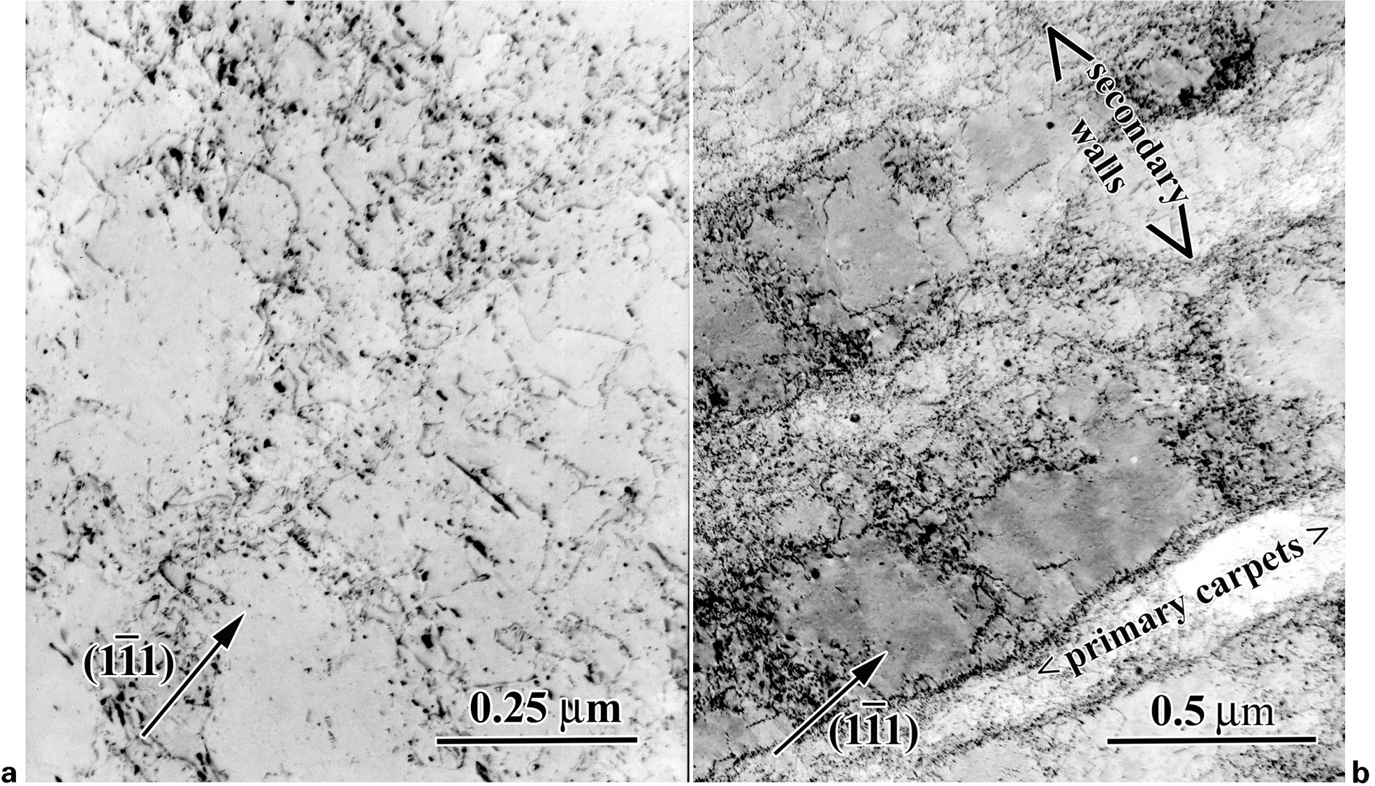
Weak beam observations of dislocation substructure developed in <541> copper single crystals deformed in tension to shear stress of 145 MPa at 4·2 K (end of stage A) complementing bright field TEM observations in Fig. 2. a section parallel to primary glide plane (11
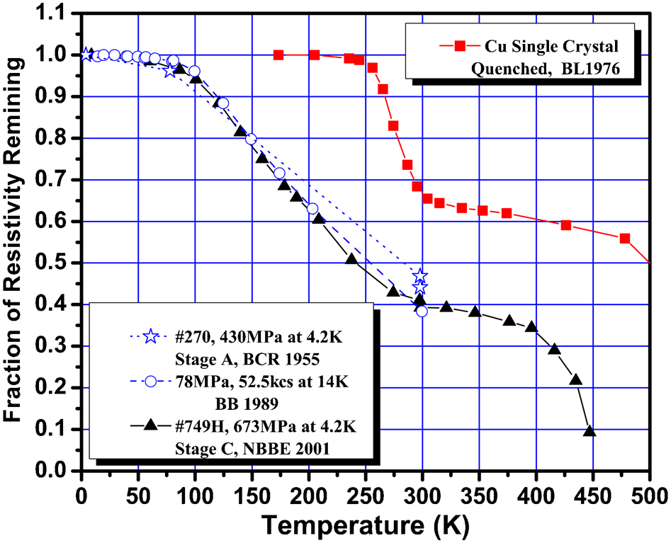
Isochronal annealing characteristics of deformation induced resistivity as function of annealing temperature for copper single crystals deformed under tension and after low cycle fatigue. Stars are results of Blewitt et al. 32 for copper single crystals, sample no. 270 with initial orientation close to <741>, deformed to shear stress τ≈150 MPa at 4·2 K (tensile stress σ≈430 MPa, stage A of deformation). Open circles represent data of Basinski and Basinski (B&B 1989) for <321> copper single crystal, fatigue at 14 K for 54·5 K cycles. 55 Black triangles are data for <541> single crystal no. 749H, deformed in tension at 4·2K to flow stress σ≈673 MPa (stage C, after twinning). 16 For comparison, isochronal annealing of quenched-in vacancies in copper single crystals are shown by squares: after Bourassa and Lengeler 54
Brown has reviewed dislocation mechanisms responsible for the progressive refinement of primary edge dipolar structures involving reactions between trapped dipoles and incoming dislocations that favour structures comprised of narrow dipoles of vacancy character.23–25 One can argue that other debris, including small SFTs and dot-like clusters, are produced by these kinds of processes and mechanisms involving conservative motion of dislocations.26–28 The evolution of the microstructure that leads to the production, accumulation and refinement of various types of lattice defects in the spatial arrangement as visible in Fig. 3 is consistent with such a description.19–21
Figure 3 reveals that dislocation debris are produced in very large quantities; they can be expected to act as obstacles impeding the motions of dislocations influencing the workhardening, flow pattern and the microstructure evolution. They have rarely being included in the plasticity models and Brown's article is an important step in this discussion. However, the substructure in Fig. 3 contains only about 40 of defects that were actually produced at this stage at 4 K.16–20 Correspondingly, 60 of deformation induced defects anneal out during heating up to room temperature. Debris of sizes smaller than about 2–4 nm that are below the resolution of the weak beam technique are invisible on the micrographs, and their presence cannot be confirmed based on TEM observations. 29 Nevertheless, after inspecting Fig. 3, it is legitimate to think about the nature of defects that anneal out and their relationship, if any, to the fine debris that are stored in the microstructure. In the following, we discuss briefly these aspects.
Production of self-interstitials and interstitial dipoles during plastic flow
There have been long discussions in the literature about the nature of recoverable defects in deformed metals, beginning with the work of Molenaar and Aarts 30 and Druyvesteyn and Manintveld 31 followed by the seminal work of Blewitt et al.32,33 on copper single crystals and other metals. 34 Basic geometrical arguments suggest that during plastic deformation interstitial ions should be produced in larger quantities than vacant sites,35–37 in which case the rearrangement of interstitials should be detectable with suitable apparatus. However, various experimental studies carried out with independent techniques such as hyperfine spectroscopy,38–42 positron annihilation,43–46 electrical resistivity,16,32,33,47–50 calorimetry 51 and electron microscopy,20,26,28,52,53 suggest that interstitial type defects are not stored in the substructure of deformed metals.
To illustrate this feature based on electrical resistivity results, Fig. 4 shows compilation of the isochronal annealing characteristics of copper single crystals oriented for easy glide deformed under tension and by fatigue at low temperatures. For comparison, the isochronal annealing curve of quenched-in vacancies is also included in Fig. 4. It is seen that quenched-in vacancies start to anneal out above 250 K, with the activation energy of ∼0·75 eV corresponding to stage III recovery in copper. 54 At room temperature about ∼35 of quenched-in resistivity anneals, followed by the next recovery stage (stage IV recovery) above 475 K. 54
The annealing of deformation induced defects shows different properties. Holding an unloaded sample for ∼6 h at 4 K does not produce measurable changes in electrical resistivity, which indicates that elastic interactions do not induce defect rearrangements and annihilations at low temperatures. 16 Less than 1 recovery of resistivity is observed below ∼60 K where one would expect annealing of interstitial ions. Very little, 4–5, resistivity recovery occurs at 100 K, whereas above 100 K, resistivity recovers continuously up to room temperature with ∼40 of initial deformation induced resistivity remaining in the sample. It appears that isochronal annealing of tensile deformed crystals16,32 shows excellent agreement with fatigue single crystals, as reported by Basinski and Basinski 55 (Fig. 2). The results indicate that resistivity recovery follows the same characteristic independent of degree of deformation or deformation mode (fatigue or tension). Early recovery studies of noble metals deformed at 4 K confirm these observations. 56 One concludes, therefore, that electrical resistivity data (and other techniques for that matter) do not give support to the notion of interstitials being produced during plastic deformation in these crystals.
It is still possible that interstitial ions or clusters of interstitials are produced but are removed by mobile dislocations or annihilated with vacancy complexes shortly after they are born and therefore are undetectable by standard techniques.57,58 Recent molecular dynamics (MD) studies suggest that small sizes of stable interstitial loops are produced during deformation of Al, and that they contribute to the strengthening. 59 However, MD simulations suffer from various shortcomings related to inaccuracies of atomic potentials, time scale discrepancies, fine size of the models, boundary conditions and issues related to proper identification of defects in a highly distorted atomic structure. It would be valuable to see if similar results can be obtained with other atomic potentials and simulation conditions. As for now, we conclude that apart from limited MD results, no definite experimental evidence, direct or indirect, for interstitial production and annihilation has been reported for metals.
Different arguments apply to the interstitial dipoles or interstitial loops (prismatic loops of interstitial type). 6 In an array of perfect dislocations, interstitial and vacancy dipoles are expected to coexist roughly in the same numbers. Various TEM observations presented over the years suggest imbalance between the number of vacancy type perfect dipoles and the interstitial dipoles stored in the structure. For example, in copper single crystals fatigued at room temperature, Antonopoulous et al. observed twice as many vacancy as interstitial dipoles. 52 On the other hand, Tippelt and co-workers 60 found only a small primacy of vacancy over interstitial dipoles in nickel single crystals fatigued at 600 and 750 K. Nabarro and Brown have discussed this issue and showed that, in an open dislocation array, interstitial dipoles can easily be replaced by vacancy dipoles by exchanging partners with other dipoles with the aid of screw dislocations.61,62 The transformation is driven by the lower energy of narrower vacancy dipoles, which may occur during sample unload if the dipole is connected to the mobile screw dislocations. The model provides the rationale for the natural selection of vacancy dipoles over the interstitial dipoles and the evolution of the dipole structure towards finer and narrower debris of vacancy type and is consistent with observations.
Production of vacancies during plastic flow
The recoverable component of deformation induced resistivity has been commonly credited to the annihilation of vacancies produced during deformation. Figure 4 indicates that a major fraction of deformation induced resistivity that disappears between 4 K and room temperature cannot be attributed to the annihilation of single vacancies. Deformation induced defects anneal at lower temperatures with smaller activation energies; at 250 K, where vacancies are just becoming mobile, 50 of the deformation induced resistivity has already disappeared. There is no clearly defined annealing stage as observed in quenched-in resistivity data (Fig. 4). On the contrary, the defect species annealing out between 100 and 250 K have a spectrum of activation energies in the range of about 0·2–0·8 eV. This suggests that mechanisms such as pipe diffusion and/or volume diffusion of multivacancy clusters control the annealing process. 16 Polák has observed qualitatively similar isochronal annealing characteristics in copper single crystals fatigued at 78 K. 63 In his case, the stage III recovery was more pronounced than that observed in Basinski and Basinski's studies, 50 suggesting that defects, which anneal above 250 K, are produced in larger quantities during fatigue at 78 K than at 4 K. Polak interprets these results as evidence of the higher rate of vacancy production at 78 K as compared to 4 K. 64 Basinski and Basinski observed a transition in persistent slip band (PSB) morphologies between 250 and 300 K from triangular bulges formed below 250 K to non-bulged PSBs with intrusions and extrusions formed above 300 K, but have argued that there is no evidence of point defect involvement in formation of such PSB structures. 65 Single crystals fatigued at room temperature show no recovery of resistivity up to ∼360 K and small annealing effects at higher temperatures, which have been interpreted in different ways by various researchers.63,66
Pipe diffusion has long been known to be the mechanism controlling destabilisation of narrow dislocation dipoles and dipole annealing in crystals.67–70 More recently, Matsukawa and Zinkle 71 recorded the migration of a small vacancy loop along the dislocation line in deformed gold and determined its migration energy, ∼0·22 eV. This sort of process may already be active at low temperatures and be responsible for removing part of the fine debris from the structure. Other debris may disappear by leaking vacancies through the network of pipes or the emission of vacancy clusters and their diffusion to the other defects or the surface, or, in the case of dipoles, by exchange of vacancies between dipoles of vacancy and interstitial type. 6
Careful inspection of Fig. 2 reveals that isolated dislocations and in particular sessile faulted dipoles and SFTs present in the structure are decorated with small dot-like features, suggesting that they indeed may act as sinks absorbing some other defects from the microstructure. The point can be made that annihilation and rearrangement of a broad spectrum of dislocation debris with the wide range of activation energies between 0·2 and 0·8 eV, which include small loops, faulted and unfaulted dipoles of various heights, small SFTs and SFT products and point defect clusters, can account for the recovery results observed in the electrical resistivity experiments and be consistent with the general description of the deformation process, which assumes progressive refinement of the microstructure during plastic flow.16,20,66
It is not clear what is the role of recoverable debris in the hardening process. In the analysis of this process, attention must be given to the density of lattice defects, the workhardening response and the evolution of the microstructure. Deformation experiments with intermittent annealing to room temperature show that, during region A of deformation discussed here, the sample anneal induces a small yield point after reload in addition to a small decrease in the yield stress. This is clearly visible by inspecting Fig. 5, which shows amount of yield stress recovery in <541> single crystals as a function of recoverable resistivity. The data include stress recovery effect observed in regions A and C of deformation. 16 It is seen that the flow stress recovery is roughly proportional to the density of debris removed. At the end of region A of deformation, the yield stress at 4 K recovers by <3 upon annealing of samples at room temperature. After the onset of twinning (region C of deformation at 4 K), 16 the stress recovery effect is slightly higher, and it amounts to about 4–5 of stress decrease at 60 of recovered defects, as shown in Fig. 5. In other words, after removing 60 of deformation induced defects from the microstructure, the yield stress decreases by <5 of its nominal value before annealing. 16 This indicates that also in the twinned structure, known to produce a substantially larger fraction of recoverable debris than untwinned material and containing a very high density of unrecovered debris,16,20 the effect of annealable debris on the flow stress is not large, considering that the significant fraction of debris has been removed. Recoverable defects have no other influence on the flow stress, consistent with the results available in the literature.16,32,48
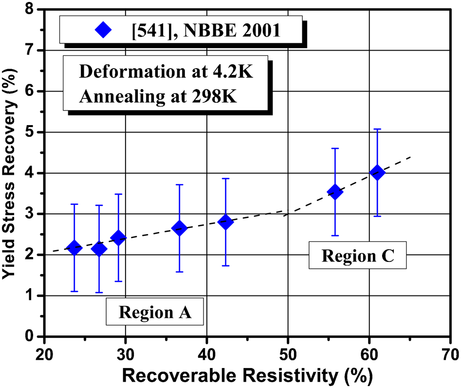
Shear yield stress recovery as function of recoverable resistivity for <541> copper single crystals in regions A and C of deformation evaluated based on measurements by Niewczas et al. 16
At the conclusion of this section, we submit that the results of electrical resistivity measurements discussed above and other results suggest that single vacancies are not produced in copper single crystals subjected to monotonic or fatigue deformation at low temperatures in quantities that would influence meaningfully workhardening behaviour. Defects annealing out at low temperatures with small activation energies that constitute the recoverable fraction of deformation induced defects are presumably residuals of larger debris refined down to these dimensions, which may contain various sizes of vacancy clusters. Results from TEM show that nanoscale debris are produced in very large quantities and are basic components of the network and all kinds of dislocation morphologies. Their origin, atomic structure, stability and their role in the plastic flow should be examined critically by carefully designed experiments and modelling studies on various materials systems.
Dislocation strengthening in single crystals at 4 K
In this section, we analyse the relationship between the flow stress and the dislocation density based on compiled results of the in situ measurements of electrical resistivity during deformation of high purity single crystals of copper at 4 K. At low temperatures, phonon scattering is negligible, and the scattering of conductive electrons from lattice defects can be measured in a precise way. The scattering of electrons on dislocations arises from high angle scattering by the dislocation core, and the radius of the scattering cross-section is about one Burgers vector; therefore, conductive electrons probe even the highest densities of defects accumulated in the crystal. 72 In situ measurements of electrical resistivity provide information about the total defect content during instantaneous deformation. The technique does not differentiate between defect species or defects that are recoverable or non-recoverable. Subsequent annealing studies have to be carried out to obtain this information. Even then, the results may be subjected to different interpretations, as discussed in the section on ‘Production of vacancies during plastic flow’. However, it is very informative to analyse data from electrical resistivity measurements from the perspective of the strengthening arising from the contribution of all defects produced during plastic flow at 4 K and to isolate the effect of recoverable and unrecoverable component of deformation induced defects on the flow properties. The key outcome of such analysis is that the flow stress scales with the total density of defects produced during plastic flow at 4 K and that recoverable defects have very little influence on the flow stress.16,48
Figures 6 and 7 show the compilation of results of in situ electrical resistivity measurements during tensile deformation of copper single crystals at 4 K.16,48 Basinski and Saimoto's results (BS 1965) are plotted as continuous curves following their data in Ref. 48. Results of Niewczas et al. (NBBE 2001) and Niewczas and Embury (NE 1999) are shown as discrete points, as obtained in the experiments.16,73 The dislocation density has been obtained from electrical resistivity assuming that all defects are dislocations and using cD = 1×10⁻²⁵ Ω m3 for specific scattering of electrons on the unit length of the dislocation line. Figure 6 shows resolved shear stress on the primary slip system as a function of dislocation density for copper single crystals oriented for easy glide during stage A of deformation. The hardening stages, stages I–III, within region A of deformation are marked on the figures. The data points are fitted to the strengthening relation τ = αsμ
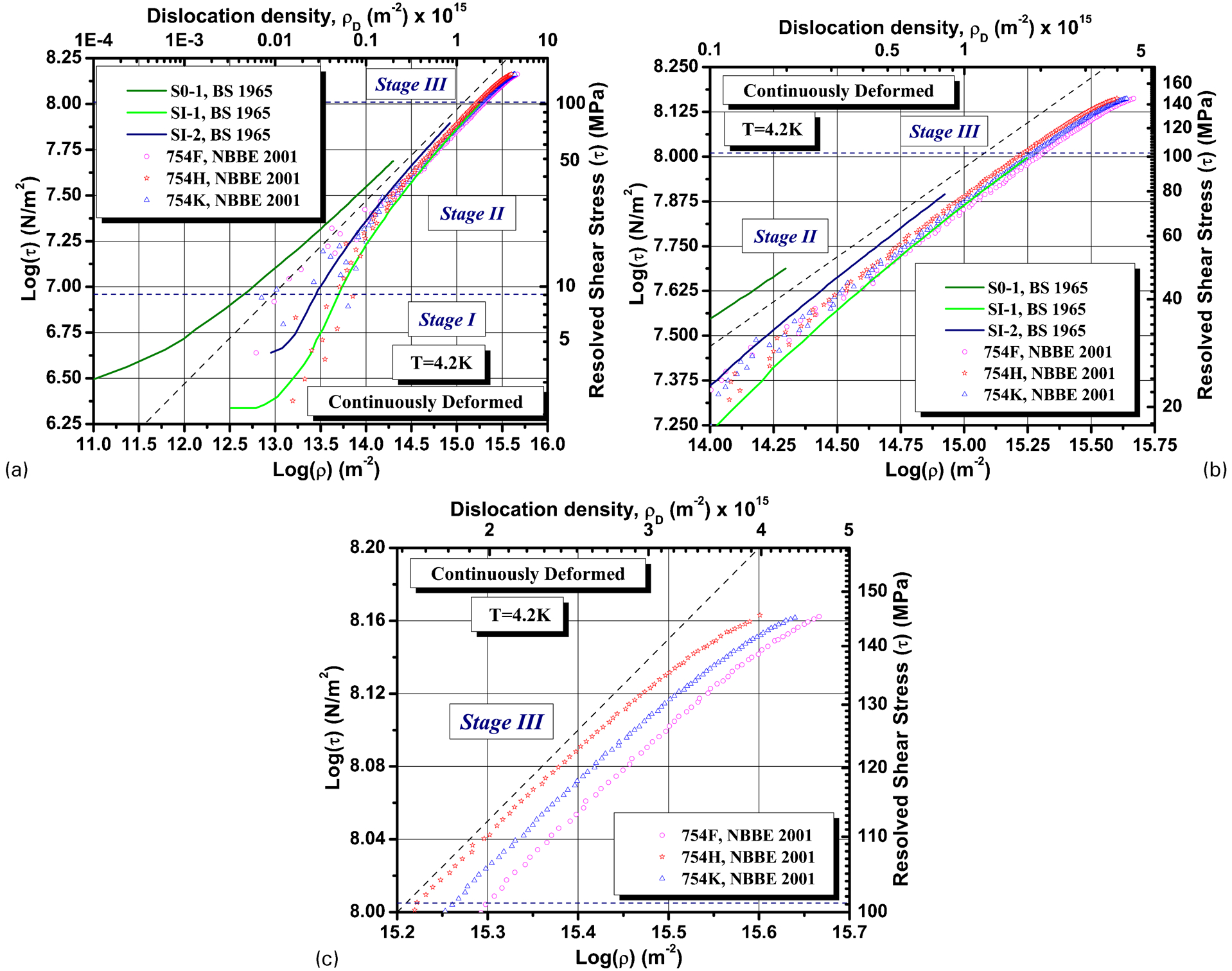
Resolved shear stress as function of total dislocation density for copper single crystals oriented for easy glide, deformed continuously at 4·2 K. BS 1965 represent different samples measured by Basinski and Saimoto, 48 NBBE 2001 are measurements carried out on three different single crystals from 754 series by Niewczas et al. 16 Dislocation densities are calculated from electrical resistivity data using specific resistivity per unit length of dislocation line 1×10⁻²⁵ Ω m3. 72 a full range of stresses during region A of dislocation glide at 4 K, b range of stresses above 20 MPa and c range of stresses above 100 MPa. Black dashed line provided for eye guidance represents one-half slope of the log (τ)–log (ρ) characteristics. Hardening stages, stages I–III within region A of deformation, are marked on graphs. Sample data are given in Table 1
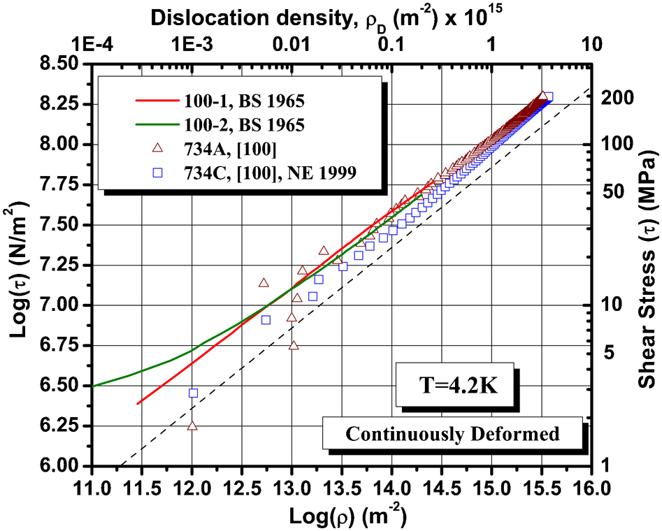
Shear stress as function of total dislocation density for <100> copper single crystals, deformed continuously at 4 K. BS 1965 and NE 1999 represent measurements by Basinski and Saimoto and Niewczas and Embury on <100> copper single crystals.48,73 The dislocation density is obtained from electrical resistivity using 1×10⁻²⁵ Ω m3 for specific resistivity per unit length of dislocation line in Cu. 72 Black dashed line provided for eye guidance represent one-half slope of log (τ) = f[log (ρ)] characteristic. Sample data are given in Table 1
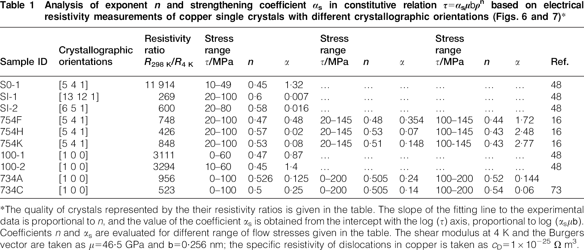
*The quality of crystals represented by the their resistivity ratios is given in the table. The slope of the fitting line to the experimental data is proportional to n, and the value of the coefficient αs is obtained from the intercept with the log (τ) axis, proportional to log (αsμ
It is seen that, at low flow stresses corresponding to stage I, both BS 1965 and NBBE 2001 data deviate significantly from the one-half slope of the dashed line marked on the figure, affecting values of the strengthening coefficient αs (Table 1). At very low defect densities, the measurements are influenced by the effect of impurities and sensitivity of the apparatus, which must be capable of measuring small changes in the potential drop with the accuracy >10−9 V. Basinski and Saimoto 48 had shown that the lower purity crystals exhibit higher rate of resistivity increase during stage I and early stage II of deformation; this effect is clearly visible in the behaviour of their samples S0-1, SI-1 and SI-2; the behaviour of crystals from 754 series also follows this trend. 16 Thus, the resistivity data suggest that dislocation–impurity interactions dominate stage I in crystals SI-1, SI-2, 754F, 754H and 754K, and these crystals exhibit faster rate of stress increase than cleaner crystals SO-1.
In a model fcc system, dislocation dynamics simulations suggest that forest interactions between collinear superjogs and incoming primary dislocations determine the hardening rate and are responsible for development of the substructure characteristic of stage I.74,75 Resistivity data in Fig. 6 cannot validate these results, but Veyssière and co-workers found no evidence that this process dominates workhardening behaviour in stage I of Al, Cu and TiAl single crystals based on their TEM observations. 76 More experimental studies are required to settle this point.
Beyond stage I, the scattering from impurity atoms is negligible compared to the scattering from lattice defects. For 754 crystals, the resistivity data fitted over the broad range of stresses between 20 and 145 MPa within the region A of deformation (at ∼145 MPa twinning is nucleated), yields the value of the exponent n in the range of 0·48–0·53 and the strengthening coefficient αs between 0·07 and 0·354 (Table 1). If one assumes that only the unrecoverable component of resistivity, i.e. 40 of total resistivity (Fig. 2), contributes to the strengthening, αs will increase by about 50–55. For example, for sample 754F, αs = 0·354 will increase to αs = 0·55, or for crystal 754H, from αs = 0·069 to αs = 0·113. About a 12 error in value of strengthening coefficient may arise from the conversion factor between resistivity and dislocation density. Assuming that cD = 0·8×10−25 Ω m3, which seems to be the best estimate of the specific resistivity of dislocations in copper, 72 αs will decrease from 0·354 to 0·318 for crystal 754F, or from αs = 0·069 to αs = 0·062 for sample 754H. The value of the exponent n in the strengthening relation is unaffected by these factors. Sauzay and Kubin discussed these aspects in details. 77
At very high stresses corresponding to stage III of deformation (Fig. 6c), all 754 single crystals show a systematic deviation towards lower slopes. The strengthening parameters in Table 1 show that exponent values are typically lower about 0·43–0·44 and values of αs are higher. This could be attributed to the effect of the line tension on the flow stress, which depends logarithmically on the length of the bow-out segment and dominates at high dislocation densities.13,77 However, it could also indicate a higher production rate of defects that contribute more to the electrical resistivity than to the flow stress in these crystals. For example, more frequent production of small SFTs that are more transparent to moving dislocations would cause such effect. We argue that the latter process is more plausible, since that sort of behaviour is not observed in a symmetrical <100> orientation of single crystals, as discussed next.
Figure 7 is another compilation of in situ measurements of electrical resistivity in this case for <100> single crystals. The figure includes measurements of Basinski and Saimoto and Niewczas and Embury available in the literature.48,73 Unpublished data for crystal 734A are included to demonstrate the reproducibility of these results and to substantiate the argument about distinct resistivity behaviour for this class of orientations. As before, the experimental data points are fitted to the strengthening relation in Table 1. Basinski and Saimoto crystals 100-1 and 100-2 show a somewhat lower slope and therefore somewhat higher values of the strengthening coefficient, but the measurement points extend only to 60MPa and the high stress behaviour cannot be determined.
Data of two 734 single crystals fitted to the broad range of shear stresses between 0 and 200 MPa (the crystals were deformed to fracture) give values of n≈0·51 and αs≈0·24 and 0·14 respectively (Table 1). It is seen that the samples exhibit practically a constant slope throughout deformation; very small deviation from the straight line towards a slightly higher slope and therefore lower values of strengthening coefficient are observed at high stresses (Table 1). This indicates that the rate of formation of defects contributing to the flow stress and electrical resistivity is practically constant throughout plastic flow; it changes very slightly at advanced deformation for the benefits of defects that contribute more to the flow stress than electrical resistivity. Such behaviour could be caused by a higher frequency of certain types of interactions, or enhanced production of certain defect products, but clearly the effect is very small (Table 1).
The differences in the behaviour of the electrical resistivity of <541> and <100> single crystals at high stresses, although small, are evident and reflect the specifics of the underlying deformation processes, the nature of the interactions between dislocations and the types of defects that are produced in these two classes of crystal orientations. It is apparent from the above analysis that the consideration of all defects produced during plastic flow, including recoverable and unrecoverable components, produces the strengthening parameters n and αs, which fall within the range of figures calculated theoretically for the processes controlled by the forest interactions with the correction for the line tension drift.77,78 As expected, the higher quality single crystals, characterised by their higher resistivity ratio, exhibit strengthening relationships typically closer to the theoretical. The self-consistency of these results indicates that the flow stress is determined by the total defect content (the weighted mean of the defect densities stored in walls and cells) and in situ measurements of electrical resistivity can be used to investigate the evolution of microstructural parameters that control the plastic flow in pure metals at 4 K. This will be discussed in the section on ‘Mean free path and mean slip distance’.
Annealing of single crystals to eliminate the contribution of recoverable defects affects only slightly the strengthening relationship. The compilation of unrecoverable resistivity results for crystals annealed at room temperature is shown in Fig. 8. The reference shear stress corresponds to the shear yield stress measured at 4 K after annealing single crystals at room temperature.16,48 The parameters of the strengthening relationship are given in Table 2. The group of single and double glide orientations show typically higher values of n≈0·56 and lower αs≈0·03–0·04. One observes excellent agreement between BS 1965 and NBBE 2001 results. The symmetrical orientations including <100> and <111> measured by Basinski and Saimoto show values n = 0·5 and αs = 0·36. Also in this case, one observes subtle differences between symmetrical orientations and single/double glide orientations. The results indicate that, for symmetrical orientations, the strengthening relation remains practically unchanged upon annealing, whereas it changes somewhat for single glide orientations. Thus, the warming induces some modification to the existing structure of obstacles for single glide crystals, whereas the obstacles responsible for the flow stress in symmetrical orientation appear to be unaffected, despite the fact that more than a half of deformation induced defects have been annealed. The analysis reveals again some subtle differences between contributions of recoverable defects on the strengthening relation in <541> and <100> single crystals, but essentially indicates that recoverable defects have a small effect on the flow stress.
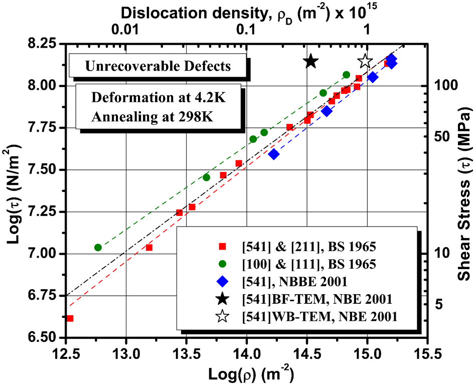
Shear yield stress as function of density of defects that remain in crystals after annealing at room temperature (unrecoverable defects). BS 1965 and NBBE 2001 represent electrical resistivity measurements by Basinski and Saimoto 48 and Niewczas et al. 16 on copper single crystals with orientations marked on figure. NBE 2001 data points represent average dislocation density figures determined from TEM; BF-TEM and WB-TEM represent measurements carried out under strong and weak beam diffracting conditions respectively. 20 Black dashed line has one-half slope in log (τ)–log (ρ) coordinates. Sample data are given in Table 2
Analysis of exponent n and strengthening coefficient αs in constitutive relation τ = αsμ
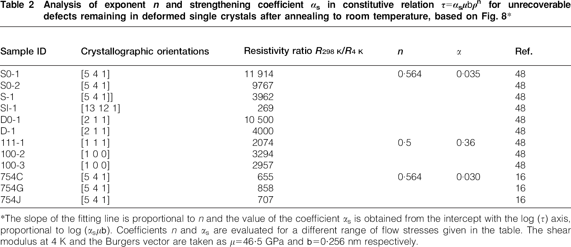
*The slope of the fitting line is proportional to n and the value of the coefficient αs is obtained from the intercept with the log (τ) axis, proportional to log (αsμ
Debris strengthening in single crystals at 4 K
Apart from recoverable defects that make a relatively small contribution to the flow stress (section on ‘Production of vacancies during plastic flow’), plastic deformation at 4 K produces dislocation debris with a spectrum of sizes and strengths that are stable at temperatures higher than room temperature and constitute part of the unrecoverable component of deformation induced defects.16,20,21 They influence the flow stress and the workhardening. 6 Quantitatively, one can expect that the strengthening arising from such debris should resemble elements of the strengthening processes in as irradiated materials. 79 The interaction of dislocations with defects introduced during irradiation occurs through complex processes, which often involve destruction and removal of irradiated defects along the path of moving dislocations. 80 The same might be true for dislocations interacting with debris structure. 6
For the obstacles with the same effective strength μ
 , where τ1 and τ2 are the strengths of first and second set of obstacles with different densities.
82
For obstacles with substantial difference in strength and density, a linear superposition law applies where the total glide resistance is the linear sum of the glide resistance of different kinds of obstacles τ≈τstrong+τweak, where τstrong and τweak are the strengths of weak and strong obstacles contributing to the flow stress.
83
, where τ1 and τ2 are the strengths of first and second set of obstacles with different densities.
82
For obstacles with substantial difference in strength and density, a linear superposition law applies where the total glide resistance is the linear sum of the glide resistance of different kinds of obstacles τ≈τstrong+τweak, where τstrong and τweak are the strengths of weak and strong obstacles contributing to the flow stress.
83
Deformation induced defects, which include point defect clusters, forest dislocations, various sizes SFTs, dipoles and/or loops, exhibit a broad spectrum of strengths. The interactions of dislocations with point defect clusters are expected to be weaker than the interactions with faulted dipoles or larger SFTs. The effective slip resistance that dislocations experience while propagating through this structure is characterised by activation area and activation distance, which can be measured experimentally. 84 These results show that, under common deformation conditions, the activation distance can be traced back to dislocation interactions with various defects present in the microstructure which control the flow process. 85 However, the activation distance at 4 K has been found to be a small fraction of the Burgers vector, indicating that the rate controlling obstacles are characterised by a very narrow energy barrier.85–87 The process has been tentatively attributed to the zero-point energy effects and tunnelling of dislocations through the obstacles85,87, but it is unclear how it relates to the microstructure and processes discussed in the sections on ‘Geometry of crystal deformation and intermittent slip’ and ‘Intermittent flow of dislocations, production of point defects and debris’ and to the SOC.
To estimate the contribution of debris to the plastic flow of single crystals at 4 K, we suppose that only two types of obstacles determine the flow stress: forest dislocations characterised by their glide resistance τforest and debris with glide resistance τdebris. The total glide resistance is thus governed by the linear superposition of strengthening from dislocations and debris τ≈τforest+τdebris. 83 The density of defects stored in the microstructure of <541> single crystals deformed at 4 K and annealed at 298 K was estimated under TEM strong and weak beam diffracting conditions, which permits to differentiate between dislocations and debris (see Table 1 in Ref. 20). These data are reproduced in Fig. 8. The reference flow stress of the single crystal measured after annealing at 298 K, containing dislocations and debris, is τ≈140 MPa; the dislocation densities obtained under strong and weak beam conditions are shown by black and white stars in Fig. 8. 16 The results, although subject to an error about 10–20, indicate that there is a factor of almost 3 difference between dislocation densities determined from strong and weak beam TEM and a factor of almost 5 difference between strong beam TEM and electrical resistivity measurements (Table 1, 20 Fig. 8).
Using the density of dislocations ρ≈3·4×1014 m−2 measured under bright field TEM 20 and the strengthening parameters corresponding to this microstructure n≈0·564 and αs≈0·03 given in Table 2, the flow stress from dislocations is estimated as τ≈56 MPa. The difference between the reference stress and the stress from dislocations stored in the foil is therefore ∼85 MPa, and it is attributed to the contribution of debris to the flow stress. One can expect that the TEM technique underestimates dislocation density in the material, as discussed by Sauzay and Kubin, 77 in which case the figure of 85 MPa would represent an upper limit of debris contribution to the flow stress. To estimate the lower limit of debris contribution to the flow stress, we use density of dislocations determined under higher resolution weak beam TEM, which is capable of resolving part of the fine debris stored in the microstructure (e.g. Fig. 3a), and assume that the difference between the reference (measured) flow stress and the flow stress estimated from the density of dislocations determined under weak beam diffraction conditions arises from debris that have not been detected under weak beam TEM. For the density of dislocations ρ≈9·6×1014 m−2 determined under weak beam TEM, 20 the flow stress is τ≈100 MPa. Thus, the difference between reference flow stress and the estimated flow stress is ∼40 MPa, which represents the lower limit of debris contribution to the flow stress in the single crystal. The average between upper and lower limit of about 60–65 MPa seems to be a reasonable value and indicates that debris may account for 40–50 of the flow stress in <541> single crystals deformed to large strains at 4 K.
It is expected that debris constitute a spectrum of obstacles with different strengths ranging from easily sharable to almost impenetrable obstacles, as observed elsewhere in the case of SFTs interacting with incoming dislocations.88,89 For strong obstacles represented by effective strength ˜μ
 is about 1·8×10−7 m corresponding to the density of debris per unit volume c0 = 1·2×1023 m−3 where
  and
and 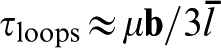 , where in this case
  is the the average spacing of loops intersecting the glide plane. The loop spacing on the glide plane would than be about 6·1×10−8 m, corresponding to the density of loops per unit volume ∼1·0×1024 m−3. Thus, figures 1023 and 1024 m−3 would represent lower and upper density of debris in the structure of <541> single crystals deformed to the end of region A at 4 K. Considering that more debris is expected to be produced at 4 K than at higher temperatures, the results show good agreement with TEM measurements of debris density in single crystals deformed at 78 K.
21
is the the average spacing of loops intersecting the glide plane. The loop spacing on the glide plane would than be about 6·1×10−8 m, corresponding to the density of loops per unit volume ∼1·0×1024 m−3. Thus, figures 1023 and 1024 m−3 would represent lower and upper density of debris in the structure of <541> single crystals deformed to the end of region A at 4 K. Considering that more debris is expected to be produced at 4 K than at higher temperatures, the results show good agreement with TEM measurements of debris density in single crystals deformed at 78 K.
21
Mean free path and mean slip distance
The rate of dislocation accumulation during the athermal region of plastic flow is given in terms of dislocation mean free path
90
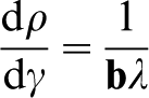
Total dislocation density as function of shear strain for <100> (sample no. 734C) and <541> (sample no. 754F) copper single crystals deformed continuously at 4 K: a range of strains includes deformation of <100> crystals to failure and region A of deformation before twinning in <541> crystals and b region of higher strains revealing differences in behaviour of defect density in <100> and <541> crystals; it is seen that while rate of defect accumulation dρ/dγ is practically unchanged in <10> crystals, a small decrease in dρ/dγ with γ is observed in <541> single crystals
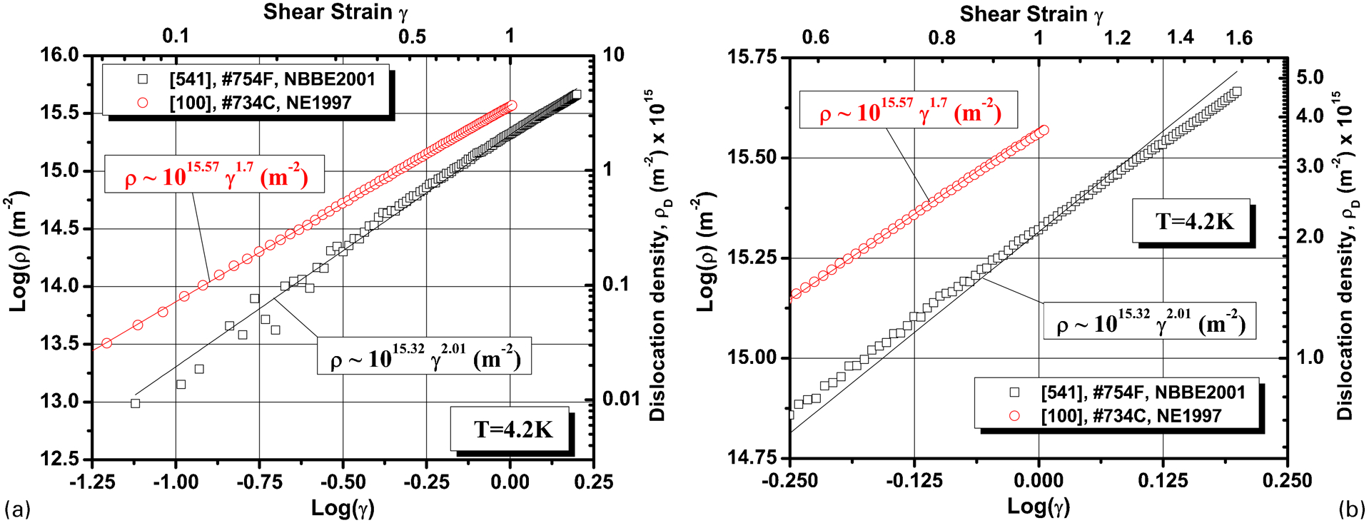
Evolution of dislocation mean free path in <541> and <100> single crystals as function of a shear strain and b shear stress
In this form, λ represents an average dislocation path for mobile dislocations between collisions with unspecified, homogeneously distributed obstacles; it does not differentiate among types of lattice defects that trap dislocations nor does it account for the composite nature of the material containing walls and cells, as seen in Figs. 2 and 3. Figure 10a reveals some differences in the behaviour of λ as a function of shear strain between <541> and <100> single crystals. As expected for <100> crystal, the mean free path decreases rapidly at the beginning of plastic flow and approaches the value of ∼0·5 μm at the point of fracture at the shear strain of ∼1. Somewhat slower development of the microstructure expressed in the lower rate of mean free path decrease is observed for <541> crystal. However, also in this case, the mean free path decreases to the value of ∼0·5 μm, matching reasonably well the size of the cell structure observed by TEM in <541> (Figs. 2b and 3b). The behaviour of λ plotted as a function of shear stress shows that <541> single crystal exhibits a somewhat faster rate of mean free path decrease than the <100> sample, as shown in Fig. 10b.
If the total dislocation density is given by a rule of mixture, ρT = ρwfw+ρc(1−fw), one can attempt to compute the evolution of dislocation density and the dislocation mean free path in the walls and in the cells as a function of strain to explore if any of these parameters correlate with the processes that may influence plastic flow behaviour (e.g. occurrence of stage III, occurrence of twinning, failure point, etc.)
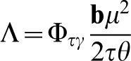
In the kinematic description of the workhardening, the average distance that a dislocation travels between obstacles, termed the mean slip distance Λ, is related to the product of flow stress and the workhardening rate as84,91,92
The quantity τθ needed to calculate Λ is plotted in Fig. 11 for two samples. The curves show the region of linear increase in τθ versus τ, corresponding to stage II of workhardening followed by the deviation from linear behaviour and development of negative curvature, characteristic of stage III. The slope of the linear region represents an athermal component θ0 of the workhardening rate θ. θ0≈207 MPa or μ/225 observed for <100> is almost twice as large as θ0≈110 MPa or μ/423 for the <541> sample, and it extends over a broader range of flow stresses (Fig. 11). The higher stress region where the τθ curve develops a negative slope has been linked to thermally activated dynamic recovery processes understood as being caused by a dislocation collapse and dislocation rearrangements taking place during stage III. 90 Brown interprets this as the exhaustion stage of SOC resulting from the ‘exhaustion of the structures produced by the confined slip in stage II’. Accordingly, the splitting and disintegration of the dipole clumps under the high stress and release of new mobile dislocations increases the amount of strain per increment of stress and is responsible for the decrease in the workhardening rate during the plastic flow. 6
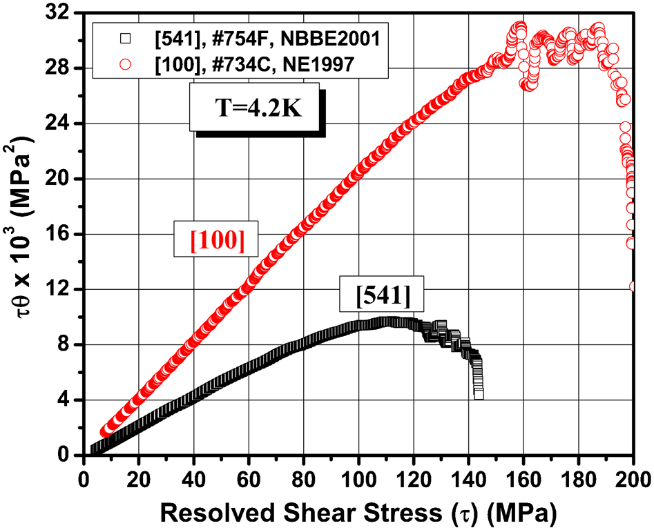
Characteristics of flow stress and workhardening product τθ as function of shear stress for <100> and <541> single crystals, needed to evaluate the mean slip distance Λ
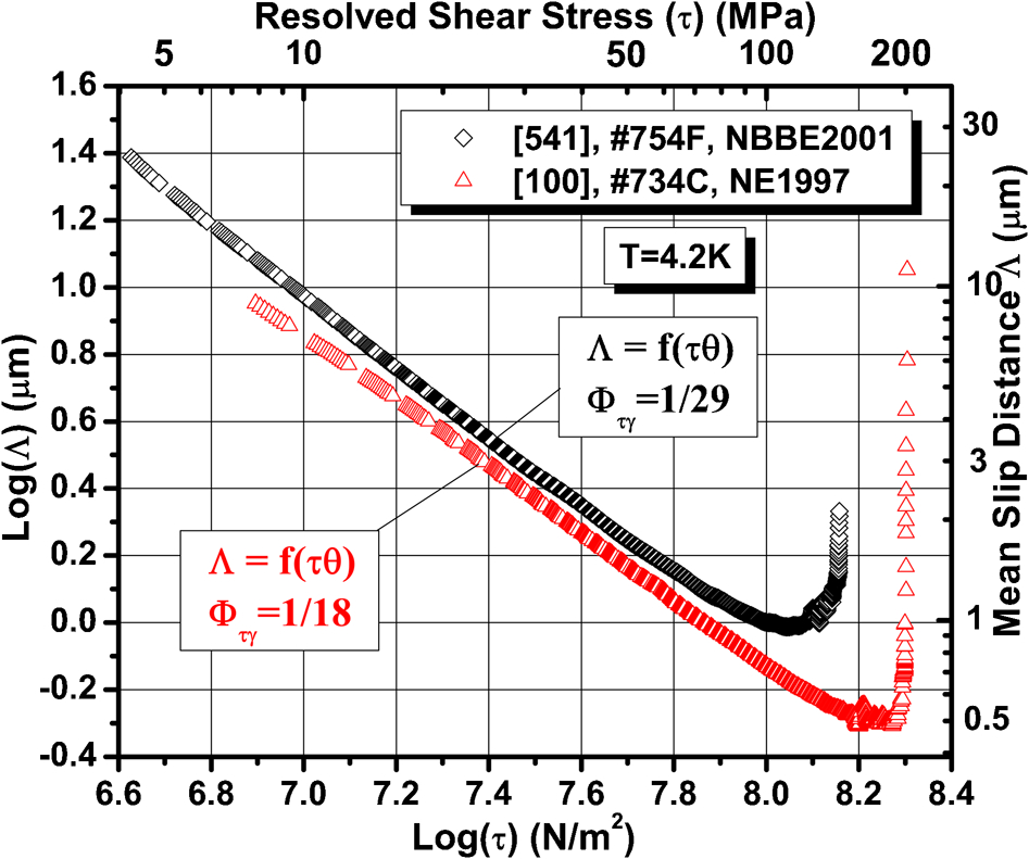
By considering the behaviour of the mean slip distance Λ in relation to the behaviour of the dislocation mean free path λ as a function of flow stress, one can calibrate the workhardening model and use the mean slip distance as a physical parameter representing the length scale of the microstructure that determines the flow stress and workhardening. Figure 12 shows these correlations for <541> (Fig. 12a) and <100> single crystals (Fig. 12b and c). In order to match Λ with λ the value of Φ τγ in the expression for Λ has to be adjusted individually for every crystal orientation. For <541> single crystal, Φ τγ = 1/29 gives good overlap of two curves during stage II of workhardening up to about 70–80 MPa. Beyond 100 MPa, the deviation of the curves is apparent; λ continues to decrease further, whereas Λ, after attaining a minimum value of ∼1 μm, turns up and starts increasing, as seen in Fig. 12a and b. For <100> single crystal, reasonably good correlation of Λ and λ during initial stage of plastic flow up to ∼50 MPa is obtained with Φ τγ = 1/18 (Fig. 12b). In this case, Λ continues to decrease down to a minimum value of Λmin≈0·5 μm, while λ deviates slightly up. It is not clear at the moment what is the reason of such behaviour for <100> single crystal and if it has a physical significance. This has to be explored further. Φ τγ = 1/14 produces better matching of two curves at higher stresses for <100> single crystal (Fig. 12c).
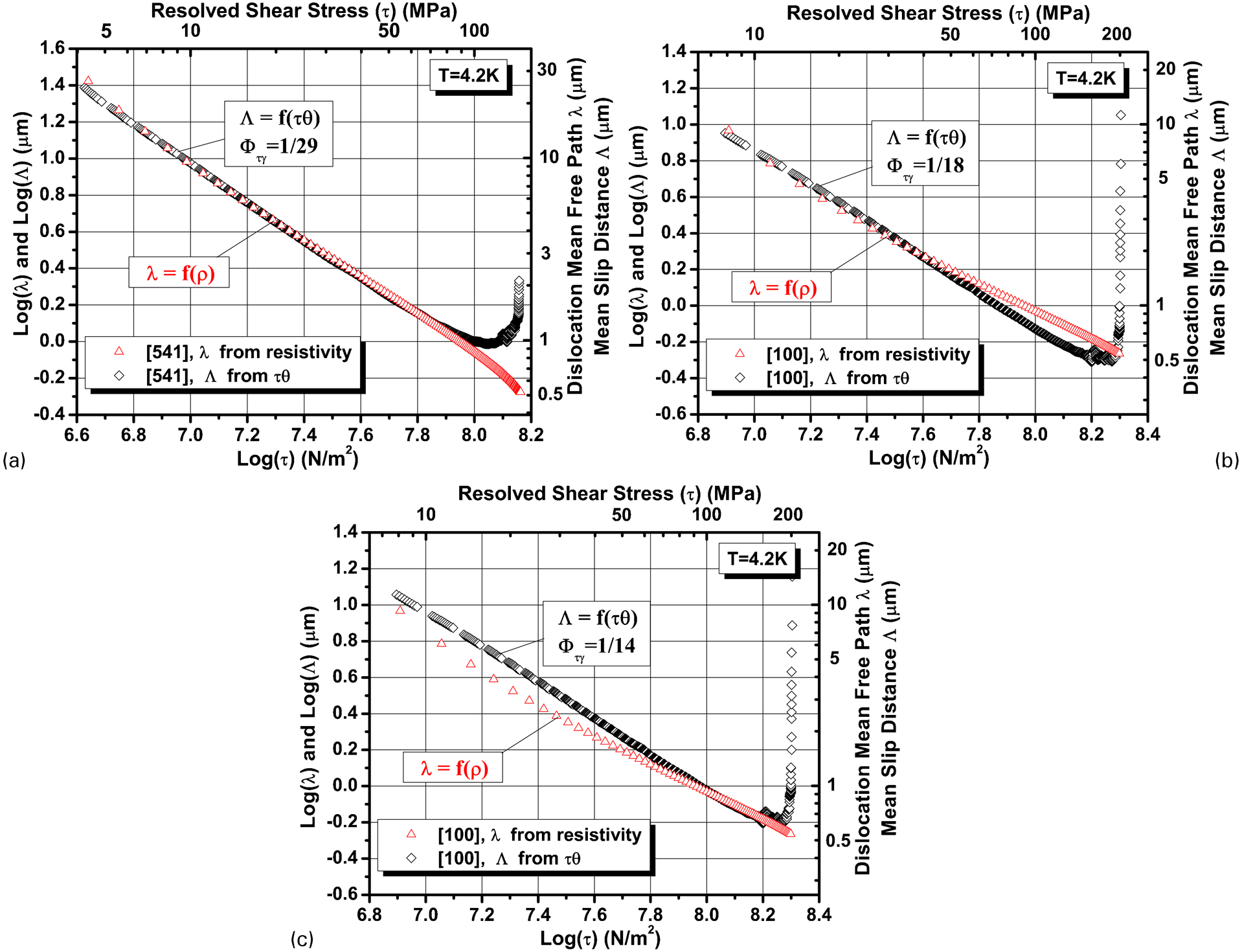
a <541> orientation shows excellent matching of Λ and λ in stage II and deviation in stage III of deformation; b <100> orientation showing excellent matching of Λ and λ in stage II and deviation in stage III, however with opposite trend to a; c matching of Λ and λ at higher stresses in <100> single crystal
The kinematic formalism defines the constant Φ τγ in terms of other constants p, w, r and n characteristic of the workhardening model such that: Φ τγ = pw2/rn. Here, n is the number of successive dislocation loops emitted by the source, w≈1/α is the obstacle strength and p and r are areal and perimeter geometric constants. For circular loops emitted by the source, p≈π/4, r≈π and using α values (0·25 and 0·48) corresponding to <100> and <541> orientation (Table 1), the number of dislocations engaged in the slip event is estimated as 32 and 57 for <100> and <541> single crystals during stage II of workhardening. These figures are within a factor of 2–3 of the figures estimated by Brown, and also within the range between 20 and 1000 assumed by any existing theory of workhardening. 91 This provides independent verification of electrical resistivity data and indicates that the parameter λ can be used as reference to evaluate the microstructural variables that represent the microstructure and determine mechanical response and to derive more robust workhardening models.
The behaviour of Λ as a function of shear stress for two orientations, with Φ τγ coefficients determined in Fig. 12a and b, is shown in Fig. 13. For <100> single crystal Λmin≈0·5 μm matches reasonably well the scale of the microstructure formed at these stress levels. 93 On the other hand Λmin≈1 μm observed in <541> single crystal is a factor of 2 larger than the cell size (Figs. 2b and 3b). Further tuning of Φ τγ constants can produce good overlap of two relationships within stage II, but the difference in Λmin will remain, and the question is whether it is physically significant. In order to answer this question, we refer back to the results discussed in the section on ‘Geometry of crystal deformation and intermittent slip’ in reference to Figs. 1–3 and examine the relationship between Λ, the flow pattern and the features of the microstructure.
The results suggest that the turning point of the mean slip distance in Fig. 12a is associated with the onset of localised shear events occurring at the onset of stage III at 4 K represented by microstructural features visible in Figs. 1 and 2. The value of Λmin≈1 μm represents probably some principal slip transmission distance for the secondary slip systems and primary deformation bands that is longer than a basic wavelength of the microstructure. This will require the operating dislocations to cut through the bands and/or walls and presumably will be associated with increased production of debris and other fine byproducts, as shown in Fig. 3. The softening of the microstructure induced by this kind of relaxation process in <541> single crystals is real because it leads to a small but evident decrease in the rate of defect accumulation dρ/dγ measured independently by electrical resistivity, an indication that the structure is characterised by somewhat lower capacity for defect storage (Fig. 9). This effect is not observed in <100> single crystals (Fig. 9), and we believe that the reason relies on the nature of the intermittent slip linked to the type of microstructure that is produced in these crystals.
The lower Λmin≈0·5 μm observed in <100> orientation in comparison to Λmin≈1 μm in <541> crystals (Fig. 11) stems, in our view, from the range of attributes which differentiate the plastic flow in two orientations, the main reason being that the microstructural instabilities are induced at somewhat higher stresses in <100> crystals. This is associated with the following processes: the geometry of deformation is different in two crystals; <100> represents a stable orientation experiencing only small fluctuations of orientation during plastic flow, which promotes more homogeneous deformation on a microscopic scale. <100> single crystals develop more balanced and well compensated cell-like dislocation microstructure containing many Burgers vectors and of distinct spatial arrangement. The resistance of this microstructure to the interactions with the secondary slip, its stability and storage capacity being higher, is reflected in the higher flow stress and the workhardening rate. At the same stress levels, <100> single crystals store lower density of dislocations than <541> crystals (Figs. 6 and 7); this may help to delay the onset of the relaxation processes occurring in the microstructure when the stored energy is being released. The relaxation occurring in <100> crystals is associated with lower frequency of adiabatic instabilities and smaller stress drops. The shear bands replacing approximately equaxed cell structure are observed at high flow stresses close to the failure, indicating that the relaxation processes encompassing slip transmission on large distances and localised deformation are delayed in comparison to <541> crystals. This affects τθ characteristics and the mean slip distance, which reaches a minimum at a higher flow stress (Fig. 13).
It is interesting to note that the microstructural instabilities accompanying the deformation of <100> single crystals do not produce softening of the microstructure as observed in the behaviour of dρ/dγ, which shows an unchanged rate of defect storage during the stage III deformation where these instabilities are common. This indicates that the strength of the obstacle structure and presumably also types of interactions that dominate the flow stress behaviour are unchanged during the evolution of this microstructure.
The decrease in the macroscopic workhardening rate  accompanying the monotonic behaviour of the rate of accumulation of global defect density dρ/dγ, supports the view that stage III is induced by plastic slip instabilities to reduce long range fluctuations of the local stress and plastic shear strain rate developed during intermittent flow of single crystals.
17
This could produce some of the microstructural inhomogenities observed here (e.g. Fig. 2a). Indeed, the changes in relative dislocation density fluctuations in the transition from stage II to stage III in <100> and <541> copper single crystals deformed at 193 and 300 K have been confirmed independently by X-ray line profile analysis by Szekely and co-workers.
94
accompanying the monotonic behaviour of the rate of accumulation of global defect density dρ/dγ, supports the view that stage III is induced by plastic slip instabilities to reduce long range fluctuations of the local stress and plastic shear strain rate developed during intermittent flow of single crystals.
17
This could produce some of the microstructural inhomogenities observed here (e.g. Fig. 2a). Indeed, the changes in relative dislocation density fluctuations in the transition from stage II to stage III in <100> and <541> copper single crystals deformed at 193 and 300 K have been confirmed independently by X-ray line profile analysis by Szekely and co-workers.
94
Summary
The review of selected experimental work on the relationship between mechanical, electrical and structural properties of single crystals subjected to plastic deformation suggests that the following general conclusions can be drawn:
The macroscopic geometry of a single crystal deformation determines the mechanical properties and plays a critical role in selecting the slip systems and regulating the amount of slip in different slip systems. The change of the dominant operating slip system or the activation of a formally inactive slip system may induce relaxation in the microstructure associated with strain localisation and decrease in the global workhardening rate. Under such circumstances, the secondary slip in addition to its strengthening and stabilising power may act as a destructive element producing soft paths and local disintegration of the primary structures. Typically, this has a signature of slip in alien distributions of dislocations. The resulting effect is governed by the ability to organise various processes across the length scales and involves complex interplay between the amount of slip in glide systems, principal interactions and the Burgers vectors, the properties of the microstructure and its ability to relieve internal stresses and others.
The coupling between the applied stress, the crystallographic orientation of the lattice and the operating slip systems induces fluctuations of the lattice orientation, which translate into fluctuations of the slip on the microscopic level and fluctuations of the dislocation density. Stage III of workhardening in <541> single crystals deformed at 4 K has been shown to be associated with unusual activity of long range slip in the cross-glide plane and localised character of slip in primary and secondary slip systems, presumably activated in response to the internal stresses. This is reflected in the decrease in the workhardening and the increase in the mean slip distance evaluated based on macroscopic workhardening properties of deformed crystals.
The plastic flow of dislocations is associated with the production of a high density of nanoscale defects of various types. The production of the point defects and their role in the plastic flow should be understood better. The results of electrical resistivity measurements indicate that single vacancies are generated at 4 K in small quantities, if any. Vacancy agglomerates that constitute the recoverable portion of deformation induced defects are presumably residuals of other debris refined to the dimensions of point defect clusters. The results suggest that the effect of recoverable debris on the flow stress and workhardening of single crystals at 4 K is small. This should be verified by suitable experimental and modelling studies. The same is true for single interstitials and small interstitial clusters, although results available in the literature seems to agree that interstitial defects are not produced during deformation.
The origin of unrecoverable debris that constitute the nanoscale component of the dislocation microstructure and their effect on the plastic flow should be studied further. Narrow dislocation dipoles have been the subject of various considerations, and we have reasonably good understanding of how they are formed and how they interact with plasticity. However, debris include also various sized SFTs, faulted dipoles, prismatic loops, clusters of vacancies and perhaps clusters of interstitials. They are stored in extremely large densities in areas containing any dislocation arrangements (bundles, tangles, walls, bands and shear bands). It is not clear if they are formed by the collapse of deformation induced point defects, or by conservative processes. Analysis carried out here suggests that debris contribute substantial amount up to 50 of the flow stress at 4 K, and at large deformations, they are produced in densities approaching 1024 m−3.
Analysis of electrical resistivity data suggests that a close to theoretical relationship between the flow stress and the dislocation density is obtained in a broad range of flow stresses when the total defect content representing the weighted mean of the defect densities stored in walls and cells is considered. This confirms various independent analyses carried out in the literature that the flow stress is determined by the average dislocation density under root mean square approximation.6,90 This is presumably also why various mean field theories are capable so accurately to reproduce mechanical properties of plastically deformed systems and there is still much space for other developments.
The dislocation mean free path derived from electrical resistivity data correlates well with the scale of the dislocation free channels and cells developed in <541> and <100> single crystals at the end of stage III. This indicates that the mean free path represents a microstructural length scale that determines the flow stress and can be used to calibrate other physical variables for the purpose of investigating structural processes or developing robust workhardening models. In the present work, the mean free path has been used to calibrate the macroscopic workhardening model and to obtain another microstructural variable, the mean slip distance. This is carried out by a suitable adjustment of a single value parameter, characteristic for the orientation of single crystals. Two microstructural variables, dislocation mean free path and the mean slip distance show good correlation during stage II. The sudden increase in the mean slip distance during stage III is attributed to the microstructural slip instabilities observed by optical and TEM microscopy.
Footnotes
Acknowledgements
I wish to thank editors of Materials Science and Technology and ultimately Professor Brown for their kind invitation to contribute to this discussion. I am grateful to the reviewers for the constructive comments on the manuscript. Financial support of the NSERC Canada is gratefully acknowledged.